

®
LCDP1521
DUAL LINE PROGRAMMABLE TRANSIENT VOLTAGE
A.S.D.™
SUPPRESSOR FOR SLIC PROTECTION
FEATURES
Dual line programmable transient voltage
■
suppressor
Wide negative firing voltage range:
■
= -150 V max.
V
MGL
Low dynamic switching voltages: VFPand V
■
Low gate triggering current: IGT=5mAmax
■
Peak pulse current: IPP= 15 A (10/1000 µs)
■
Holding current: IH= 150 mA min
■
DGL
DESCRIPTION
This device has been especially designed to
protect 2 new high voltage, as well as classical
SLICs, against transient overvoltages.
Positive overvoltages are clamped by 2 diodes.
Negative surges are suppressed by 2 thyristors,
their breakdown voltage being referenced to -V
BAT
through the gate.
This component presents a very low gate
triggering current (I
) in order to reduce the cur-
GT
rent consumption on printed circuit board during
the firing phase.
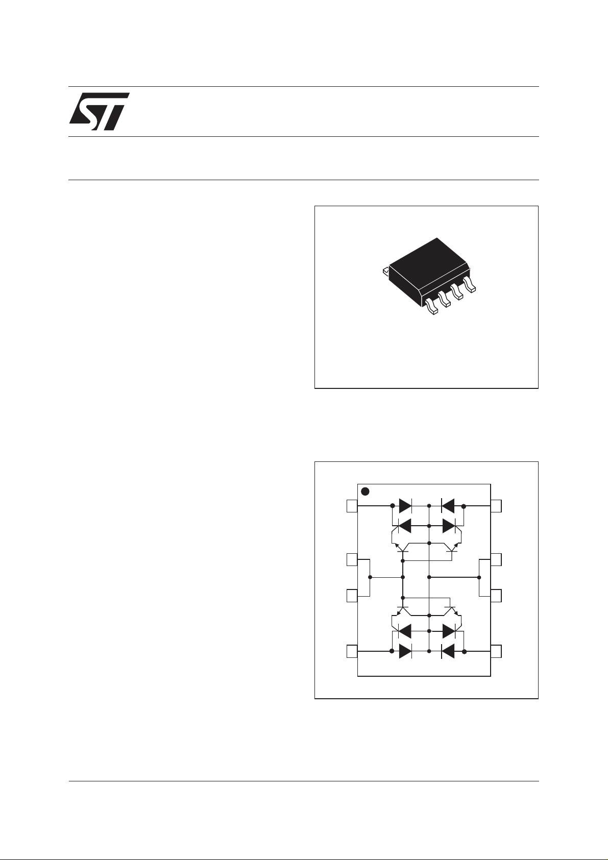
SO-8
FUNCTIONAL DIAGRAM
BENEFITS
Trisils are not subject to ageing and provide a fail
safe mode in short circuit for a better protection.
Trisils are used to help equipment to meet various
standards such as UL1950, IEC950 / CSA C22.2,
UL1459 and FCC part68. Trisils have UL94 V0
resin approved (Trisils are UL497B approved (file:
E136224)).
March 2002 - Ed: 1A
1
TIP 1 RING 1
2
GATE
3
GATE
TIP 2
4
8
7
6
5
GND
GND
RING 2
1/8
LCDP1521
IN COMPLIANCES WITH THE FOLLOWING STANDARDS
STANDARD
GR-1089 Core
First level
GR-1089 Core
Second level
GR-1089 Core
Intra-building
ITU-T-K20/K21
ITU-T-K20
(IEC61000-4-2)
VDE0433
VDE0878
IEC61000-4-5
FCC Part 68, lightning
surge type A
FCC Part 68, lightning
surge type B
Peak Surge
Voltage
(V)
2500
1000
Voltage
Waveform
2/10µs
10/1000µs
Required
peak current
(A)
500
100
Current
Waveform
2/10µs
10/1000µs
Minimum serial
resistor to meet
5000 2/10µs 500 2/10µs 62
1500 2/10µs 100 2/10µs 7
6000
1500
8000
15000
4000
2000
4000
2000
4000
4000
1500
800
10/700µs 150
5/310µs 200
37.5
1/60 ns ESD contact discharge
ESD air discharge
10/700µs 100
5/310µs 120
50
1.2/50µs 100
1/20µs 27
50
10/700µs
1.2/50µs
10/160µs
10/560µs
100
100
200
100
5/310µs
8/20µs
10/160µs
10/560µs
1000 9/720µs 25 5/320µs 0
standard (Ω)
31
57
20
0
0
40
0
120
27
43
32
THERMAL RESISTANCE
Symbol Parameter Value Unit
Rth (j-a)
ELECTRICAL CHARACTERISTICS (T
Symbol Parameter
I
GT
I
H
I
RM
I
RG
V
RM
V
GT
V
F
V
FP
V
DGL
V
GATE
V
RG
C
Junction to ambient
= 25°C)
amb
Gate triggering current
Holding current
Reverse leakage current LINE / GND
Reverse leakage current GATE / LINE
Reverse voltage LINE / GND
Gate triggering voltage
Forward drop voltage LINE / GND
Peak forward voltage LINE / GND
Dynamic switching voltage GATE / LINE
GATE / GND voltage
Reverse voltage GATE / LINE
Capacitance LINE / GND
170 °C/W
I
V
V
RM
R
V
F
I
RM
I
R
I
H
I
PP
V
2/8
LCDP1521
ABSOLUTE RATINGS (T
= 25°C, unless otherwise specified).
amb
Symbol Parameter Value Unit
I
I
TSM
PP
Peak pulse current (see note1)
Non repetitive surge peak on-state
current
10/1000µs
8/20µs
10/560µs
5/310µs
10/160µs
1/20µs
2/10µs
t = 10ms
t=1s
15
60
20
25
30
60
70
5
3.5
(50Hz sinusoidal)
I2t
I
t = 10ms 0.125 A
2
t value for fusing
(50Hz sinusoidal)
I
GSM
Maximum gate current
t = 10ms 2 A
(50Hz sinusoidal)
V
V
MLG
MGL
T
Tj
T
stg
Maximum voltage LINE/GND
Maximum voltage GATE/LINE
Storage temperature range
Maximum junction temperature
L
Maximum lead temperature for soldering during 10s
-40°C < Tamb < +85°C
-40°C < Tamb < +85°C
-150
-150
-55to+150
150
260 °C
A
A
V
°C
2
s
Repetitive peak pulse current
tr: rise time (µs)
tp: pulse duration (µs)
ex: Pulse waveform 10/1000µs
tr = 10µs tp = 1000µs
PARAMETERS RELATED TO THE DIODE LINE / GND (T
amb
%I
100
50
0
= 25°C)
PP
t
t
p
r
t
Symbol Test conditions Max Unit
V
F
V
FP
(note 1)
Note 1:seetest circuit for VFP;RSis the protection resistor located on the line card.
IF=1A
10/700µs
1.2/50µs
2/10µs
1.5kV
1.5kV
2.5kV
R
R
R
S
S
S
= 110Ω
=60Ω
= 245Ω
t = 500µs 2 V
I
PP
I
PP
I
PP
= 10A
= 15A
= 10A
5
10
20
V
3/8

LCDP1521
PARAMETERS RELATED TO THE PROTECTION THYRISTOR (T
= 25°C unless otherwise specified)
amb
Symbol Test conditions Min Max Unit
I
GT
I
H
V
GT
I
RG
V
V
at I
VRG= -150V
V
V
DGL
V
10/700µs
1.2/50µs
2/10µs
Note 2: see functional holding current (IH) test circuit
Note 3: see test circuit for V
The oscillations with a time duration lower than 50ns are not taken into account
PARAMETERS RELATED TO DIODE AND PROTECTION THYRISTOR (T
= -48V
GND / LINE
= -48V (note 2)
GATE
GT
= -150V
RG
= -48V (note 3)
GATE
DGL
1.5kV
1.5kV
2.5kV
R
R
R
S
S
S
= 110Ω
=60Ω
= 245Ω
Tc=25°C
Tc=85°C
I
= 10A
PP
I
= 15A
PP
I
= 10A
PP
0.1 5 mA
150 mA
2.5 V
5
50
5
10
20
= 25°C, unless otherwise
amb
specified)
Symbol Test conditions Typ. Max. Unit
I
RM
C
V
GATE / LINE
V
GATE / LINE
V
R
V
R
= -1V VRM= -150V
= -1V VRM= -150V
= 50V bias, V
= 2V bias, V
= 1V, F = 1MHz
RMS
= 1V, F = 1MHz
RMS
Tc=25°C
Tc=85°C
5
50
20
48
µA
V
µA
pF
4/8

FUNCTIONAL HOLDING CURRENT (IH) TEST CIRCUIT : GO-NO GO TEST
LCDP1521
V
BAT
R
= - 100V
D.U.T
Surge generator
Thisisa GO-NO GOtestwhich allowstoconfirm the holdingcurrent(IH)levelin a functionaltestcircuit.
TEST PROCEDURE :
- Adjust the current level at the I
- Fire the D.U.T. with a surge current : I
value by short circuiting the D.U.T.
H
= 10A, 10/1000µs.
PP
- The D.U.T. will come back to the off-state within a duration of 50ms max.
TEST CIRCUIT FOR VFPAND V
(V is defined in unload condition)P
PARAMETERS
DGL
R4
TIP
L
R2
RING
R3
V
P
C1
R1
C2
GND
Pulse (µs) V
t
r
t
p
p
(V) (µF) (nF) (µH) (Ω)(Ω)(Ω)(Ω) (A) (Ω)
C
1
C
2
LR
1
R
2
R
3
R
4
IPPR
10 700 1500 20 200 0 50 15 25 25 10 110
1.2 50 1500 1 33 0 76 13 25 25 15 60
2 10 2500 10 0 1.1 1.3 0 3 3 10 245
s
5/8

LCDP1521
TECHNICAL INFORMATION
Fig. A1: LCDP1521 concept behavior.
Rs1
L 1
-Vbat
GND
C
IG
Gate
T1
Th1
TIP
D1
ID1
VTip
GND
Rs2
RING
VRing
L 2
Figure A1 shows the classical protection circuit using the LCDP1521 crowbar concept. This topology has been developed to protect the new high voltage SLICs. It allows to program the negative
firing threshold while the positive clamping value is fixed at GND.
When a negative surge occurs on one wire (L1 for example), a current IG flows through the base of the
transistor T1 and then injects a current in the gate of the thyristor Th1. Th1 fires and all the surge current
flows through the ground. After the surge when the current flowing through Th1 becomes less negative
than the holding current I
When a positive surge occurs on one wire (L1 for example), the diode D1 conducts and the surge current
flows through the ground.
The capacitor C is used to speed up the crowbar structure firing during the fast surge edges.
This allows to minimize the dynamical breakover voltage at the SLIC Tip and Ring inputs during fast
strikes. Note that this capacitor is generally present around the SLIC - Vbat pin.
So to be efficient it has to be as close as possible from the LCDP1521 Gate pin and from the reference
ground track (or plan). The optimized value for C is 220nF.
The series resitors Rs1 and Rs2 designed in figure A1 represent the fuse resistors or the PTC which are
mandatory to withstand the power contact or the power induction tests imposed by the various country
standards. Taking into account this fact the actual lightning surge current flowing through the LCDP is
equal to:
I surge = V surge / (Rg + Rs)
, then Th1 switches off.
H
With V surge = peak surge voltage imposed by the standard.
Rg = series resistor of the surge generator
Rs = series resistor of the line card (equivalent to PTC+RonFig. A2)
e.g. For a line card with 60Ω of series resistors which has to be qualified under GR1089 Core 1000V
10/1000µs surge, the actual current through the LCDP1521 is equal to:
I surge = 1000 / (10 + 60) = 14A
The LCDP1521 is particularly optimized for the new telecom applications such as the fiber in the loop,
the WLL, the remote central office. In this case, the operating voltages are smaller than in the classical
system. This makes the high voltage SLICs particularly suitable. The schematics of figure A2 gives the
most frequent topology used for these applications.
6/8

Fig. A2: Protection of high voltage SLICs.
LCDP1521
-Vbat
PTC or Fuse
Line 1
PTC or Fuse
PTC or Fuse
Line 2
PTC or Fuse
Fig. 1: Surge peak current versus overload dura-
tion.
R
LCDPxxxx
TIP
SLIC 1
Ring relay 1
R
RING
R
SLIC 2
Ring relay 2
R
Fig. 2: Relative variation of holding current versus
junction temperature
ITSM(A)
7
6
5
4
3
2
1
0
0.01 0.10 1.00 10.00 100.00 1000.00
t(s)
F=50Hz
Tj initial=25°C
ORDER CODE
LCDP 15 2 1 RL
LINE CARD
DUAL PROTECTION
I = 150 mA
H
IH (Tj ) / IH (Tj=25° C )
1.3
1.2
1.1
1
0.9
0.8
0.7
-40-30-20-100 102030405060708090
Tj ( °C )
PACKAGE
1 : SO-8
VERSION
RL :Tape & Reel
:Tube
7/8

LCDP1521
PACKAGE MECHANICAL DATA
SO-8 (Plastic)
L
A
a2
b
8
1
e
e3
D
M
5
4
S
F
DIMENSIONS
REF.
Millimetres Inches
Min. Typ. Max. Min. Typ. Max.
A 1.75 0.069
c1
C
a3
a
1
E
b
a1 0.1 0.25 0.004 0.010
a2 1.65 0.065
a3 0.65 0.85 0.025 0.033
1
b 0.35 0.48 0.014 0.019
b1 0.19 0.25 0.007 0.010
C 0.25 0.50 0.50 0.010 0.020
c1 45° (typ)
D 4.8 5.0 0.189 0.197
E 5.8 6.2 0.228 0.244
e 1.27 0.050
e3 3.81 0.150
F 3.8 4.0 0.15 0.157
L 0.4 1.27 0.016 0.050
M 0.6 0.024
S 8° (max)
Order code Marking Package Weight Base qty Delivery mode
LCDP1521 CDP152 SO-8 0.08 g 100 Tube
LCDP1521RL CDP152 SO-8 0.08 g 2500 Tape& Reel
Informationfurnished is believed tobe accurate and reliable.However,STMicroelectronics assumes noresponsibilityfor the consequencesof
useof such informationnorfor any infringementof patents or otherrights of thirdpartieswhich may resultfromits use. Nolicense is granted by
implication or otherwise under any patent or patent rights of STMicroelectronics. Specifications mentioned in this publication are subject to
change without notice. This publication supersedes and replaces all information previously supplied.
STMicroelectronics products are not authorized for use as critical components in life support devices or systems without express written
approval of STMicroelectronics.
The ST logo is a registered trademark of STMicroelectronics
© 2002 STMicroelectronics - Printed in Italy - All rights reserved.
STMicroelectronics GROUP OF COMPANIES
Australia - Brazil - Canada - China - Finland - France - Germany
Hong Kong - India - Israel - Italy - Japan - Malaysia - Malta - Morocco - Singapore
Spain - Sweden - Switzerland - United Kingdom - United States.
http://www.st.com
8/8
 Loading...