

LCDP1511D
ApplicationSpecific Discretes
A.S.D.
TM
FEATURES
Duallineprogrammabletransientsuppressor
Widenegative firingvoltagerange: V
Lowdynamicswitching voltages: V
FP
Lowgatetriggeringcurrent : IGT=5mAmax
Peakpulse current: I
Holdingcurrent: I
= 15 A (10/1000µs)
PP
>150mA
H
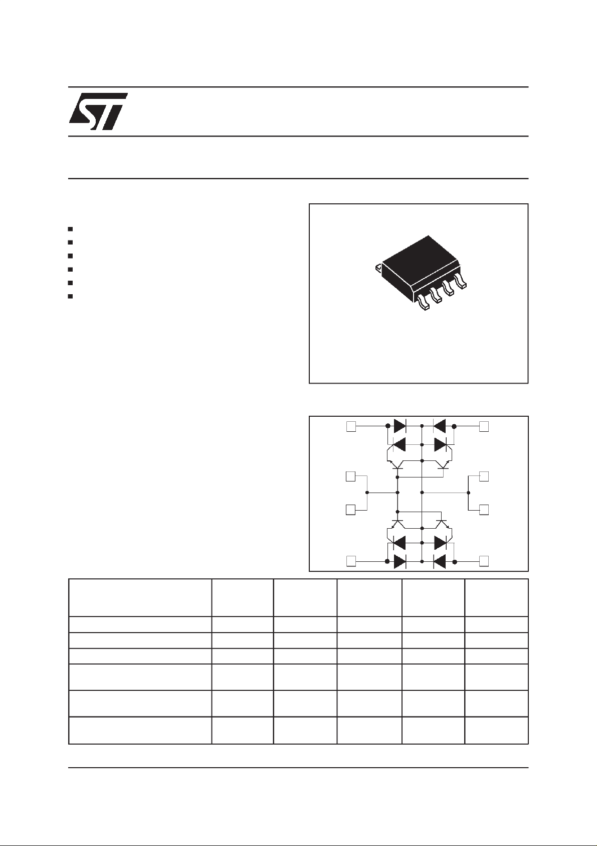
DESCRIPTION
TheLCDP1511Disaduallineprotectorwhichprotects subscriber line interface circuits (SLIC)
againsttransientovervoltages.
Positiveovervoltagesareclamped with diodes towards GND, while negative overvoltages are suppressed by thyristors connected to GND. The
breakdownvoltage of the thyristorsis determined
by the voltageapplied to the gate, generally -V
VOLTAGE SUPPRESSORFOR SLIC PROTECTION
= -80V
MGL
and V
DGL
bat
DUAL LINE PROGRAMMABLE TRANSIENT
SO8
FUNCTIONAL DIAGRAM
.
TIP 1 RING 181
COMPLIESWITH THE
FOLLOWINGSTANDARDS:
ITU-T K20
VDE0433
VDE0878
IEC1000-4-5
FCC Part 68
BELLCORE NWT-001089-CORE
September 1999 - Ed:2A
GATE
2
GATE
3
TIP 2 RING 2
PeakSurge
Voltage
(V)
Voltage
Waveform
(µs)
Current
Waveform
(µs)
Admissible
Ipp
(A)
1000 10/700 5/310 25 2000 10/700 5/310 25 40
1500 1.2/50 1/20 40 -
level 2
level 2
1500
800
2500
1000
10/700
1.2/50
10/160
10/560
2/10
10/1000
5/310
8/20
10/160
10/560
2/10
10/1000
25
25
30
20
70
15
GND
7
GND
6
54
Necessary
Resistor
(Ω)
-
-
-
5
25
45
1/6
LCDP1511D
ABSOLUTEMAXIMUM RATINGS(T
amb
=25°C).
Symbol Parameter Value Unit
I
PP
I
FSM
V
MLG
V
MGL
T
stg
T
L
Note 1: Pulse waveform
Note 2 :
Maximum current flowing throughthe 4 wires together.
Peakpulse current(see note1)
Non repetitive surgepeak on-state current
(see note2)
Maximum voltage LINE/GND
Maximum voltage GATE/LINE
Storage temperature range
Leadtemperaturefor solderingduring 10s
10/ 1000 µstr=10µs tp= 1000
5 / 310 µstr=5µs tp= 310 µs
2/10µstr=2µstp=10µs
µs
100
%I
PP
10/1000µs
5/310µs
2/10µs
tp= 10ms
t
=1s
p
15
25
70
5
3.5
80
80
- 55 to + 150 °C
260 °C
50
0
t
rp
t
A
A
V
t
THERMALRESISTANCE
Symbol Parameter Value Unit
Rth (j-a)
ELECTRICALCHARACTERISTICS(T
Junction to ambient
amb
170
=25°C)
Symbol Parameter
Gate triggering current
Holding current
Reverse leakage current LINE / GND
Reverse leakage current GATE / LINE
Reverse voltage LINE / GND
Gate triggering voltage
Forward drop voltage LINE / GND
F
Peak forward voltage
Dynamic switching voltage GATE / LINE
GATE / GND voltage
Reverse voltage GATE / LINE
Capacitance LINE / GND
VDGL
VRMVR
VF
IRM
IR
I
I
H
PP
V
V
V
V
V
V
I
GT
I
H
I
RM
I
RG
RM
GT
V
FP
DGL
GATE
RG
C
°
C/W
2/6

LCDP1511D
PARAMETERSRELATED TOTHE DIODE LINE / GND(T
amb
=25°C)
Symbol Testconditions Max Unit
V
F
V
FP
(note1)
note1 : see test circuit for VFP,RPisthe protection resistor located on the linecard
Square pulse : tp=500µsIF=1A
10/700µs
1.2/50µs
2/10µs
1kV
1.5kV
2.5kV
RP=60Ω
R
=60Ω
P
= 245
R
P
I
PP
I
PP
Ω
I
PP
PARAMETERSRELATED TOTHE PROTECTIONTHYRISTOR(T
= 10A
= 15A
= 10A
amb
=25°C)
2V
5
10
20
Symbol Testconditions Min Max Unit
V
I
GT
I
H
V
GT
I
RG
V
DGL
GND / LINE
V
GATE
at I
VRG= -75V
V
GATE
10/700µs
1.2/50µs
2/10µs
note2 : see functional holding current test circuit
note3 : See testcircuit for V
The oscillations with a timeduration lower than 50ns are not takeninto account
PARAMETERSRELATEDTO LINE/ GND
= -48V
=-48V (see note 2)
GT
=-48V (see note 3)
1kV
1.5kV
2.5kV
DGL
R
R
R
P
P
P
=60
=60
=245
(T
Ω
Ω
Ω
amb
I
= 10A
PP
I
= 15A
PP
I
= 10A
PP
=25°C)
5mA
150 mA
2.5 V
5 µA
7
15
20
V
V
Symbol Test conditions Max Unit
I
Fig.1:
V
RM
C
GATE/ LINE
VR= -3V F = 1MHz
V
= -48V F = 1MHz
R
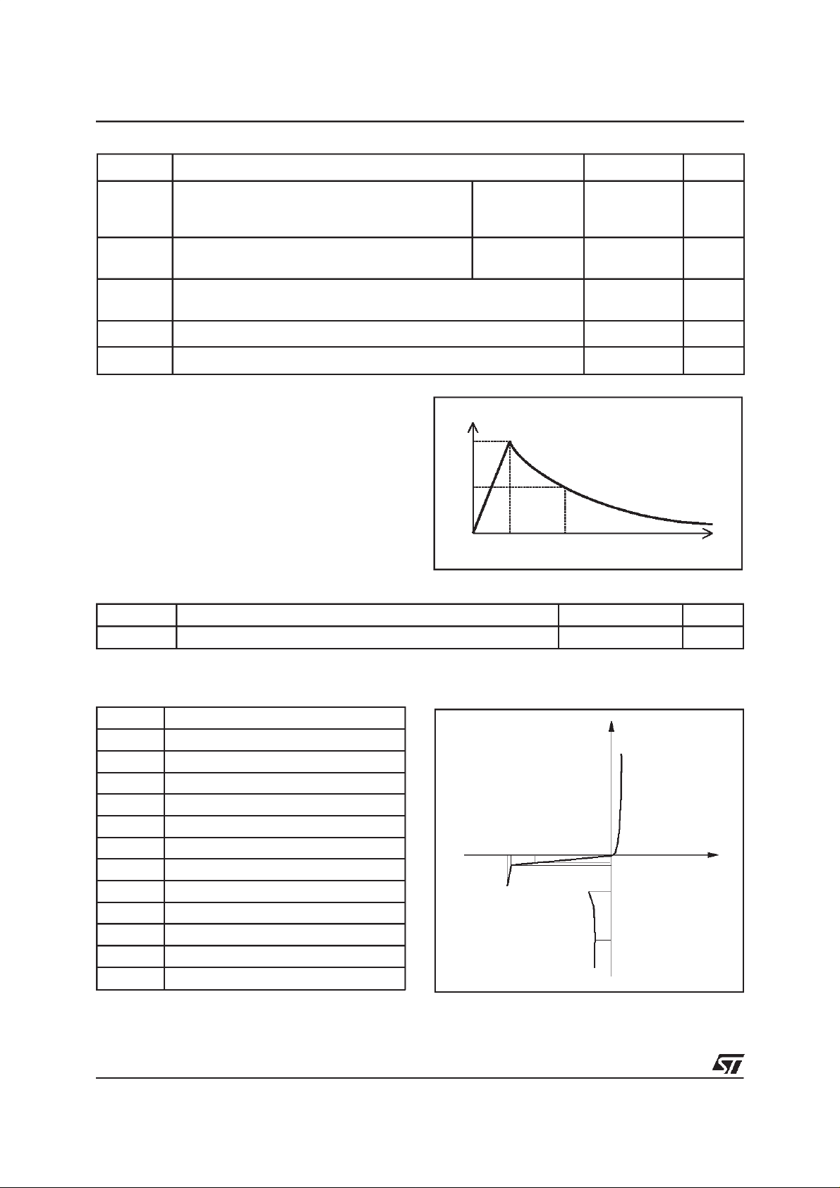
Surgepeakcurrentversusoverloadduration.
= -1V VRM= -75V
Fig. 2:
5 µA
200
100
Relativevariation of holding current versus
junctiontemperature.
ITSM(A)
7
6
5
4
3
2
1
0
0.01 0.10 1.00 10.00 100.00 1000.00
t(s)
F=50Hz
Tj initial=25°C
IH[Tj] / IH[Tj=25°C]
2.0
1.8
1.6
1.4
1.2
1.0
0.8
0.6
0.4
0.2
0.0
-40 -20 0 20 40 60 80 100 120
Tj(°C)
pF
3/6

LCDP1511D
FUNCTIONALHOLDING CURRENT (IH) TEST CIRCUIT : GO-NOGO TEST
R
-V
P
V
BAT
=
-48V
D.U.T.
Thisis aGO-NOGO testwhichallowsto confirmthe holdingcurrent(I
TESTPROCEDURE:
- Adjustthe current levelat theI
- FiretheD.U.T. with a surgecurrent : I
valueby short circuitingthe D.U.T.
H
=15A, 10/1000µs.
PP
- The D.U.T.will comeback to theoff-statewithina durationof 50msmax.
TESTCIRCUITFOR V
(V is defined in unload condition)
P
FP
ANDV
PARAMETERS
DGL
L
R
2
Surge generator
)levelin afunctionaltestcircuit.
H
R
4
TIP
RING
R
3
V
CC
P
1
R
1
2
GND
Pulse(µs) V
t
r
t
p
p
(V) (µF) (nF) (µH) (Ω)(
10 700 1000 20 200 0 50 15 25 25 10 60
1.2 50 1500 1 33 0 76 13 25 25 15 60
2 10 2500 10 0 1.1 1.3 0 3 3 10 245
4/6
C
1
C
2
LR
1
R
2
Ω
)(
R
3
Ω
)(
R
4
Ω
IPPR
) (A) (Ω)
p

APPLICATIONCIRCUIT: PABX line protection
LCDP1511D
Line 1
Line 2
PTC or Fuse
PTC or Fuse
PTC or Fuse
PTC or Fuse
Ring relay
protection
Ring relay
protection
Ring
relay
1
Ring
relay
2
LCDP1511D
P
R
R
RPP
P
R
R
R
R
P
-Vbat
SLIC
-Vbat
SLIC
APPLICATIONCIRCUIT: Line Cardprotection
PTC or Fuse
Line 1
PTC or Fuse
PTC or Fuse
Line 2
PTC or Fuse
CLP30-200B1
CLP30-200B1
Ring
relay
1
Ring
relay
LCDP1511D
-Vbat
RP
SLIC
RP
-Vbat
RP
2
P
R
SLIC
5/6

LCDP1511D
PACKAGEMECHANICAL DATA
SO8(Plastic)
L
A
a2
b
8
1
e
e3
D
M
5
4
S
F
DIMENSIONS
REF.
Millimetres Inches
Min. Typ. Max. Min. Typ. Max.
A 1.75 0.069
a1 0.1 0.25 0.004 0.010
c1
C
a3
b
a
1
E
1
a2 1.65 0.065
a3 0.65 0.85 0.025 0.033
b 0.35 0.48 0.014 0.019
b1 0.19 0.25 0.007 0.010
C 0.25 0.50 0.50 0.010 0.020
c1 45°(typ)
D 4.8 5.0 0.189 0.197
E 5.8 6.2 0.228 0.244
e 1.27 0.050
e3 3.81 0.150
F 3.8 4.0 0.15 0.157
L 0.4 1.27 0.016 0.050
M 0.6 0.024
S8°(max)
Ordrecode Marking Package Weight Base qty Deliverymode
LCDP1511D LCDP15 SO8 0.077 g 100 Tube
LCDP1511DRL LCDP15 SO8 0.077 g 2500 Tape& reel
Informationfurnished is believed to be accurate and reliable. However, STMicroelectronics assumes no responsibility for theconsequences of
use of such informationnor for any infringement of patentsor other rightsof third parties which may result from its use. No license is granted by
implication orotherwise under any patent or patent rights of STMicroelectronics. Specifications mentioned in this publicationare subject to
change without notice. This publication supersedes and replaces all information previouslysupplied.
STMicroelectronicsproducts are not authorized for use ascritical components in lifesupport devices or systems without express written approval of STMicroelectronics.
The ST logo is a registeredtrademark ofSTMicroelectronics
1999 STMicroelectronics - Printed inItaly -All rights reserved.
STMicroelectronics GROUP OF COMPANIES
Australia - Brazil - China - Finland - France - Germany -Hong Kong - India- Italy - Japan - Malaysia
Malta - Morocco - Singapore - Spain - Sweden - Switzerland - United Kingdom - U.S.A.
http://www.st.com
6/6
 Loading...