

SGS Thomson Microelectronics L9997ND Datasheet
HALFBRIDGE OUTPUTS WITH TYPICAL
R
= 0.7Ω
ON
OUTPUTCURRENT CAPABILITY±1.2A
OPERATING SUPPLY VOLTAGE RANGE 7V
TO 16.5V
SUPPLY OVERVOLTAGE PROTECTION
FUNCTIONFOR V
UP TO 40V
VS
VERY LOW QUIESCENT CURRENT IN
STANDBYMODE < 1µA
CMOS COMPATIBLE INPUTS WITH HYSTERESIS
OUTPUTSHORT-CIRCUIT PROTECTION
THERMALSHUTDOWN
REAL TIME DIAGNOSTIC: THERMAL OVER-
LOAD, OVERVOLTAGE
L9997ND
DUAL HALF BRIDGE DRIVER
MULTIPOWER BCD TECHNOLOGY
SO20 (12+4+4)
ORDERING NUMBERS:
L9997ND
L9997ND013TR
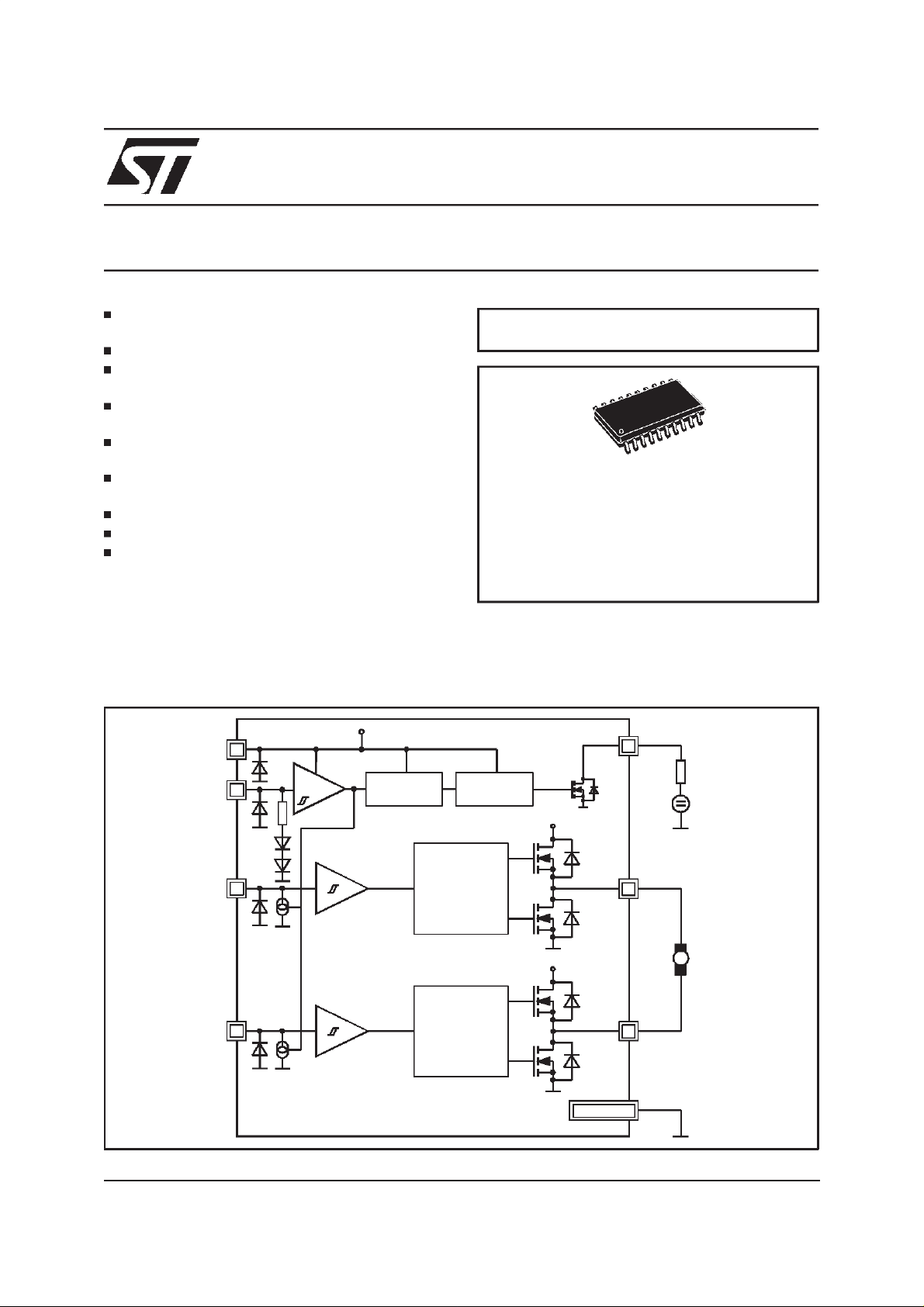
DESCRIPTION
The L9997ND is a monolithic integrated driver, in
BCD technology intended to drive various loads,
BLOCK DIAGRAM
VS VS
1
EN
IN1
IN2
10
12
9
ENABLE
REFERENCE
BIAS
including DC motors. The circuit is optimized for
automotiveelectronicsenviromental conditions.
DIAG
11
PROTECTION
FUNCTIONS
DRIVER 1
DRIVER 2
VS
OUT1
19
VS
OUT2
2
5V
M
April 1999
GND
4...7,1 4...17
1/9
L9997ND
ABSOLUTE MAXIMUM RATINGS
Symbol Parameter Value Unit
V
V
V
V
I
VSDC
VSP
I
OUT
IN1,2
V
EN
DIAG
I
OUT
DIAG
DC Supply Voltage -0.3 to 26 V
Supply VoltagePulse (T < 400ms) 40 V
DC Output Current ±1.8 A
DC Input Voltage -0.3 to 7 V
Enable Input Voltage -0.3 to 7 V
DC Output Voltage -0.3 to 7 V
DC Output Short-circuit Current -0.3V < V
OUT<VS
+ 0.3V internally limited
DC Sink Current -0.3V< VDG< 7V internally limited
PIN CONNECTION
(Topview)
V
S
OUT2
N.C.
GND
GND
GND
GND
N.C.
IN2 IN1
EN DIAG
2
3
4
5
6
7
8
9
10
D95AT166
20
19
18
17
16
15
14
13
12
11
N.C.1
OUT1
N.C.
GND
GND
GND
GND
N.C.
PIN FUNCTIONS
N. Name Function
1 VS Supply Voltage
2 OUT2 Channel 2: Push-Pull power output with intrinsic body diode
3, 8, 13,
18,20
4to7,
14 to 17
9 IN2 Input 2: Schmitt Trigger input with hysteresis(non-inverting signalcontrol)
10 EN Enable: LOW or not connected on thisinput switchesthe device into standby mode andthe
11 DIAG Diagnostic: Open Drain Output thatswitches LOW if overvoltage or overtemperature is
12 IN1 Input 1: Schmitt Trigger input with hysteresis(non-inverting signalcontrol)
NC NC: Not Connected
GND Ground: signal - and power - ground, heat sink
outputs into tristate
detected
THERMAL DATA
Symbol Parameter Value Unit
T
jTS
T
jTSH
R
th j-amb
R
th j-pins
(1) With6cm2on board heatsink area.
2/9
Thermal Shut-down Junction Temperature 165 °C
Thermal Shut-down Threshold Hysteresis 25 K
Thermal Resistance Junction-Ambient
(1)
50 K/W
Thermal Resistance Junction-Pins 15 K/W
L9997ND
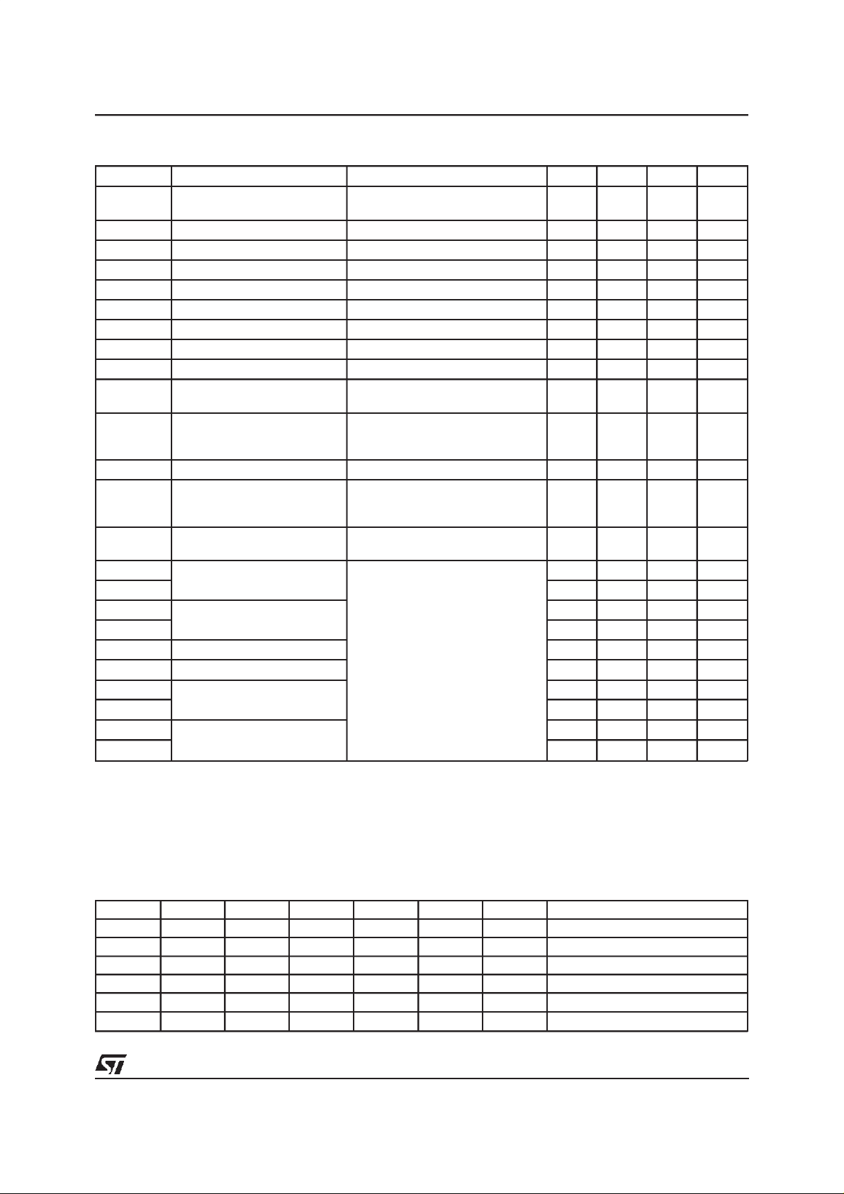
ELECTRICALCHARACTERISTICS (7V < VS< 16.5V;-40°C< TJ< 150°C;unlessotherwisespecified.)
Symbol Parameter Test Condition Min. Typ. Max. Unit
I
VS_SB
I
VS
V
ENL
V
ENH
V
ENthh
I
EN
V
IN1,2L
V
IN1,2H
V
IN1,2thh
I
IN1,2
R
ON OUT1,2
|I
OUT1,2
V
DIAG
V
VSOVth
t
ONLH
t
ONHL
t
OFFHL
t
OFFLH
t
dHL
t
dLH
t
rHS
t
rLS
t
fHS
t
fLS
* Tested at 125°C and guaranteedby correlation
Quiescent Currentin Standby
Mode
Supply Current EN = HIGH, I
VEN< 0.3V;VVS<16.5V;Tj< 85°(*)
V
=0; VVS= 14.5V; Tj =25°C
EN
=0 2 6 mA
OUT1,2
<1
<1
90
10
µA
µA
Low Enable Voltage 1.5 V
High Enable Voltage 3.5 6 V
Enable Threshold Hysteresis 1 V
Enable Input Current VEN= 5V 85 250 µA
Low Input Voltage 1.5 V
High Input Voltage 3.5 V
Input Threshold Hysteresis 1 V
Input Bias Current VIN=0
V
= 5V, EN = HIGH
IN
ON-Resistance to Supply or
GND
I
= ±0.8A; VVS= 7V; Tj= 125°C
OUT
I
= ±0.8A;VVS=12V;Tj= 125°C
OUT
I
= ±0.8A; VVS= 12V; Tj=25°C
OUT
-3
2
0
10
1.2
1.1
1
50
2.8
2.25
µA
µA
0.7
| Output CurrentLimitation 1.2 1.6 2.2 A
Diagnostic OutputDrop I
= 0.5mA, EN = HIGH
DIAG
0.6 V
Overvoltage orThermal Shutdown
Supply Overvoltage
17 19 21 V
Threshold
Turn on Delay Time See Fig. 2; VVS= 13.5V
Measured with 93Ωload
50 150 µs
30 150 µs
Turn off Delay Time 10 100
220µs
Rising Delay Time 115 250
Falling Delay Time 115 250 µs
Rise Time 30 100
60 150 µs
Fall Time 25 100
50 150 µs
Ω
Ω
Ω
s
µ
s
µ
s
µ
s
µ
FUNCTIONAL DESCRIPTION
The L9997ND is a motor driver two half-bridge
outputs, intended for driving dc motorsin automotive systems. The basic function of the device is
shownin the Table1.
Table 1. Table function.
Status EN IN1 IN2 OUT1 OUT2 DIAG NOTE
1 L X X Tristate Tristate OFF Standby Mode
2 H H H SRC SRC OFF Recommended for braking
3 H H L SRC SNK OFF
4 H L H SNK SRC OFF
5 H L L SNK SNK OFF
6 H X X Tristate Tristate ON Overvoltage or Overtemperature
3/9
 Loading...