

■
ONE FULL BRIDGE FOR 6A LOAD (ron= 150mΩ)
■ THREE HALF BRIDGES FOR 1.6 A LOAD
(r
= 800mΩ)
on
■ ONE HIGHSIDE DRIVER FOR 6A LOAD
(r
= 100mΩ)
on
■ VERY LOW CURRENT CONSUMPTION IN
STANDBY MODE (I
■ SERIAL PERIPHERAL INTERFACE (SPI) TO
< 6µA, typ. Tj ≤ 85°C)
S
MICROCONTROLLER
■
ALL OUTPUTS SHORT CIRCUIT PROTECTED
■ CURRENT MONITOR OUTPUT FOR FULL
BRIDGE AND HIGHSIDE DRIVER
■ ALL OUTPUTS OVER TEMPERATURE
PROTECTED
■
OPEN LOAD DIAGNOSTIC FOR ALL OUTPUTS
■
OVERLOAD DIAGNOSTIC FOR ALL OUTPUTS
L9949
DOOR ACTUATOR DRIVER
MULTIPOWER BCD60III TECHNOLOGY
PowerSO20
ORDERING NUMBER: L9949
FULL BRIDGE FOR DOOR LATCH OR
MIRROR RETRACT, HALF BRIDGES FOR
MIRROR AXIS CONTROL AND HIGH-SIDE
DRIVER FOR MIRROR DEFROSTER
APPLICATIONS
■ FOR AUTOMOTIVE APPLICATI ONS, E.G.
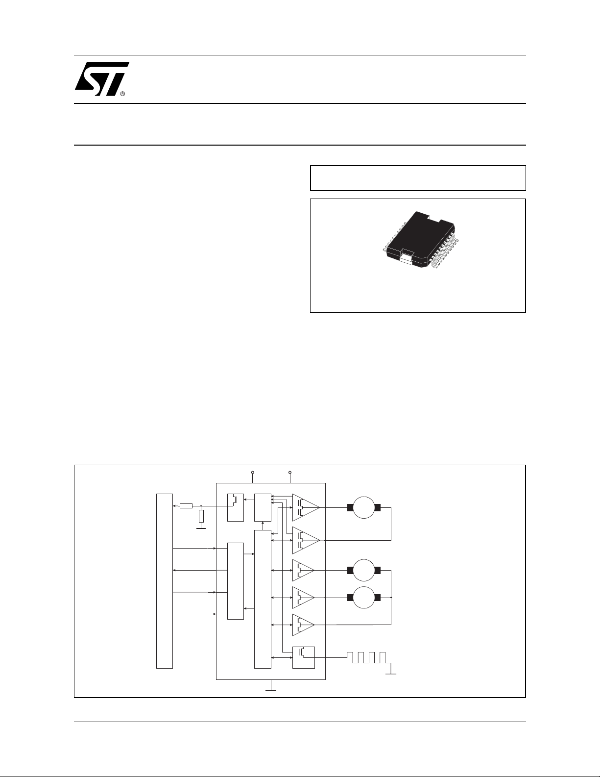
BLOCK DIAGRAM
V
CC
CM
MUX
DI
DO
µC
CLK
CSN
SPI
Driver Interface & Diagnostic
DESCRIPTION
The L9949 is a microprocessor control led power interface for automotive applications. It is realized in
multipower BCD60III technology. Up to three D C mo-
V (battery)
S
OUT1
Full bridge
OUT2
OUT3
Half bridge
OUT4
Half bridge
OUT5
OUT6
Highside driver
M
M
M
e.g. for mirror retract
or door latch
e.g. for mirror
axis control
e.g. for mirror
defroster
September 2002
Ground
1/20

L9949
DESCRIPTION
(continued)
tors and one grounded resistive load can be driven with its three half bridges, one full bridge and one highside
driver power outputs. The integrated standard serial peripheral interface (SPI) controls all operation modes (forward, reverse, brake and high impedance). All diagnostic informations are available via the SPI.
Dual Power Supply: VS and V
CC
The power supply voltage VS supplies the ful l bridge, the half bridges and the highside driver. An internal
charge-pump are used to drive the highside switches. The logic supply voltage V
(stabilized 5V) is used for
CC
the logic part and the SPI of the device. Due to the independent logic supply voltage the control and status information will not be lost, if there are temporary spikes or glitches on the power supply voltage. In case of poweron (V
power-on-reset (POR). If the voltage V
increases from undervoltage t o V
CC
VCC OFF
decreases under the minimum threshold (V
CC
= 4.2V) the ci rcuit i s ini tialized by an internall y generated
VCC ON
= 3.4V), the out-
puts are switched to tristate (high impedance) and the status registers are cleared.
Standby-Mode
The standby mode of the L9949 is activated by setting the bits 12 and 13 of the Input Data Register to zero. All
latched data will be cleared and the inputs and out puts are switc hed to high impedance. In t he st andby mode
the current at V
(VCC) is less than typ. 6µA (40µA) for CSN = high (DO in tristate). By switching the VCC voltage
S
a very low quiescent current can be achieved. If one of the bits 12 and 13 are set to high, the device will be
switched to active mode.
Inductive Loads
Each half bridge is built by internally connected highside and a lowside power DMOS transistor. Due to the builtin reverse diodes of the output transistors inductive loads can be driven at the outputs OUT1 to OUT5 without
external free-wheeling diodes. The highside driver OUT6 is intended to drive resistive loads only hence only a
limited energie (E<1mJ ) can be dissipated by the i nt ernal ESD-diode in f reewheeli ng conditi on. For i nduct ive
loads (L>100
µ
H) an external free-wheeling diode connected to GND and OUT6 is needed.
Diagnostic Functions
All diagnostic functions (over /open load, power supply over-/undervoltage, temperature warning and thermal
shutdown) are internally filtered and the condition has to be valid for at least 10µs (0.5ms, respectively) before
the corresponding status bit in the status registers will be set. The filters are used to improve the noise immunity
of the device. The open load and temperature warning function are intended for informati on purpose and will
not change the state of the output drivers. In contrast, the overload and thermal shutdown condition will disable
the corresponding driver (overload) or all dr ivers ( t hermal shut down), respectiv ely. The micr ocontroller has to
clear the status bits to reactivate the corresponding drivers. This is to avoid an uncontrolled switching behaviour
of the device which may result in a heavy noise on the GND and V
to GND o r V
).
S
lines in case of an fault condition (e.g. short
S
Overvoltage and Undervoltage Detection
If the power supply voltage VS rises above the overvoltage threshold V
SOV OFF
(max. 22V), the outputs OUT1
to OUT6 are switched to high impedance state to protect the load. If the supply voltage recovers to normal operating voltage, the device will return to the programmed state (lockout bit 14 = 0). When the voltage V
below the undervoltage threshold V
SUV OFF
(min. 6V), the output stages are switc hed to high impedance to
drops
S
avoid the operation of the power devices without sufficient gate driving voltage (increased power dissipation). If
the supply voltage V
and the internal charge-pump recovers to normal operating voltage the syste m returns to
S
the programmed state (lockout bit 14 = 0). If the lockout bit 14 is set, the automatic turn-on of the drivers is deactivated. The microcontroller needs to clear the status bits to reactivate the drivers.
2/20
L9949
Temperature Warning and Thermal Shutdown
When the junction temperature rises above T
If the junction temperature increases above the second threshold T
the power DMOS transistors of the out put stages are switched off to protect the devic e. I n order t o reac tivate
the output stages the junction temperature must decrease below T
has to be cleared by the microcontroller.
Open Load Detection
The open load detection monitors the voltage drop of current sense resistors in each highside and lowside driver
of the output stage. The output s i gnal of an open l oad comparator has to be v al id for at l east 0.5 ms (t
set the open load bit (bit 1-11) in the status register 1.
Over Load Detection
In the case of an overcurrent condition an overcurrent fl ag (bit 1-11) is set in the stat us regist er 0 i n the same
way as open load detection. If the overcurrent signal is valid for at least t
and the corresponding driver is switched off to reduce the power dissipation and to protect the integrated circuit.
The microcontroller has to clear the status bits to reactivate the corresponding driver.
Current monitor
The current monitor output sources a current image at the current monitor output which has a fi xed ratio (1/
10000) of the instantaneous current of the selected highside driver. The bits 12 and 13 of the Input Data register
controls which of the outputs OUT1, OUT2 and OUT6 will be multiplexed to the current monitor output. The current monitor output allows a more precise analyse of the actual s tate of the load rather than the detection of an
open- or overload condition. For example this can be used to detect the motor state (free-running, loaded or
blocked) or the temperature of the heating element.
a temperature warning flag is set and is available via the SPI.
j TW
, the thermal shutdown bit will be set and
j SD
j SD
- T
j SD HYS
ISC
and the thermal shutdown bit
= 10µs, the overcurrent flag is set
dOL
) to
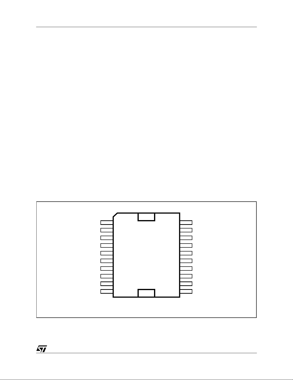
Figure 1. Pin Connection (Top view)
GND GND
OUT3 OUT6
OUT4
OUT5
VS
CLK
DI
VS
OUT1
GND
1
2
3
4
5
6
7
8
9
D99AT455Amod
20
19
18
17
16
15
14
13
12
11
VS
DO
CM
VCC
CSN
VS
OUT2
GND10
3/20

L9949
PIN FUNCTION
N° Pin Description
1, 10,
11, 20
5, 8, 13, 18V
15 V
14 CSN Chip Select Not input:
6CLKSerial clock input:
7 Data In Serial data input:
17 Data Out Serial data output:
16 CM Current monitor output:
GND Ground:
Reference potential
Important:
externally connected !
Power supply voltage (battery):
S
For this input a ceramic capacitor as close as possible to GND is recommended.
Important:
externally connected !
Logic supply voltage:
CC
For this input a ceramic capacitors as close as possible to GND are recommended.
This input is low active and requires CMOS logic levels. The serial data transfer between L9949
and micro controller is enabled by pulling the input CSN to low level. If an input voltage of more
than 9.6V above VCC is applied to CSN pin the L9949 will be switched into a test mode.
This input controls the internal shift register of the SPI and requires CMOS logic levels.
The input requires CMOS logic levels and receives serial data from the microcontroller. The data
is an 16bit control word and the least significant bit (LSB, bit 0) is transferred first.
The diagnosis data is available via the SPI and this tristate-output. The output will remain in
tristate, if the chip is not selected by the input CSN (CSN = high)
Depending on the multiplexer bits 12 and 13 of the Input Data register this output sources an
image of the instant current through the corresponding highside driver with a ratio of 1/10000
For the capability of driving the full current at the outputs all pins of GND must be
For the capability of driving the full current at the outputs all pins of VS must be
9OUT1Halfbridge-output 1:
The output is built by a highside and a lowside switch, which are internally connected. The
output stage of both switches is a power DMOS transistor. Each driver has an internal parasitic
reverse diode (bulk-drain-diode, highside driver from OUT1 to V
OUT1). This output is overcurrent and open load protected.
12 OUT2
2OUT3Halfbridge-output 3:
3OUT4
4OUT5
19 OUT6 Highside-driver-output 6:
Halfbridge-output 2:
The output is built by a highside and a lowside switch, which are internally connected. The
output stage of both switches is a power DMOS transistor. Each driver has an internal parasitic
reverse diode (bulk-drain-diode, highside driver from OUT3 to VS, lowside driver from GND to
OUT3). This output is overcurrent and open load protected.
Halfbridge-output 4:
Halfbridge-output 5:
The output is built by a highside switch and can be used only for a resistive load, because the
internal reverse diode from GND to OUT6 is missing. This highside switch is a power DMOS
transistor with an internal parasitic reverse diode from OUT6 to V
is overcurrent and open load protected.
→ see OUT1 (pin 9)
→ see OUT3 (pin 2)
→ see OUT3 (pin 2)
, lowside driver from GND to
S
(bulk-drain-diode). The output
S
4/20
ABSOLUTE MAXIMUM RATINGS
Symbol Parameter Value Unit
L9949
V
V
CC
VDI VDO
V
CLK
V
CSN
V
CM
I
OUT1,OUT2,
OUT6
I
OUT3,OUT5
Note: All m axim um ra tin gs are a bsol ute r atings . Leav ing the l imi tatio n of any one of thes e val ues m ay c ause an irre vers ibl e dam age of the
integrated circuit!
DC supply voltage -0.3...28 V
S
single pulse t
< 400 ms 40 V
max
stabilized supply voltage, logic supply -0.3 to 6 V
digital input / output voltage -0.3 to VCC + 0.3 V
,
current monitor output -0.3 to VCC + 0.3 V
output current ±10 A
output current ±5 A
ESD PROTECTION
Parameter Value
All pins
output pins: OUT1 – OUT6
(1) HBM according to MIL 883C, Methode 3015.7 or EIA/JESD22-A114-A
(2) HBM with all unzapped pins grounded
±2
±4
(1)
(2)
kV
kV
THERMAL DATA
Symbol Parameter Value Unit
Operating junction temperature:
T
Temperature warning and thermal shutdown:
Symbol Parameter Min. Typ. Max. Unit
T
jTW ON
T
jTW OFF
T
jTW HYS
T
jSD ON
T
jSD OFF
T
jSD HYS
Operating Junction Temperature -40 to 150 °C
j
Temperature Warning Threshold
Tj increasing 150 °C
Junction Temperature
Temperature Warning Threshold
Tj decreasing 120 °C
Junction Temperature
Temperature Warning Hysteresis 10 K
Thermal Shutdown Threshold
Tj increasing 180 °C
Junction Temperature
Thermal Shutdown Threshold
Tj decreasing 150 °C
Junction Temperature
Thermal Shutdown Hysteresis 10 K
5/20
L9949
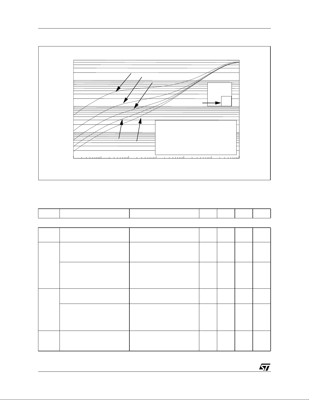
Figure 2. Thermal Data of Package
Z (˚C/W)
th
PowerSO20 Z
th(j-a)
1x1 sq. mm
2x2 sq. mm
3x3 sq. mm
silicon
diss. area dimensions
10
diss. area
1
die size 6x6 sq. mm
0.1
4x4 sq. mm
5x5 sq. mm
mounted on standard board
T = 20˚C
amb
still air
dissipated power 1 W - single pulse
diss. area located in a corner
0.001 0.01 0.1
1
10 100 1000
Time (s)
ELECTRICAL CHARACTERISTCS
VS=8to16V, VCC= 4.5 to 5.5 V, Tj= -40 to 150 °C, unless otherwise specified. The voltages are refered to
GND and currents are assumed positive, when the current flows into the pin
Symbol Parameter Test Condition Min. Typ. Max. Unit
.
Supply
V
I
I
S+ICC
Operating Supply Voltage
S
Range
I
DC Supply Current active mode,
S
Quiescent Supply Current standby mode,
DC Supply Current active mode, CSN = VCC,
CC
Quiescent Supply Current
Sum Supply Quiescent Current standby mode, CSN = VCC,
=16V, VCC= 5.3 V,
V
S
OUT1 - OUT6 floating
V
=16V, VCC=0V,
S
T
j
OUT1 - OUT6 floating
V
S
standby mode, CSN = VCC,
VS=16V
T
j
OUT1 - OUT6 floating
VS=16V, VCC= 5.3 V, Tj<85°C
OUT1 - OUT6 floating
(1)
<85°C
=16V; VCC= 5.3 V
, VCC= 5.3V,
(1)
<85°C
728V
720mA
612µA
12mA
40 75 µA
50 90 µA
6/20
 Loading...