

QUAD HALF-BRIDGEAND SINGLE HIGH-SIDE DRIVER
LOW CONSUMPTION IN STANDBY MODE
(<100µA AT ROM TEMP; < 150µA AT130°C)
TWOHALFBRIDGESFOR3ALOAD
(R
TWOHALFBRIDGESFOR0.5ALOAD
(R
HIGHSIDE DRIVER FOR 2.5ALOAD
(R
DIRECT CONTROLLED BYµC (MULTIPLEX
SYSTEM)
OUTPUTHIGH/LOW LEVELDIAGNOSTIC
OVERCURRENT SWITCH OFF AND DIAG-
NOSTIC
OVERTEMPERATURE DIAGNOSTIC BE-
FORE SWITCH OFF
OPENLOAD DIAGNOSTIC
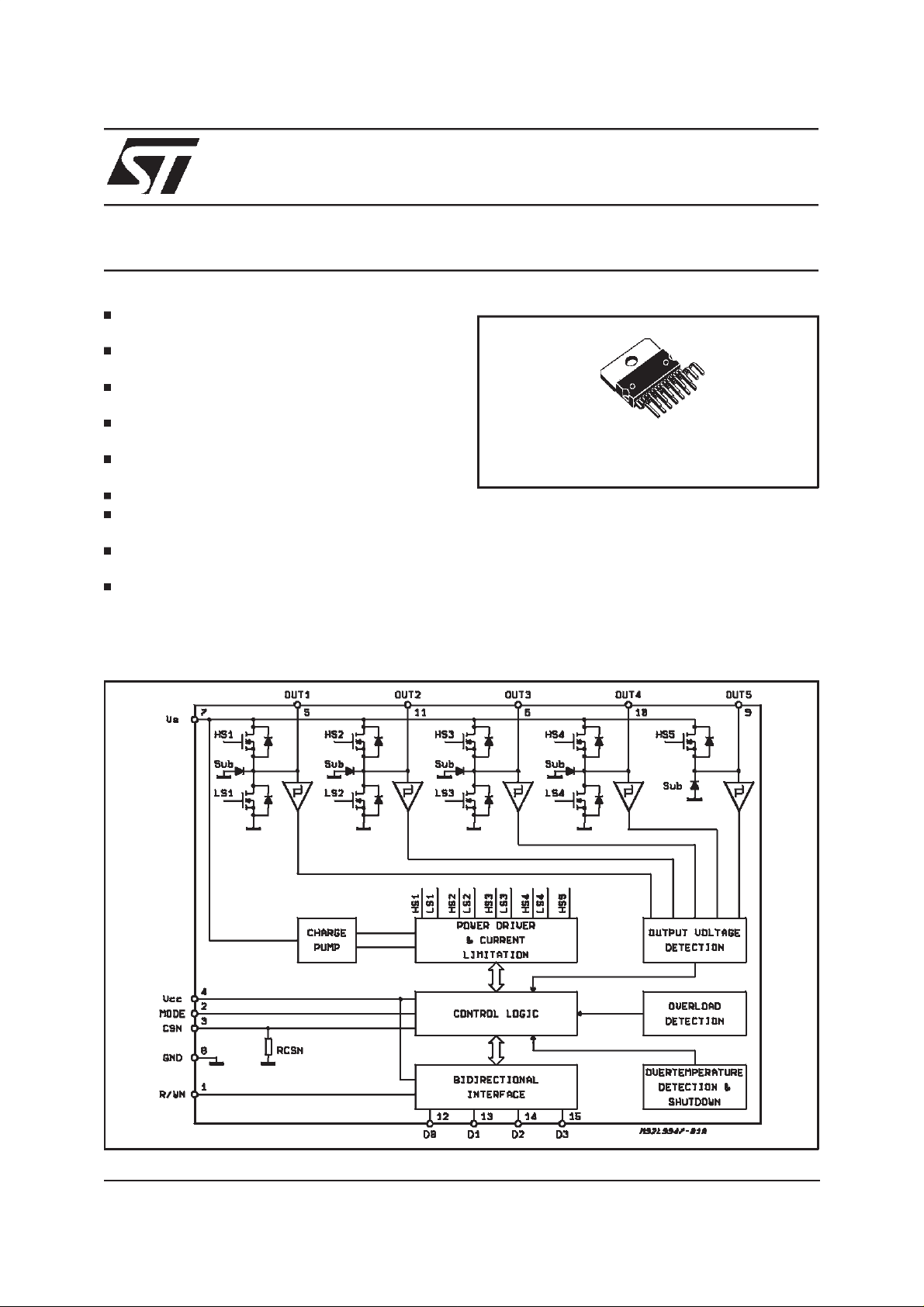
DESCRIPTION
The L9947 is a bus controlled power interface in-
=0.25Ω TYP;Tj=25°C)
DSON
=2.5Ω TYP;Tj=25°C)
DSON
=0.45Ω TYP; Tj=25°C)
DSON
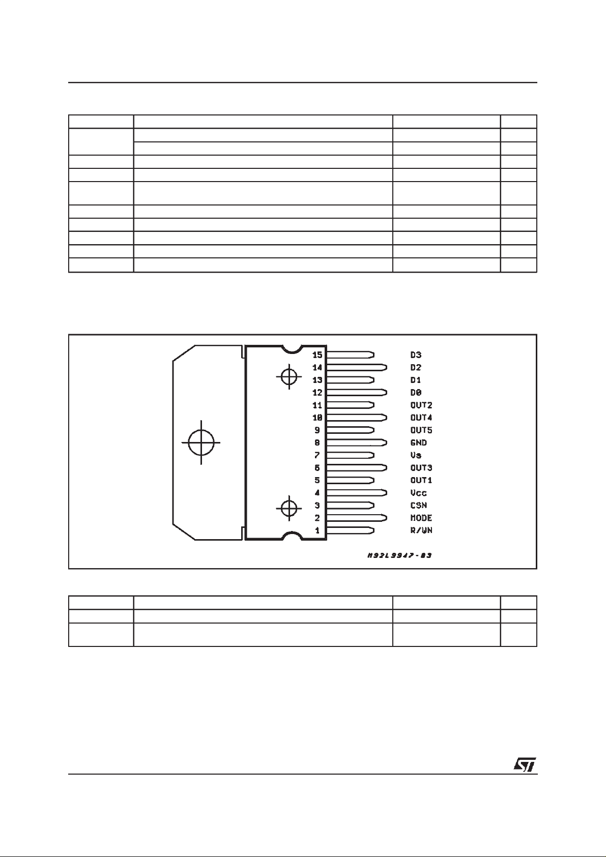
L9947
Multiwatt 15
ORDERING NUMBER:
tended for automotive applications realized in
multipower BCD60II technology. Up to three DC
motors and one grounded resistive load can be
driven with its four half-bridge and one high-side
driverpower outputs. The microcomputer compatible bidirectional parallel bus allows several interfaces connected on the same bus (multiplex system). The full diagnosticinformation is available on
thebus.
L9947S
BLOCK DIAGRAM
April 1999
1/13
L9947
ABSOLUTE MAXIMUM RATINGS
Symbol Parameter Value Unit
V
S
I
S
V
CC
V
CSN,VR/WN
V
MODE
V
D0 -D3
I
OUT1 - OUT5
T
j
T
j-SD
T
j-HYS
PIN CONNECTION
DC Supply Voltage 26 V
Single Pulse t
< 400ms 40 V
max
Negative Supply Current -9 A
Stabilized Supply Voltage -0.3 to 6V V
Digital Input Voltage -0.3 to VCC+0.3 V
Digital Input/ Output Voltage -0.3 to VCC+0.3 V
Output Current Power internal limited
Operating Junction Temperature -40 to 150
Thermal ShutdownJunction Temperature min 150
Thermal JunctionTemperature Hysteresis 20 K
C
°
C
°
THERMAL DATA
Symbol Parameter Value Unit
2/13
R
th j-amb
Z
th j-amb
Thermal ResistanceJunction AmbientP
Thermal ResistanceJunction Ambientstill air;
single pulse tp=20s
= 25W; free air; DC 38 °C/W
tot
10 °C/W
L9947
ELECTRICAL CHARACTERISTICS
= 8 to 16V; VCC= 4.5 to 5.5V; Tj= -40 to 150°C;unless other-
(V
S
wise specified; the voltage are refered to GND and currents are assumed positive, when the current
flows into the pin.)
SUPPLY:
Symbol Parameter Test Condition Min. Typ. Max. Unit
CC DC Supply Current V
I
= 16V; VCC= 5.5V; (status
S
5mA
8)
I
S
DC Supply Current VS= 16V; VCC= 5.5V; (status
10 mA
8)
I
CC + I
Sum Supply Current I
S
OUT1=IOUT2=IOUT3=IOUT4 =
I
= 0; Standby (status 2)V
OUT5
S
100 µA
= 14V; VCC= 5.5V;
T
= -40 to 25°C
j
I
OUT1=IOUT2=IOUT3=IOUT4 =
I
= 0; Standby (status 2)V
OUT5
S
150 µA
= 14V; VCC= 5.5V;
T
>25°C
j
< 14V; VCC= 5.5V; I
V
S
OUT
=0;
3mA
(status 17);
V
SOVT
Overvoltage Shutdown
17 25 V
Threshold
CONTROLINPUTS: CNS, R/WN, MODE
Symbol Parameter Test Condition Min. Typ. Max. Unit
V
V
V
INL
INH
INHyst
I
INL
I
INH
Input Low Level VCC= 5V 1.5 V
Input High Level VCC= 5V 3.5 V
Input Hysteresis VCC= 5V; 0.5 V
Input Current Low VCC= 5V; VIN= 0 -10 10 µA
Input Current High (with
VCC= 5V; VIN= 5V -10 10 µA
exception of CSN Input)
R
CSN
Input Resistance to GND (pull
20 KΩ
down at CSN pin)
DATA INPUT: D0 - D3
Symbol Parameter Test Condition Min. Typ. Max. Unit
V
V
V
DINHyst
I
DINL
I
DINH
DINL
DINH
Input Low Level VCC= 5V; MODE = 0 1.5 V
Input High Level VCC= 5V; MODE = 0 3.5 V
Input Hysteresis VCC= 5V; MODE = 0 0.5 V
Input Current Low VCC= 5V; VIN= 0 -10 10 µA
Input Current High VCC= 5V; VIN= 5V -10 10 µA
DATA OUTPUT:D0 - D3
Symbol Parameter Test Condition Min. Typ. Max. Unit
V
V
DOL
DINH
Output Low Level VCC= 5V; ID= 0.5mA; MODE
=1
Input High Level VCC= 5V; ID= 0.5mA; MODE
=1
4V
0.6 V
3/13
L9947
ELECTRICALCHARACTERISTICS
(continued)
OUTPUTS:
Symbol Parameter Test Condition Min. Typ. Max. Unit
R
ON OUT1
On Resistance to Supplyor
GND
R
ON OUT2
On Resistance to Supplyor
GND
R
ON OUT3
On Resistance to Supplyor
GND
R
ON OUT4
On Resistance to Supplyor
GND
R
ON OUT5
|I
OUT1
On Resistance to Supply VS=8V; Tj= 125°C; I
| Output Current Limitation to
Supply or GND
|I
| Output Current Limitation to
OUT2
Supply or GND
|I
| Output Current Limitation to
OUT3
Supply or GND
|I
| Output Current Limitation to
OUT4
Supply or GND
|I
| OutputCurrentLimitation to GND 2.5 7.5 A
OUT5
I
OUT1
I
OUtT2
I
OUT3
I
OUT4
I
OUT5
V
OUT1-5
Output Current V
Output Current V
Output Current V
Output Current V
Output Current V
Output Voltage Detection
Thresholds
T
JOT
Overtemperature Detection
Thresholds
t
f
OSC
ISC
Overcurrent Switch off Time 50
Internal Oscillator Frequency 250 KHz
VS=8V; Tj= 125°C;
I
= ±0.5A
OUT
>10V; Tj =125°C;
V
S
I
=± 0.5A
OUT
VS=8V; Tj= 125°C;
I
= ±0.5A
OUT
> 10V; Tj=125°C;
V
S
I
=± 0.5A
OUT
VS=8V; Tj= 125°C;
I
= ±2.5A
OUT
> 10V; Tj=125°C;
V
S
I
=± 2.5A
OUT
VS=8V; Tj= 125°C;
I
= ±2.5A
OUT
>10V; Tj=125°C;
V
S
I
=± 2.5A
OUT
= -2A 1.0 Ω
OUT
> 10V; Tj=125°C;
V
S
I
= -2A
OUT
For the function of the short
0.67 2 A
6 Ω
3.95 Ω
6 Ω
3.95 Ω
600 mΩ
395 mΩ
600 mΩ
395 mΩ
0.7 Ω
circuit current limitation see the
functional description (pag....)
0.67 2 A
412A
412A
=2.5V;(status 18) 5 15 mA
OUT1
=2.5V;(status 18) 5 15 mA
OUT2
=2.5V;(status 18) 5 15 mA
OUT3
=2.5V;(status 17) 80 500 mA
OUT4
V
OUT4=VS
OUT5=VS
-2.5V;(status 16 or 18) -80 -500 mA
-2.5V;(status 18) -5 -15 mA
VS=13V; (status 11)
4.9
LOW
HIGH
HYSTERESIS
7.5
0.4 V
0.6 V
0.2 V
5.5
S
8.1
S
S
status 12 - 15 130 °C
steady state t >20ms 125 <T
JSD
°C
µ
V
V
V
s
4/13
 Loading...