

TWO-PHASESTEPPER MOTOR DRIVER
2 X 1.1A FULLBRIDGEOUTPUTS
INTEGRATEDCHOPPINGCURRENT REGU-
LATION
MINIMIZED POWER DISSIPATION DURING
FLYBACK
OUTPUT STAGES WITH CONTROLLED
OUTPUT VOLTAGE SLOPES TO REDUCE
ELECTROMAGNETICRADIATION
SHORT-CIRCUIT PROTECTION OF ALL
OUTPUTS
ERROR-FLAG FOR OVERLOAD,OPENLOAD
ANDOVERTEMPERATURE PREALARM
DELAYED CHANNEL SWITCH-ON TO REDUCE PEAK CURRENTS
MAX.OPERATINGSUPPLYVOLTAGE24V
STANDBYCONSUMPTIONTYPICALLY40µA
SERIALINTERFACE (SPI)
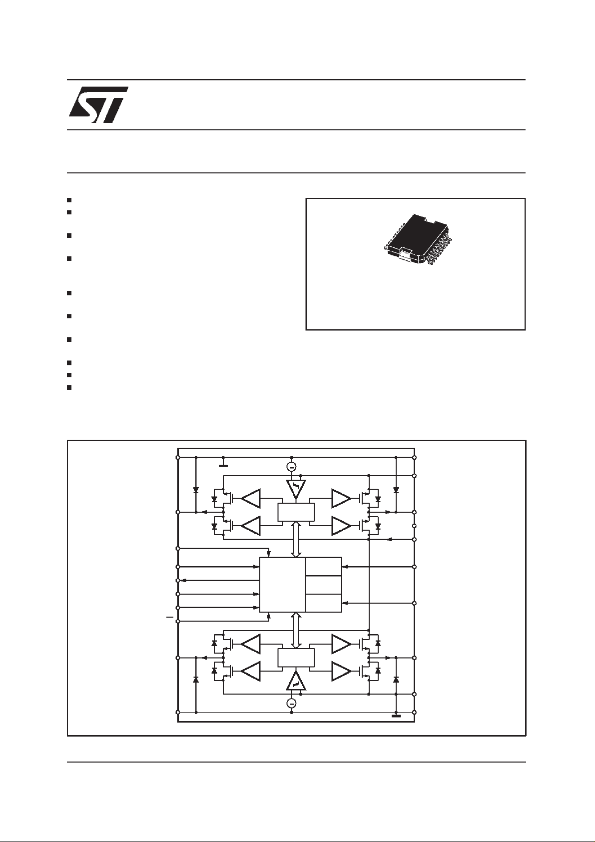
BLOCK DIAGRAM
L9935
PowerSO20
ORDERING NUMBER: L9935
DESCRIPTION
The L9935 is a two-phase stepper motor driver
circuit suited to drive bipolar stepper motors. The
device can be controlled by a serial interface
(SPI). All protections required to design a well
protected system (short-circuit, overtemperature,
cross conduction etc.) are integrated.
OUT
OUT
GND
SCK
SDI
SDO
VCC
CSN
GND
201
~
2
A1
3
4
5
6
7
8
EN
9
B1
10
DRIVER
COMMON
LOGIC
DRIVER
LOGIC
OSCILLATOR
DIAGNOSTIC
BIASING
LOGIC
~
19
18
17
16
15
14
13
12
11
D99AT415
GND
SR
OUT
N.C.
V
OSC
C
OUT
SR
GND
A
A2
S
DRV
B2
B
November 1999
1/19
L9935
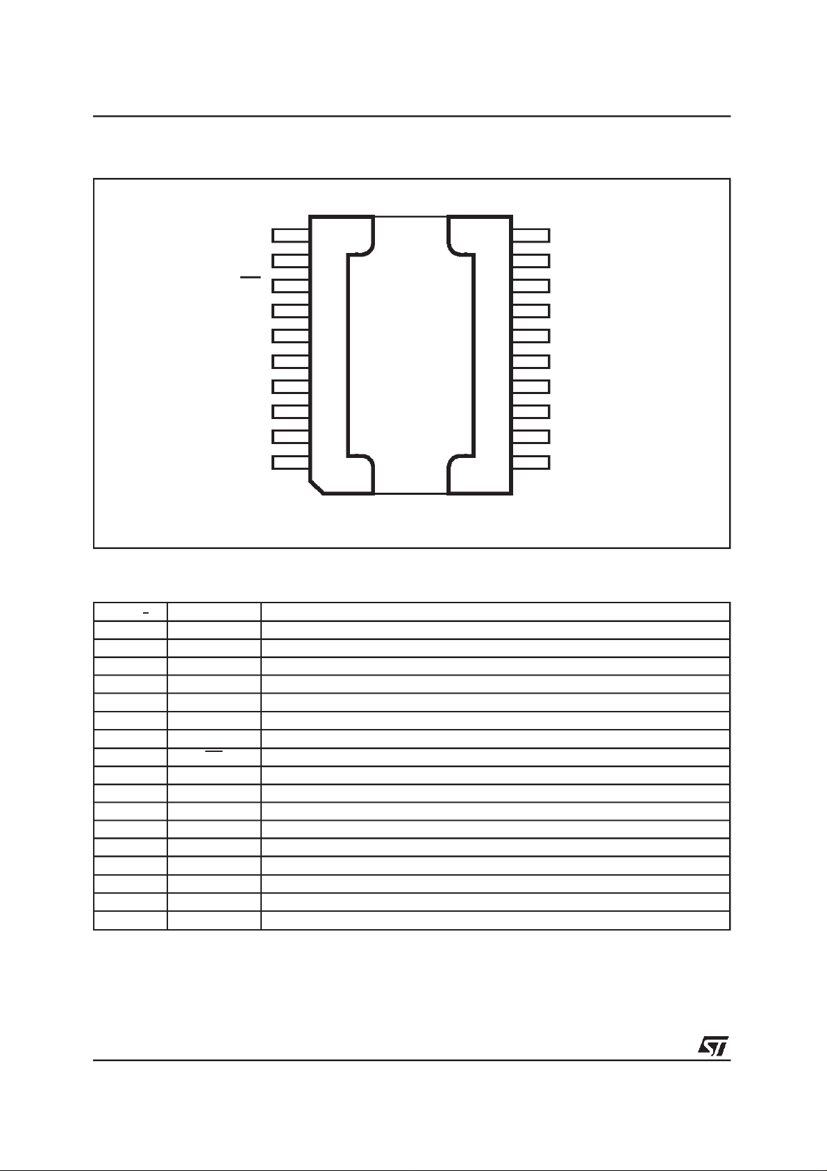
PIN CONNECTION
GND
OUT
B1
EN
CSN
VCC
SDO
SDI
SCK
OUT
A1
GND GND
10
9
8
7
6
5
4
3
2
1
D99AT416
11
12
13
14
15
16
17
18
19
20
GND
SR
OUT
C
DRV
OSC
V
S
N.C.
OUT
SR
B
B2
A2
A
PIN FUNCTIONS
o
Pin N
1,10,11,20 GND Ground. (All ground pins are internally connected to the frame of thedevice).
2 OUT
3 SCK Clock for serial interface (SPI)
4 SDI Serial data input
5 SDO Serial data output
6 VCC 5V logic suplly voltage
7 CSN Chip select (Low active)
8 EN Enable (Low active)
9 OUT
12 SR
13 OUT
14 C
15 OSC Oscillator capacitor or external clock
16 VS Supply voltage
17 NC Not connected
18 OUT
19 SR
Name Description
A1
B1
B
B2
DRV
A2
A
Output 1 of full bridge 1
Output 1 of full bridge 2
Cyrrent sense resistor of the chopper regulator for OUT
Output 2 of full bridge 2
Charge pump buffer capacitor
Output of full bridge 1
Current sense resistor of the chopper regulator for OUT
B
A
2/19

L9935
ABSOLUTE MAXIMUM RATINGS
Symbol Parameter Value Unit
V
S
V
SPulsed
V
OUT (Ai/Bi)
I
OUT (Ai/Bi)
V
SRA/SRB
V
CC
V
CDRV
V
SCK,VSDI
V
CSN,VEN
V
OSC,VSDO
Note: ESD for allpins, except pins SDO, SRA and SRB, areaccording to MIL883C, tested at 2kV, corresponding to a maximum energy
dissipation of 0.2mJ. SDO, SRA and SRB pins are tested with800V.
THERMAL DATA
Symbol Parameter Value Unit
R
th j-case
R
th j-amb
R
th j-amb,FR4
T
S
T
SD
DC Supply Voltage -0.3 to 35 V
Pulsed supply voltage T < 400ms -0.3 to 40 V
Output Voltages internally clamped to V
or GND depending on the
current direction
DC Output Currents
Peak Output Currents (T/tp ≥ 10)
1.2
±
±2.5
Sense Resistor Voltages -0.3 to 6.2 V
Logic Supply Voltages -0.3 to 6.2 V
Charge Pump BufferVoltage versus V
,
Logic Input Voltages -2 to 8 V
S
-0.3 to 10 V
Oscillator Voltage Range, Logic Output -0.3 to VCC+0.3 V
Typical Thermal Resistance Junction to Case 5 °C/W
Typical Thermal Resistance Junction to Ambient
2
(6cm
Ground Plane 35µm Thhickness)
Typical Thermal Resistance Junction to Ambient
35 °C/W
8 °C/W
(soldered on a FR 4 board with through holes for heat transfer
and external heat sink applied)
Storage Temperature -40 to 150 °C
Typical Thermal Shut-Down Temperature 180 °C
S
A
A
ELECTRICALCHARACTERISTICS
erwise specified.)
1)
(8V ≤ V
≤ 24V; -40°C ≤ Tj≤ 150°C; 4.5V ≤ VCC≤ 5.5V, unless oth-
S
Symbol Parameter Test Condition Min. Typ. Max. Unit
SUPPLY
IS
I
SOP
I
CC
85
Total Supply Current
I
S+IVCC
(BothBridges Off)
Operating Supply Current I
5V Supply Current EN = LOW 1.4 10 mA
= 14V
V
S
EN = HIGH
T
≤ 85°C
J
=0
OUT Ai/Bi
f
= 30kHz
OSC
V
= 14V
S
40 100
4.5 mA
FULL BRIDGES
R
OUT, Sink
R
OUT, Source
R
OUT8, Sink
V
FWD
V
REV
t
r,tf
R
of Sink Transistors Current bit
DSON
RDSON of Source Transistors 0.4 0.7 Ω
RDSON of Sink Transistors +
R
of SourceTransistors
DSON
Forward Voltage of the DMOS
Body Diodes
combinations LL, LH,
V
12V
≥
S
Current bit
Combinations LL, LH,
V
=8V
S
EN = HIGH
I
= 1A; VS≥ 12V
FWD
Reverse DMOS Voltage EN = LOW
I
=1A
REV
Rise and Fall Time of Outputs
OUT
Ai/Bi
0.1...0.9 V
OUTVS
Chopping 550mA
= 14V
0.3 0.6 1.5
0.4 0.7 Ω
1.6 3 Ω
1 1.4 V
0.5 0.9 V
A
µ
s
µ
3/19
L9935
ELECTRICALCHARACTERISTICS
(continued)
Symbol Parameter Test Condition Min. Typ. Max. Unit
R
SWITCH OFF THRESHOLD OF THE CHOPPER (R
2)
V
V
V
SRHL
SRLH
SRLL
Voltage Drops Across R1⋅ R
(Voltage at Pin SRAor SRBvs.
GND)
Bit 5, 2 = H Bit 4, 1 = L 12 20 35 mV
2
Bit 5, 2 = L Bit4, 1 = H 160 180 210 mV
Bit 5, 4, 2, 1 = L 270 300 340 mV
1
⋅
= 0.33Ω)
2
ENABLE INPUT EN
V
EN High
High Input Voltage V
CC
V
-1.2V
V
EN low
V
EN Hyst
I
EN High
I
EN Low
Low Input Voltage 1.2 V
Enable Hysteresis 0.1 V
High Input Current V
High=VCC
Low Input Current VLOW = 0V -3 -10 -30
-10 0 10
µ
µ
A
A
LOGIC INPUTS SDI. SCK, CSN
V
V
V
I
HIGH
LOW
Hyst
HIGH
I
Low
High Input Voltage EN = LOW 2.6 8 V
Low Input Voltage -0.3 1 V
Hysteresis 0.8 1.2 1.6 V
High Input Current V
Low Input Current V
High=VCC
= 0V -3 -10 -30 µA
Low
-10 0 10 µA
LOGIC OUTPUTS (SDO)
V
SDO,High
High Output Voltage I
= -1mA VCC-1 V
SDO
CC
V
CC
V
-0.17
V
SDO,Low
Low Output Voltage ISDO = 1mA 0.17 1 V
OSCILLATOR
V
OSC, H
V
OSC, L
I
f
t
OSC
OSC
Start
High Peak Voltage EN = LOW 2.2 2.46 2.6 V
Low Peak Voltage EN = LOW 1 1.23 1.4 V
Charging/Discharging Current 45 62 80 µA
Oscillator Frequency C
Oscillator Startup Time EN = High→Low 2/f
= 1nF 20 25 31 kHz
OSC
osc
5/f
osc
8/f
osc
THERMAL PROTECTION
T
J-OFF
Thermal Shut-Down
160 180 200 °C
Temperature
T
J-ALM
∆T
MGN
1) Parameters are tested at 125°C. Values at 140°C are guaranteed by design and correlation.
2) Currents of combinations LH and LL are sensed at the external resistors. The Current of bit combination HL is sensed internally and
cannot be adjusted by changing the sense resistors.
Thermal Prealarm 130 160 °C
Margin Prealarm/Shut-Down 10 20 30 K
4/19
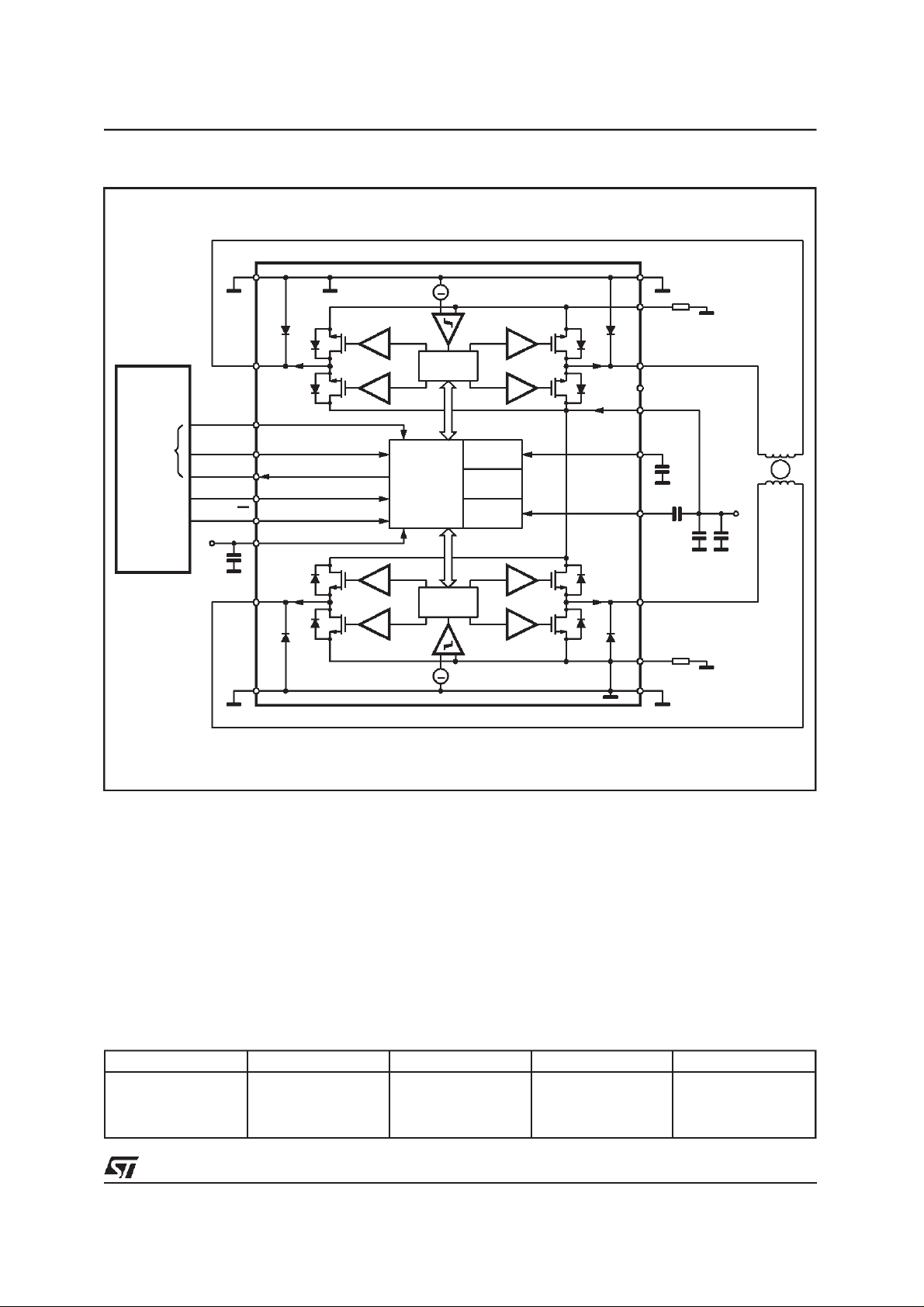
Figure1. General ApplicationCircuit Proposal.
GND 201 GND
2
OUT
SCK
A1
3
DRIVER
~
LOGIC
19 SR
18
17
16
OUT
N.C.
V
S
L9935
A
R1 0.33Ω
A2
+5V
100nF
SDI 4
SDO 5
CSN 7
EN 8
VCC 6
OUT
B1
GND 10
COMMON
LOGIC
9
SDI
INTERFACE
µC
Applicationhints:
C1 and C2 should be placed as close to the device as possible. Low ESR of C2 is advantageous. Peak currents through C1 and C2 may
reach 2A. Care should be taken that the resonance of C1, C2 together with supply wire inductances isnot the choppingfrequencyor a multiple
of it.
FUNCTIONAL DESCRIPTION
Basic structure
The L9935 is a dual full bridgedriver for inductive
Table 1.
15 OSC
14
C
DRV
13 OUT
12 SR
11 GND
C
OSC
1nF
C
Driver
100nF
C1
100nF
B2
B
R2 0.33Ω
D99AT417
DRIVER
LOGIC
~
OSCILLATOR
DIAGNOSTIC
BIASING
loads with a choppercurrentregulation.
Outputs A1and A2 belongto full bridge A
Outputs B1and B2 belongto full bridge B
The polarity of the bridges can be controlled by
bit0 and bit3 (for full bridge A, bit3, for full bridge
B, bit0). Bit5, bit4 (for full bridge A) and bit2, bit1
(for full bridge B) control the currents. Bit3 high
leads to output A1 high. Bit0 high leads to output
B1 high.
Current setting Table 1 using a 0.33W sense resistor.
STEPPER
MOTOR
POWER
SUPPLY
C2
10µF
bit5, bit2 bit4, bit1 IQX(Typ.) I
H
H
L
L
H
L
H
L
0
60mA
550mA
900mA
RX/max
0%
61%
100%
Remark
inernally sensed
5/19
L9935
Figure 2. Typical average load current dependence on R
I
A
1.8
1.1
1
0.8
0.6
0.4
0.2
0.075
0
0 0.1 0.2 0.3 0.4 0.5 0.6 0.7 0.8 0.9 1.0 1.1 1.2 1.3 1.4 1.5 1.6
typical current limitation of high side transistor
limit recommended for usual application
suggested range of operation
Sense
I
LL
I
LH
I
HL
.
D99AT418
R
Ω
Full Bridge Function
Figure 3. Displays a full bridge including the current sense circuit.
M
11
11
M
12
COMP1
+
D
11
A
1
12
D
12
LOAD
D
21
A
D
22
6/19
bit3, (bit0)
bit5, (bit2)
bit4, (bit1)
DRIVE
LOGIC
τ
CURRENT
LOGIC
INHIBIT
ON HH
CURRENT ADJUST
D
D
M
21
2
M
22
R
1
R1EXTERNAL
SENSE RESISTOR
D
21
D
22
D99AT419
V
S

L9935
No current:
Bit 5, bit 4 (correspondingbit 2 and bit1 for bridge
B) both are HIGH, the current logic will inhibit all
drivers D
M
21,M22
11,D12,D21,D22
independentlyfrom the signal of the cur-
turning off M11,M12,
rent sense comparator comp 1.
Turningon:
Changing bit 5 or bit 4 or bothto LOW will turn on
either M
and M22or M21and M12(dependingon
11
the phase signal bit 3). Current will start to flow
through the load. The current will be sensed by
the drop acrossR
.
1
The threshold of the comparator comp1 depends
on the currentsettings of bit 5 and bit 4.
The current will rise until it exceeds the turn off
thresholdof comp 1.
Chopping:
Exceeding the threshold of comp 1 the drive logic
will turn off the sink transistor (M
or M22). The
12
sink transistor periodically is turned on again by
the oscillator. Immediately after turning on M
M
the comparator comp 1 will be inhibited for a
22
12
or
certain time to blank switch over spikes caused
by capacitiveload componentsup to 5 nF.
Turning off for example M
current through D
. (So now the free wheeling
11
will yield a flyback
12
current flows through M21, the load and D11).
This leads to a slow currentdecay during flyback.
Maximum duty cycles of more than 85% (at f
OSC
= 25kHz) are possible. In this case current flows
of both bridges will overlap(not shown in Fig. 5).
Reversingphase:
Suppose the current flowed via M
M
before reversing phase. Reversing phase
12
and M12will be turned off. So now the cur-
M
21
rent will flow through D
, the load and D11. This
22
, the load and
21
leads to a fastcurrent decay.
Chopper control by oscillator
Both chopping circuits work with offset phase.
One chopper will switch on the bridge at the
maximum voltage of the oscillator while the other
chopper will switch on the bridge at minimum
voltage of the oscillator.
MS1 and MS2 blank switching spikes that could
lead to errorsof the current control circuit.
Figure 4. Principal chopper control circuit.
OSC
C
OSC
OSCILLATOR
=
f
OSC
2.46V · C
i
OSC
OSC
RES1
RES2
MS1
RESET
DOMINANT
R
RSFF1
S
S
RSFF2
R
RESET
DOMINANT
Comp1
Dr1
Dr2
MOS DRIVERS
Comp2
inhibit
+
-
+
-
inhibit
SR
SR
A
B
MS2
D99AT420
7/19

L9935
Figure 5. Pulse diagram to explainoffset chopping.
V
OSC
V
SRA
V
SRB
total current consumption
current
threshold 1
current
threshold 2
turn off delay
due to slope
velocity control
I
VS
∆I
D99AT421
Using offset chopping the changes of the supply current remain half as large as using non offset chopping.
Turning off the oscillator for example by shorting pin OSC to ground will hinderturning on of the bridges
anymoreafter the comparatorshavegenerateda turn off signal.
External clocking is possible overdriving the charge and discharge currents of the oscillator for example
with a push pull logic gate. So severaldevices can be synchronized.
Protectionand Diagnosis Functions
The L9935 provides several protection functionsand error detection functions. Current limitation usually
is customer defined by the external current sense resistors. The current sensedthere is used to regulate
the current through the steppermotorwindingsby pulse width modulation.This PWM regulation protects
the sink transistors. The source transistorsare protected by an internalovercurrent shut down turning off
the source transistorsin case of overload.
Overloaddetectionof the source transistor will turn off the bridge and set the corresponding errorflag.
To turn on the bridge again a new byte must be written into the interface. (Rising slope of CSN resets
the overload error flag).
Both bridges use the same flags. To locate which bridge is affected by an error the bridges can be
tested individually (One bridge justis turned off to check for theerror in the other bridge).
Short from an Output to the Supply Voltage VS
The current will be limited by the pulse width modulator.The sink transistorwill turn off again after some
microseconds. The transistor will periodically be turned on again by the oscillator 8 times. After having
detected short 8 times the low side transistor will remain off until the next data transfer took place. After
detection of a short to VS we suggest to turn off the corresponding bridge to reduce power dissipation
for at least1ms.
8/19

L9935
Diagnosisof a Short to VS
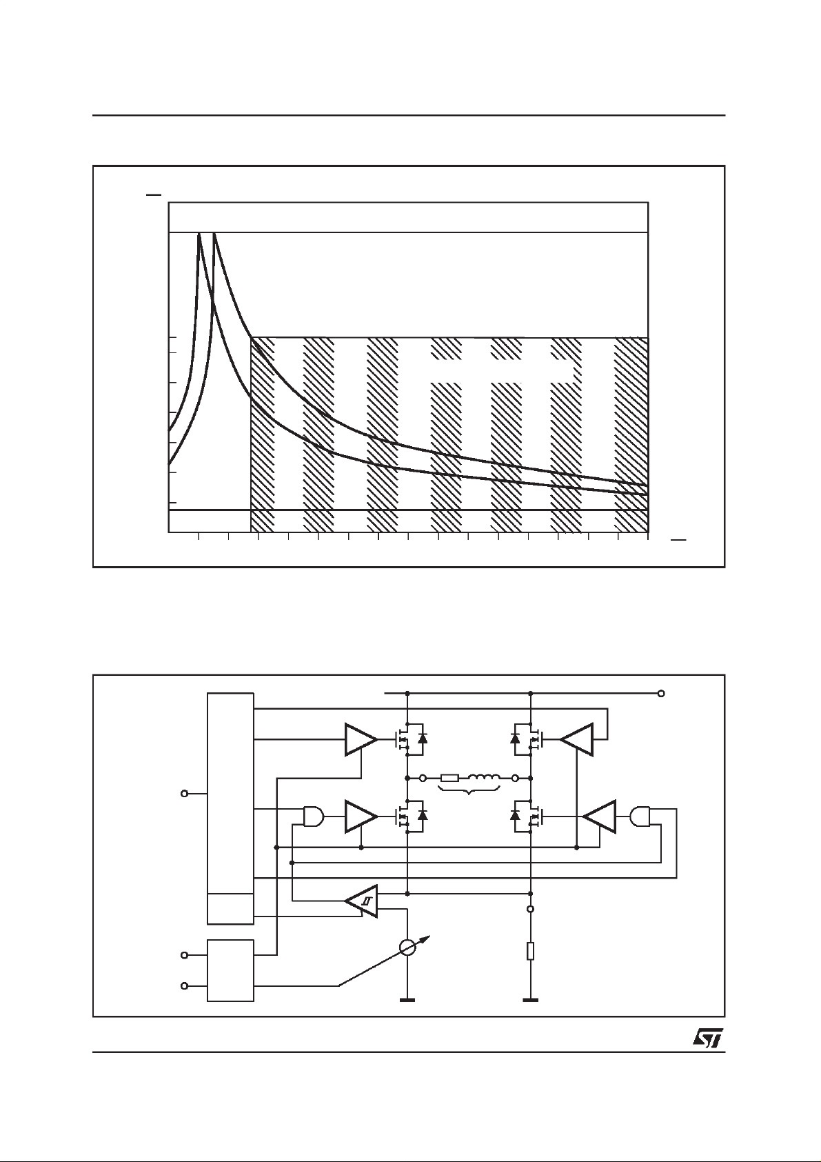
During the short current through the sink transistor will rise more rapidly than under normal load conditions. Reaching a peak current of 1.5 times the maximum PWM current between typically 2µs and 5µs
t
ON
S
t
short
.
t
t
PWM
t
ON
t
short
t
PWM
t
ON
t
short
t
PWM
after turn on will be detectedas a short to V
Detecting a short the low side transistor will try to turn on again the next 7 trigger pulse of the oscillator.
Simultaneouslythe error flag will updated on each pulse.
Figure 6. Normal PWM current versus shortcircuit current and detection of short to VS..
IQshort threshold
PWM threshold
t
t
ON
shorttPWM
PWM
detection
signal (internal)
Short
detection
signal (internal)
Error 1
ton: turn on of the sink
ton+t1=t
ton+t
delay=tPWM
Betweent
Between t
on
short
: activation of short
short
: activation of PWM threshold
and t
and t
the over current detection is totally blanked.
short
the current threshold is set to 1.5 times the maximum PWM current (1.5 times
PWM
transistor
threshold
D99AT422
t
t
t
the current of current setting LL).
Overcurrentnow willset the error flag.
After t
the current threshold is the nominal PWM current set by the external resistor. Exceeding this
PWM
current will just turn off the sink transistor. This is considered as normal operation. The error flag is detachedfrom the comparatorafter tPWM so no error flag is set during normal pulse width modulation.
Short from an Output to Ground
The current throughthe short will be detected by the protection of the source transistor. The source transistor will turn off exceeding a current of typically 1.8A. Minimum overload detection current is 1.2A. To
obtain proper current regulation (by the sink transistors and not by source transistor shut down) the
maximum current of the PWMregulatorshould be set to a maximumvalue of 1.1A.
9/19

L9935
Diagnosisof a Short to Ground
Detecting an overload will set an overcurrent error (Error2 = LOW) (bit6). To reset the error flag a new
byte mustbe written into the interface.(Reset of the error flag takes place at the rising slope of CSN).
ShortedLoad
With a shorted load both, the sink- and the source protection or the PWM alone will respond. In either
case therewill be no flybackpulse.
Diagnosisof a Shorted Load
Shorting the load two events may takeplace:
- overload(of the high side transistor) while low side transistor overcurrent is detectedwill set the
followingcombinations:
bit6 = LOW
bit7 = HIGH
- overloadis marginal. So the low side drivermay turn off before overload is detected.This leads to the
combinationbit6 = HIGH and bit7 = LOW.
Open Load
An open load will not lead to any flyback pulses. Error detection will take advantageof theflyback pulse.
Missingthe flyback pulse after reversingthe polarity of a motor winding bit7 will become LOW.
Open load will not be tested in the low current mode (current bits HL) to avoidthe risk of instable diagnosis at low flayback currents. Open load immediately after reset or power down may on random be detected in the low current mode too. This diagnosishowever will not persist longer than 8 changesof polarity. We strongly suggest to test open load at a high current mode (combination LH or LL).
OvertemperaturePrealarm
Typically 20K before thermal shut down takes place an overtemperature prealarm (bit7 and bit6 low)
takes place. Typicallyovertemperatureprealarmtemperatureis between 150°Cand 160°C.
Applicationhints using a high resistivestepper motor
The L9935 was originally targeted on stepper chopping stepper motor application with typical resistances of 8..12W. Using motors with higher resistance will work too but diagnosisbehaviour will slightly
change. Thisparagraph shows the details that should be taken in account usingdiagnosis for high resistive motors.
Startup behaviour:
The device has simple digital filter to avoid triggering diagnosisat a single event that could be random
noise. This digital filter needs 4 chopping pulses to settle. Using a high resistive motor this chopping
does not take place. Instead the digital filter samples eachtime a polarty change takes place. So the first
three responsetelegramsafter resetmay show an ’open load’ error.
Input data High resistive motor (error bits) Low resistive motor (error bits)
Standby
1st telegram (550mA or 900mA) HH HH
Reverse phase (550mA or 900mA) XH HH
Reverse phase (550mA or 900mA) XH HH
Any data XH HH
Any data HH HH
H means check for HIGH at the error bits.
X means don’t care becausefilter is not yet settled.
10/19

L9935
Using 75mAchoppingimmediatelly after stand by:
The high resistive motor can be forced to chopping operation in the low current range. This leads to the
samebehaviouras using a low resistive motor.
Short to V
The short to VS flag is overwritteneach time the chopper comparator responds. Having detected a short
this flagonly can be reset by reachingchopping operation or resetting the circuit (ENN=1). For a high resistive motor thisleads to the following consequence: Once a short to VS is detected the error flag will
persist even if the short is removed again until either a reset (ENN=1) or chopping(for example in 75mA
mode) has taken place. We suggest to return to operation once a short to VS was detected by using the
low currentmode to reset the flag.
Limitation of the Diagnosis
The diagnosis depends on either detecting an overcurrent of more than typically 1.8A through the
source transistor or on not detecting a flyback pulse, or on detecting severe overcurrents of the sink
transistorimmediatelyafter turn on.
Smallcurrents bypassing the load will not be detected.
In the low current range (hold current) the flyback pulse (especially commutatingagainst the supply
voltage after changing phase) may (depending on the inductivity of the stepper motor windings) be
too short to be detected correctly. For this reason diagnosis using the flyback pulse is blanked at
phase reversalat hold current.
In the low current range (hold current) the current capability of the bridge is reduced on purpose.
Short to VS may not be detected.In stead the bridge may just chop likenormal operation.
Flyback pulse detection is not blanked during PWM regulation at hold current (here commutation
voltage is less than 1V thus providing a longer pulse duration.) This however should be taken in account using stepper motors with low inductivity (less than 0.5mH). Using motors with such a low inductivitythe flybackvoltage in hold mode may decay too fast.
Motors with extremely low ohmic resistance tend to pump up the current because current decay during flyback approaches zero while at bridge turn on the current will increase. This may lead to overcurrent detection. We suggest to use stepper motors with an ohmic resistanceof approximately 3Ω or
more.
Partial shorts of windings or shorts of stepper motors with coils in series may still yield a flyback pulses
that are accepted by the diagnosisas a proper signal.
Table 2. Error table.
detectionusing high resistivemotors:
S
Error 1
bit7
H H Normal operation
L H Shortto VS (sink overload immediately after turn on)
H L short to gnd (source overload, missing flyback is masked)
L L overtemperature prealarm
Error 2
bit6
Description
shorted load (no flyback)
open load (no flyback)
At stepping rates faster than 1ms/data transfer error flags indicating a short should be used to initiate a
pause of at least 1ms to allow the power bridges to cool down again.
11/19

L9935
Serial Data Interface (SPI)
The serial data interface itself consists of the pins SCL (serial clock), SDI (serial data input) and SDO
(serial data output).
To especially support bus controlled applications the additional signals EN (chip enable not) and CSN
(chip select not) are available.
Startup of the Serial Data Interface
Falling slope of EN activatesthe device.After t
Falling slope of CSN indicates start of frame. Data transfer (reading SDI into the register) takes place at
the rising slopes of SCK.
Data transfer of the register to SDO takes placeat the falling slopeof SCK.
Rising slope of CSN indicates end of frame. At the end of frame data will only be accepted if modulo 8
bit (modulo8 fallingslopes to SCK)have been transferred. If this is not the case the input will be ignored
and the bridges will maintain the same status as before.
SDO is a tristateoutput.
SDO is activewhile CSN = LOW, while CSN = HIGH SDO is high resistive.
Figure 7. SPI Data/ClockTiming.
t
en_sck
the device is readyto work.
en.sck
EN
CSN
SCK
SDI
SDO
A
X
CSN
SCK
MSB7 bit6 bit5 bit4 bit3 bit2 bit1 bit0
MSB7 bit6
t
1
t
1
bit5 bit4 bit3 bit2 bit1 bit0
CURRENT AERROR BITS
t
cl
tsut
t
ch
sh
CURRENT B POLARITY BPOLARITY A
t
1
t
Pd
t
1
12/19
SDI
SDO
bit7
td
bit7
bit0
t
zch
bit0
D99AT437

L9935
Test condition for all propagation times (unlessotherwise specified)
HIGH ≥ 3V; LOW ≤ 0.8V; t
Symbol Parameter Test Conditions Min. Typ. Max. Unit
f
SCLK
t
1
SCK-Frequency DC 2MHz
SCK stable before and after
CSN = 0
t
ch
t
cl
t
su
t
sh
t
d
t
zc
t
en_sck
t
pd
(*) Measured at a transitionfrom High impedance (Bridge off) to bridgeon. (Reversing polaritytakes about 1µs longerbecause the bridge first
turns off before turning on in reverse direction).
Width of SCK high pulse 200 ns
Width of SCK low pulse 200 ns
SDI setup time 80 ns
SDI hold time 80 ns
SDO delay time (CL = 50pF) 100 ns
SDO high Z CSN high 100 ns
Setup time ENABLEto SCK HIGH > VCC-1.2V 30 µs
Propagation delay SPI to
output Q
XX
Table of bits
bit5,bit4 : current range of bridge A (OutputsA1 and A2)
bit3 : polarityof bridge A
bit2,bit1 : current range of bridge B (OutputsB1 and B2)
bit0 : polarityof bridge B
bit7,bit6 : Error1and Error 2
=10ns, Enable: ENN Low < 0.8V, ENN High > Vcc-0.8V
r,tf
100 ns
2 (*) µs
Cascading severalDevices
Cascading several devices can be done using the SDO output to pass data to the next device. The
whole framenow consists of n byte. n is the number of devices used.
Figure 8. CascadingSeveral Steppermotor drivers.
no.1 no.2 no.3
SDO
SDOSDI
SDOSDI SDOSDI
µP
SCKCSN CSN
SCK
SCK
CSN
SCK
D99AT438
CSN
Figure 9. Control sequence for 3 Stepper motordrivers.
EN
CSN
SCK
SDO
of µP
Q
byte forno. 3 byte forno. 2 byte forno. 1
XX
D99AT439
13/19

L9935
Figure 10. Paralleling several Devices.
no.1
SDI SDO
SCK
µP
CSN1
CSN2
SDI SDO
SCK
CSN
no.2
SDI SDO
SCK
CSN
D99AT440
here usuallyonly one Steppermotor driver is selected at a time while all others are deselected.
ApplicationInformation
For driving a stepper motor we suggest to use the following codes. The columned ’SDO correct’ shows
the data returned at SDOin correctfunction. The columnes presented under ’Error cases’ display thediagnosis bits if errors are detected.
Examplesof control sequences
Full step mode control sequencesanddiagnosis response.
SDI SDO
bit 76543210 76543210 76 76 76 76 76 76 76 76 76 76 76 76543210
XX111111 SDO PRESENT LAST DATA OR 11111111 IN CASE PREV. STATE WAS STAND BY
XX011011
XX010011
XX010010
XX011010
XX011011
XX010011
XX010010
XX011010
*) Motorresistance approximatelly 10Ω and VS= 12V. So a short to ground only is detected on one branche of thebridge.Lower resistivity of
the motor may lead to detection of short to groundon both branches of the bridge leading to code 10 on all steps.
14/19
correct
11111111
11011011
11010011
11010010
11011010
11011011
11010011
11010010
A
O
P
E
N
11
11
01
11
01
11
01
11
O
N
11
11
11
01
11
01
11
01
B
A1
S
P
H
E
O
R
T
VS
11
11
01
01
01
11
01
01
Error cases and SDObit7, bit6
A1
B2
B1
A2
S
H
O
R
T
VS
11
01
01
11
01
01
01
11
S
H
O
R
T
VS
11
11
11
01
01
01
11
01
S
H
O
R
T
VS
11
01
01
01
11
01
01
01
*)
S
H
O
R
T
GND
11
10
01
11
10
10
01
11
A2
*)
S
H
O
R
T
GND
11
11
10
10
01
11
10
10
B1
*)
S
H
O
R
T
GND
11
10
10
01
11
10
10
01
B2
*)
S
H
O
R
T
GND
11
11
11
10
10
01
11
10
therm.
alarm
00
00
00
00
00
00
00
00
therm.
shut
down
(reset
operating
codes)
00111111
00111111
00111111
00111111
00111111
00111111
00111111
00111111

L9935
These sequences are intended to give the user a good starting point for his software development. Besides these two there are further possibilitieshow to implement control sequences for this device (other
currents,quartersstep etc.).
therm.
B2
B1
A2
A1
B2
B1
A2
A1
O
P
E
N
11
11
11
11
11
01
11
11
11
01
11
11
11
01
11
11
11
O
N
11
11
11
11
11
11
11
01
11
11
11
01
11
11
11
01
11
B
S
S
S
S
H
H
P
E
O
R
T
VS
11
11
11
11
11
01
01
01
01
01
11
11
01
01
01
01
01
O
R
T
VS
11
01
01
01
01
01
11
11
11
01
01
01
01
01
11
11
11
H
O
R
T
VS
11
11
11
11
11
11
11
01
01
01
01
01
11
11
11
01
01
H
O
R
T
VS
11
11
11
11
01
01
01
01
11
11
11
01
01
01
01
01
11
GND
*)
H
O
R
11
10
10
10
10
01
11
11
11
11
10
01
10
01
11
11
11
*)
S
S
H
O
R
T
T
GND
GND
11
11
11
11
11
11
10
10
10
01
11
11
11
11
10
10
10
11
11
11
11
10
10
10
01
11
11
11
11
10
10
10
01
11
*)
*)
S
H
O
R
T
S
H
O
R
T
GND
11
11
11
11
11
11
11
11
10
10
10
01
11
11
11
11
10
alarm
00
00
00
00
00
00
00
00
00
00
00
00
00
00
00
00
00
SDI SDO A
bit 76543210 76543210 76 76 76 76 76 76 76 76 76 76 76 76543210
XX111111
XX011111
XX011111
XX011111
XX011011
XX111011
XX010011
XX010111
XX010010
XX110010
XX011010
XX011110
XX011011
XX111011
XX010011
XX010111
XX010010
XX110010
previous code
11111111
11011111
11011111
11011111
11011111
11011011
11111011
11010011
11010111
11110010
11011010
11011110
11011011
11111011
11010011
11010111
11010010
therm.
shut
down
(reset
operating
codes)
00111111
00111111
00111111
00111111
00111111
00111111
00111111
00111111
00111111
00111111
00111111
00111111
00111111
00111111
00111111
00111111
00111111
Double errors: Double errors will create composite codes by an AND operation between columns of the
same dominance.Openand short to VS are the least dominant error codes. (first 6 error code columns).
Short to ground is the second dominant error code. detection of short to gnd will overwriteerror codes of
the least dominant kind (open, short to VS). Temperature prealarm and thermal shut down are the most
dominant error codes. Thermal prealarm returns error code 00 but the device stillis working and returns
the appropriateoperationcode (bits 0..5).
Thermal shutdown returnserror code 00 and turns off the device. The opcode returnedcorresponds the
action eventuallyperformed(bit 0..5 become 1).
For example open bridge A and simultaneously open bridge B will lead to error code 01 by performing
an AND operation betweenthe two correspondingcolumns.
*) Motorresistance approximatelly 10Ω and VS= 12V. So a short to ground only is detected on one branche of thebridge.Lower resistivity of
the motor may lead to detection of short to groundon both branches of the bridge leading to code 10 on all steps.
ElectromagneticEmission classification(EME)
Electromagnet i cEmiss i on classes presentedbelow are typical data found on benchtest. For detailedtest descriptionpleasereferto’ElectromagneticEmission (EME) Measurementof IntegratedCircuits, DC to 1GHz’ of
VDE/ZVEIworkgroup767.13andVDE/ZVEIworkgroup767.14or IECprojectnumber 47A1967Ed.This data
is targetedto boarddesignerstoallowanestimati onof emissi onfiltering effortrequi redinapplic ati on.
Pin EME class Remark
GND E 10 0 1Ωtest
V
CC
EN. SDI, CSN, CSK, SDO in tristate K h
SDO G f SDO in low-Z state, nodata transfer
Power output A
Power output A
1,A2,B1,B2
1,A2,B1,B2
E e Blocked with 100nFclosemto the device
E 5 f Sourcing output
6 f Sinkingoutput in chopping mode f
osc
=20kHz
ElectromagneticEmissionis not testedin production.
15/19

L9935
Figure 11. State diagram.
ST
AND
BY
turn on
DEVICE
CHECKS
ERRORS 11
short
to VS
OFF OFF
new
telegram
CHECKING
FOR
ERRORS
short to VS
ON
FOR
shor
to
shor
to VS
01
short to VS
new telegram
no error
t
to
VS
t
t
shor
no short
same polarity as before
shor
t
gnd
gnd
to
new
telegram
CHECKING
FOR
ON
ERRORS
11
10
short
to gnd
new telegram
same polarity
new telegram current = 0
shor
t
to gnd
no short
LOGIC
SELECTS
BRANCHE
DEPENDING
ON
PREVIOUS
STATE
new telegram
flyback OK
or reverse polarity
shor
t
to
gnd
different polarity
than before
ON
CHECKING
FLYBACK 6
new
telegram
missing
flyback
ON
01
D99AT441
Remark: Return to stand by is possiblefrom every state
Note: Reversingpolarityin low currentmode no flybackcheck will be performed.
ElectromagneticEmission classification(EME)
ElectromagneticEmissionclassespresentel below are typicaldata found on bench test. For detailed test
description please refer to ’ElectromagneticEmission(EME) Measurement of Integrated Circuits, DC to
1GHz’ of VDE/ZVEI work group 767.13 and VDE/ZVEI work group 767.14 or IEC project number 47A
1967Ed. This data is targeted to board designers to allow an estimation of emission filtering effort required in application.
Pin EME class Remark
GND E 10 o 1Ω test
V
CC
E e Blocked with 100nF close to the device
EN, SDI, CSN, SCK, SDO in tristate K h
SDO G f SDO in low-state, no data transfer
Power output A
Power output A
1,A2,B1,B2
1,A2,B1,B2
E 5 f Sourcing output
6 f Sinking output in chopping mode fOSC = 20kHz
ElectromagneticEmissionis not testedin production.
16/19

Figure 12. EMC Compatibilityfor L9935
L9935
Vbatt
100 H
47nF 47nF
GND 1/10/11/20
100 F
Vs
Out 1
Out 2
to motors
Out 3
Out 4
4* 2,2nF
17/19

L9935
18/19

L9935
Information furnished is believedto be accurate and reliable. However, STMicroelectronics assumes no responsibility for the consequences
of use of such information nor for any infringement of patents or other rights of third parties which may result from its use. No license is
granted by implication or otherwise under any patent or patent rights of STMicroelectronics. Specification mentioned in this publication are
subject to change without notice. This publication supersedes and replaces all information previously supplied. STMicroelectronics products
are not authorized for use as critical components in life support devices or systems without express written approval of STMicroelectronics.
The ST logois a registered trademark of STMicroelectronics
1999 STMicroelectronics – Printedin Italy – All Rights Reserved
STMicroelectronics GROUP OF COMPANIES
Australia - Brazil - China- Finland - France - Germany - Hong Kong - India - Italy - Japan - Malaysia - Malta - Morocco -
Singapore - Spain - Sweden - Switzerland - United Kingdom - U.S.A.
http://www.st.com
19/19
 Loading...