

■
OPERATING SU PPLY VOLTAGE 8V TO 28V,
OVERVOLTAGE MAX. 40V
■
OPER ATING SUPPLY VOLTAGE 6V WITH
IMPLEMENTED STEPUP CONVERTER
■
QUIESCENT CURRENT IN STANDBY MODE
LESS THAN 50µA
■
ISO 9141 COMPATIBLE INTERFACE
■
CHARGE PUMP FOR DRIVING A POWER
MOS AS REVERSE BATTERY PROTECTION
■
PWM OPERATION FREQUENCY UP TO
30KHZ
■
PROGRAMMABLE CROSS CONDUCTION
PROTECTION TIME
■
OVERVOLTAGE, UNDERVOLTAGE, SHORT
CIRCUIT AND THERMAL PROTECTION
■
REAL TIME DIAGN OS TIC
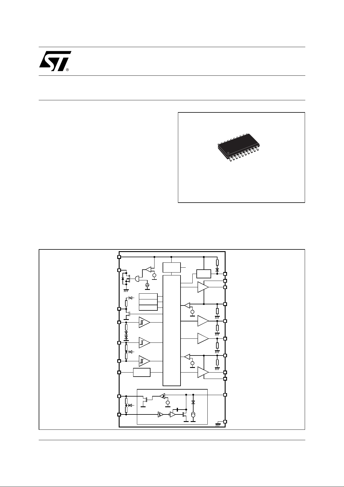
L9904
MOTOR BRIDGE CONTROLLER
PRODUCT PREVIEW
SO20
ORDERING NUMBER: L9904
DESCRIPTION
Control circuit for power MOS bridge driver in automotive applications with ISO 9141bus interface.
BLOCK DIAGRAM
PWM
DIR
10
VS
R
Reference
=
V
STH
f
ST
ISO-Interface
=
VCC
VCC
+
Overvolt age
Undervo ltage
Thermal shutdown
Timer
1
ST
R
DG
2
DG
4
EN
R
EN
5
R
DIR
R
PWM
3
6
PR
7
RX
R
RX
VCC
R
TX
8
TX
BIAS
0.5 • V
VCC
Charge
pump
=
V
S1TH
Control L ogi c
=
V
S2TH
VS
I
KH
CP
11
CP
13
CB1
12
GH1
14
S1
R
S1
19
GL1
R
GL1
18
GL2
R
GL2
17
S2
R
S2
15
GH2
16
CB2
9
K
20
GND
October 2002
This is preliminary information on a new product now in development. Details are subject to change without notice.
1/17
L9904
PIN FUNCTION
N° Pin Description
1 ST Open Drain Switch for Stepup converter
2 DG Open drain diagnostic output
3 PWM PWM input for H-bridge control
4 EN Enable input
5 DIR Direction select input for H-bridge control
6 PR Programmable cross conduction protection time
7 RX ISO 9141 interface, receiver output
8 TX ISO 9141 interface, transmitter input
9 K ISO 9141 Interface, bidirectional communication K-line
10 VS Supply voltage
11 CP Charge pump for driving a power MOS as reverse battery protection
12 GH1 Gate driver for power MOS highside switch in halfbridge 1
13 CB1 External bootstrap capacitor
14 S1 Source/drain of halfbridge 1
15 GH2 Gate driver for power MOS highside switch in halfbridge 2
16 CB2 External bootstrap capacitor
17 S2 Source/drain of halfbridge 2
18 GL2 Gate driver for power MOS lowside switch in halfbridge 2
19 GL1 Gate driver for power MOS lowside switch in halfbridge 1
20 GND Ground
PIN CONNECTION
2/17
(Top view)
ST
DG
PWM
EN
DIR
PR
RX
TX
K GH1
VS CP
2
3
4
5
6
7
8
9
10
SO20
20
19
18
17
16
15
14
13
12
11
GND1
GL1
GL2
S2
CB2
GH2
S1
CB1
ABSOLUTE MAXIMUM RATINGS
Symbol Parameter Value Unit
V
I
CB1
CB1
, V
, I
Bootstrap voltage -0.3 to 40 V
CB2
Bootstrap current -100 mA
CB2
L9904
V
I
CP
V
DIR
,V
PWM ,VTX
I
DIR
,I
PWM ,ITX
VDG ,V
CP
,V
,I
Charge pump voltage -0.3 to 40 V
Charge pump current -1 mA
Logic input voltage -0.3 to 7 V
EN
Logic input current ±1 mA
EN
Logic output voltage -0.3 to 7 V
RX
IDG ,IRX Logic output current -1 mA
V
GH1
I
GH1
V
GL1
I
GL1
V
VS1 , V
, V
, I
V
I
PR
, V
, I
PR
Gate driver voltage -0.3 to VSX + 10 V
GH2
Gate driver current -1 mA
GH2
Gate driver voltage -0.3 to 10 V
GL2
Gate driver current -10 mA
GL2
K-line voltage -20 to V
K
S
Programming input voltage -0.3 to 7 V
Programming input current -1 mA
Source/drain voltage -2 to VVS + 2 V
S2
V
I
S1
V
, I
V
ST
I
ST
VSDC
V
VSP
I
VS
Source/drain current -10 mA
S2
Output voltage -0.3 to 40 V
Step up output current -1 mA
DC supply voltage -0.3 to 28 V
Pulse supply voltage (T < 500ms) 40 V
DC supply current -100 mA
For externally applied voltages or currents exceeding these limits damage of the device may occur!
All pins of the IC are protected against ESD. The verification is performed according to MIL883C, human body
Ω
model with R=1.5k
, C=100pF and discharge voltage ±2kV, cor responding to a max imum dis charge ener gy of
0.2mJ.
3/17
L9904
THERMAL DATA
Symbol Parameter Value Unit
T
T
JSD
T
JSDH
R
th j-amb
1. see application note 110 for SO packa ges.
ELECT RICAL CH ARACTER ISTCS
Operating junction temperature -40 to 150 °C
J
Junction temperature thermal shutdown threshold min 150 °C
Junction thermal shutdown hysteresis typ 15 °C
Thermal resistance junction to ambient
1)
85 °C/W
(8V < VVS < 20V, VEN = HIG H, -40 °C ≤ TJ ≤ 150°C, unless otherwise spec-
ified. The voltages are refered to GND and currents are assumed positive, when current flows into the pin.
Symbol Parameter Test Condition Min. Typ. Max. Unit
Supply (VS)
V
VS OVH
Overvoltage disable HIGH
threshold
V
VS OVh
V
VS UVH
Overvoltage threshold hysteresis
Undervoltage disable HIGH
threshold
V
VS UVh
I
VSL
I
VSH
I
VSD
Undervoltage threshold
hysteresis
2)
Supply current VEN = 0 ; VVS = 13.5V; TJ< 85°C 50 µA
Supply current, pwm-mode VVS= 13.5V; VEN= HIGH;
Supply current, dc-mode VVS= 13.5V; VEN= HIGH;
Enable input (EN)
V
V
V
R
Low level 1.5 V
ENL
High level 3.5 V
ENH
ENh
Hysteresis threshold
Input pull down resistance VEN = 5V 16 50 100 kΩ
EN
2)
H-bridge control inputs (DIR, PWM)
V
V
PWML
V
DIRH
V
PWMH
V
V
PWMh
DIRL
DIRh
Input low level 1.5 V
Input high level 3.5 V
Input threshold hysteresis
2)
V
= LOW; S1 = S2 = GND
DIR
f
= 20kHz; C
PWM
= 4.7nF; C
C
GLX
R
= 10kΩ; C
PR
V
= LOW; S1 = S2 = GND
DIR
V
= LOW; C
PWM
= 10kΩ; C
R
PR
2)
CBX
GHX
= 150pF
PR
GHX
= 150pF
PR
= 0.1µF;
= 4.7nF;
= 4.7nF
28 33 36 V
1.6 V
67V
0.66 V
8.1 13 mA
5.8 10 mA
1V
1V
4/17
L9904
ELECTRICAL CHARACTERISTICS
(continued)
Symbol Parameter Test Condition Min. Typ. Max. Unit
R
R
PWM
Internal pull up resistance
DIR
to internal VCC
V
= 0; V
3)
DIR
= 0 16 50 100 kΩ
PWM
DIAGNOSTIC output (DG)
V
R
Programmable cross conduction protection
N
I
Output drop IDG = 1mA 0.6 V
DG
Internal pull up resistance
DG
to internal VCC
Threshold voltage ratio V
PR
V
PRL
Current capability
PR
3)
PRH
VDG = 0V 10 20 40 kΩ
4)
R
V
PR
PR
= 10kΩ
= 2V
1.8 2 2.2
-0.5 mA
/
ISO interface, transmission input (TX)
V
V
V
R
Input low level 1.5 V
TXL
Input high level 3.5 V
TXH
Input hysteresis voltage 2) 1 V
TXh
Internal pull up resistance to
TX
VTX = 0 10 20 40 kΩ
internal VCC 3)
ISO interface, receiver output (RX)
V
RXL
R
RX
R
RXON
t
RXH
t
RXL
Output voltage high stage
Internal pull up resistance
to internal VCC
3)
TX = HIGH; IRX = 0; V
TX = HIGH;
= 0V
V
RX
ON resistance to ground TX = LOW;
= 1mA
I
RX
Output high delay time Fig. 1 0.5 µs
Output low delay time 0.5 µs
= V
K
VS
4.5 5.5 V
51020kΩ
40 90 Ω
ISO interface, K-line (K)
R
V
V
V
I
I
KSC
Input low level -20V 0.45 ·
KL
Input high level
KH
Input hysteresis voltage 2) 0.025·
Kh
Input current VTX = HIGH -5 25 µA
KH
ON resistance to ground VTX = LOW; IK=10mA 10 30 Ω
KON
0.55 ·
V
VS
V
VS
Short circuit current VTX = LOW 40 130 mA
f
Transmission frequency 60 100 kHz
K
2. not tested in production: guaranteed by design and veri fied in charac terization
3. Internal V
4. see page 18 fo r calculation of programmable cross conduction protection time
is 4.5V ... 5.5V
VCC
V
VS
V
VS
0.8V
5/17
L9904
ELECTRICAL CHARACTERISTICS
(continued)
Symbol Parameter Test Condition Min. Typ. Max. Unit
t
Rise time VVS = 13.5V; Fig. 1
Kr
26µs
External loads at K-line:
= 510Ω pull up
R
K
to V
VS
C
= 2.2nF to GND
K
t
Fall time 26µs
Kf
t
t
t
Switch high delay time 4 17 µs
KH
Switch low delay time 4 17 µs
KL
Short circuit detection time VVS = 13.5V;
SH
10 40 µs
TX = LOW
> 0.55 · V
V
K
VS
Charge pump
V
I
t
Charge pump voltage VVS = 8V
CP
Charging current
CP
CP
= VVS + 8V
V
CP
Charging time
2)
VCP= VVS + 8V
= 13.5V
V
VS
= 20V
V
VS
V
= 13.5V -50 -75 µA
VS
V
= 13.5V
VS
C
= 10nF
CP
V
7V
V
10V
V
10V
VS
VS
VS
+
+
+
1.2 4 ms
VVS+
14V
V
VS
14V
V
VS
+14V
+
f
Charge pump frequency VVS = 13.5V 250 500 750 kHz
CP
Drivers for external highside power MOS
V
V
R
R
R
GH1H
R
GH2H
V
GH1H
V
GH2H
R
R
R
R
GH1L
GH2L
Bootstrap voltage VVS = 8V; I
CB1
CB2
ON-resistance of SINK stage
ON-resistance of SOURCE stage I
Gate ON voltage (SOURCE) VVS= VSX = 8V; I
Gate discharge resistance EN = LOW 10 100 kΩ
GH1
GH2
Sink resistance 10 100 kΩ
S1
S2
VVS =13.5V; I
VVS = 20V; I
V
CBX
I
GHX
V
CBX
I
GHX
GHX
I
GHX
C
CBX
V
= VSX = 13.5V; I
VS
C
CBX
V
= VSX = 20V; I
VS
C
CBX
CBX
CBX
CBX
= 8V; VSX = 0
= 50mA; T
= 8V; VSX = 0
= 50mA; T
= -50mA; TJ = 25°C
= -50mA; TJ = 125°C
= 0.1µF
= 0.1µF
= 0.1µF
= 0; VSX = 0
= 0; VSX = 0
= 0; VSX = 0
= 25°C
J
= 125°C
J
= 0;
GHX
= 0;
GHX
= 0;
GHX
7.5
10
10
V
VS
+6.5V
VVS+
10V
V
VS
+10V
14
14
14
10 Ω
20 Ω
10
20
V
VS
+14V
V
VS
+14V
V
VS
+14V
V
V
V
Ω
Ω
6/17
 Loading...