

1/17
L9903
June 2000
This ispreliminary information ona new product now in development. Details are subject to change without notice.
■
OPERATING SUPPLY VOLTAGE 8V TO 20V,
OVERVOLTAGE MAX. 40V
■
OPERATING SUPPLY VOLTAGE 6V WITH
IMPLEMENTED STEPUP CONVERTER
■ QUIESCENT CURRENT IN STANDBY MODE
LESS THAN 50µA
■
ISO 9141 COMPATIBLE INTERFACE
■
CHARGE PUMP FOR DRIVING A POWER
MOS AS REVERSE BATTERY PROTECTION
■ PWM OPERATION FREQUENCY UP TO
30KHZ
■ PROGRAMMABLE CROSS CONDUCTION
PROTECTION TIME
■
OVERVOLTAGE, UNDERVOLTAGE, SHORT
CIRCUIT AND THERMAL PROTECTION
■
REAL TIME DIAGNOSTIC
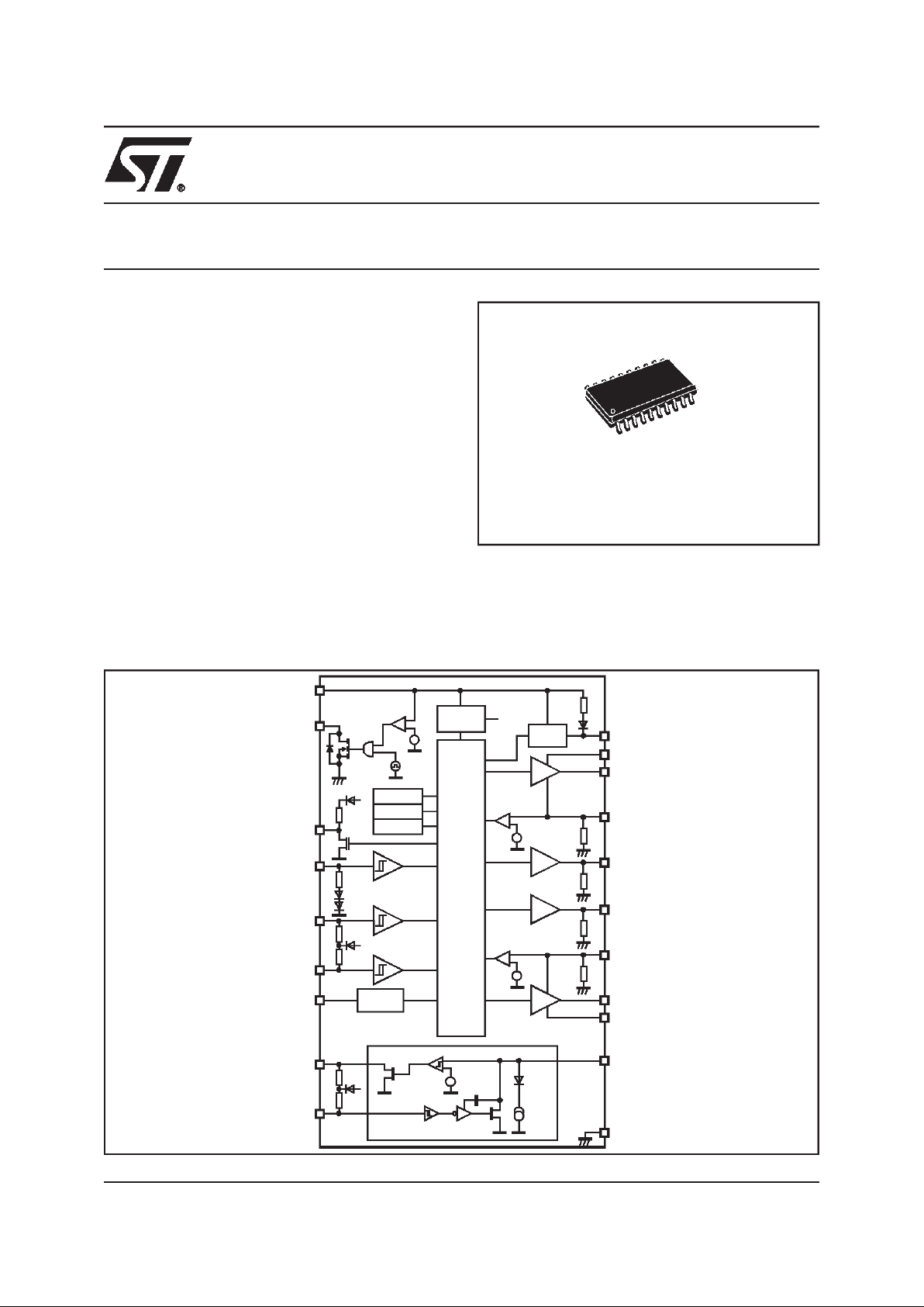
DESCRIPTION
Control circuit for power MOS bridge driver in automotive applications with ISO 9141bus interface.
SO20
ORDERING NUMBER: L9903
PRODUCT PREVIEW
MOTOR BRIDGE CONTROLLER
BLOCK DIAGRAM
VS
DIR
PWM
EN
RX
TX
CP
CB1
GH1
S1
GL1
CB2
GH2
S2
GL2
K
=
PR
VCC
=
=
ISO-Interface
VCC
GND
ST
Ref er enc e
BIAS
Char ge
pump
Control Logic
Overvoltage
Undervoltage
PWM
R
DIR
R
RX
R
TX
R
0.5 •V
VS
R
S2
R
GL2
R
GL1
R
S1
R
CP
R
EN
VCC
Timer
I
KH
V
S2TH
Thermalshutdown
V
S1TH
DG
VCC
R
DG
V
STH
f
ST
=
+
10
1
2
4
5
3
6
7
8
20
9
16
15
17
18
19
14
12
13
11
L9903
2/17
PIN FUNCTION
PIN CONNECTION (Top view)
N° Pin Description
1 ST Open Drain Switch for Stepup converter
2 DG Open drain diagnostic output
3 PWM PWM input for H-bridge control
4 EN Enable input
5 DIR Direction select input forH-bridge control
6 PR Programmable cross conduction protection time
7 RX ISO 9141 interface, receiver output
8 TX ISO 9141 interface, transmitter input
9 K ISO 9141 Interface,bidirectional communication K-line
10 VS Supply voltage
11 CP Charge pump for driving a power MOS as reverse battery protection
12 GH1 Gate driver for power MOS highside switch in halfbridge 1
13 CB1 External bootstrap capacitor
14 S1 Source/drain of halfbridge 1
15 GH2 Gate driver for power MOS highside switch in halfbridge 2
16 CB2 External bootstrap capacitor
17 S2 Source/drain of halfbridge 2
18 GL2 Gate driver for power MOS lowside switch in halfbridge 2
19 GL1 Gate driver for power MOS lowside switch in halfbridge 1
20 GND Ground
ST
DG
PWM
EN
DIR
RX
PR
TX
K GH1
CB1
S1
CB2
GH2
S2
GL2
GL1
GND1
3
2
4
5
6
7
8
9
18
17
16
15
14
12
13
11
19
10
20
VS CP
SO20
3/17
L9903
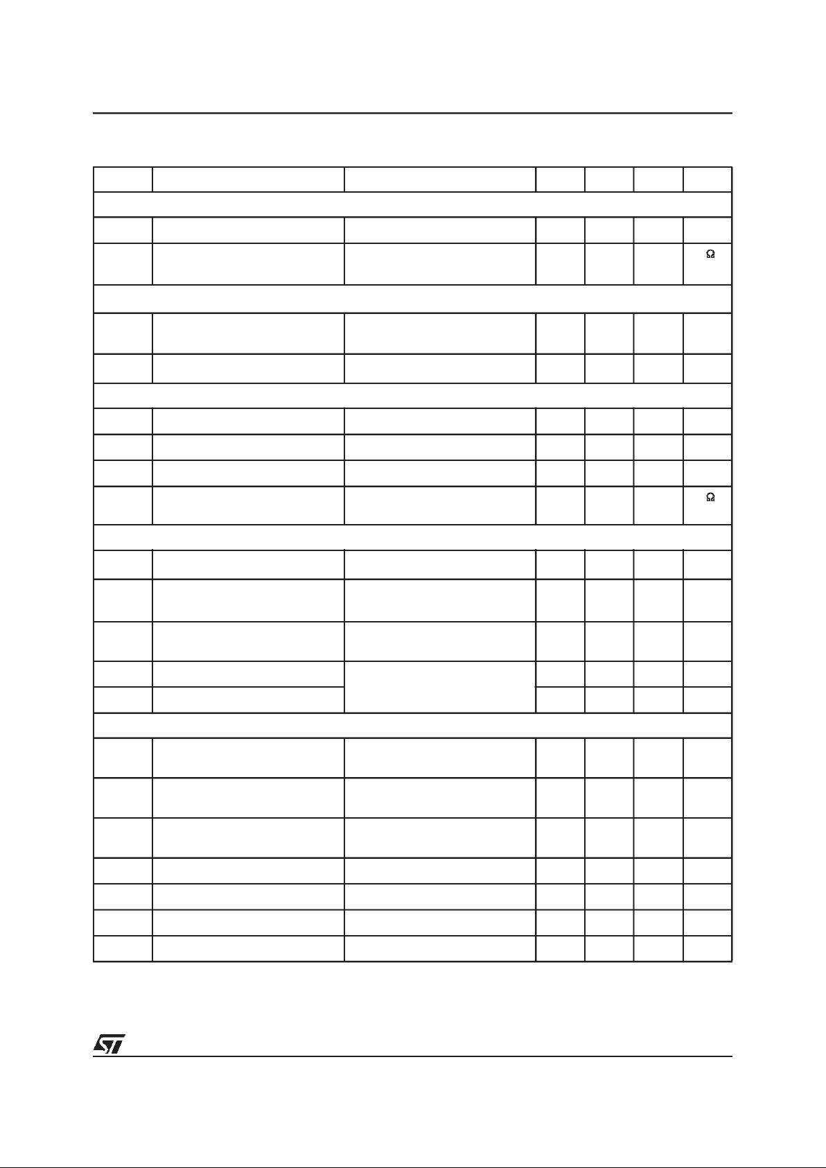
ABSOLUTEMAXIMUM RATINGS
For externally applied voltages or currents exceeding these limits damage of the device may occur!
All pins of the IC are protected against ESD. The verification is performed according to MIL883C, human body
model withR=1.5k
Ω, C=100pF and discharge voltage ±2kV, corresponding to a maximum discharge energy of
0.2mJ.
Symbol Parameter Value Unit
V
CB1,VCB2
Bootstrap voltage -0.3 to 40 V
I
CB1,ICB2
Bootstrap current -100 mA
V
CP
Charge pump voltage -0.3 to 40 V
I
CP
Charge pump current -1 mA
V
DIR,VEN
,V
PWM,VTX
Logic input voltage -0.3 to 7 V
I
DIR,IEN
,I
PWM,ITX
Logic input current ±1mA
V
DG,VRX
Logic output voltage -0.3 to 7 V
I
DG,IRX
Logic output current -1 mA
V
GH1,VGH2
Gate driver voltage -0.3 to VSX+10 V
I
GH1,IGH2
Gate driver current -1 mA
V
GL1,VGL2
Gate driver voltage -0.3 to 10 V
I
GL1,IGL2
Gate driver current -10 mA
V
K
K-line voltage -20 to V
S
V
V
PR
Programming input voltage -0.3 to 7 V
I
PR
Programming input current -1 mA
V
S1,VS2
Source/drain voltage -2 to VVS+2 V
I
S1,IS2
Source/drain current -10 mA
V
ST
Output voltage -0.3 to 40 V
I
ST
Step up output current -1 mA
V
VSDC
DC supply voltage -0.3 to 27 V
V
VSP
Pulse supply voltage (T £ 500ms) 40 V
I
VS
DC supply current -10 mA
L9903
4/17
THERMAL DATA
1. see application note 110 for SO packages.
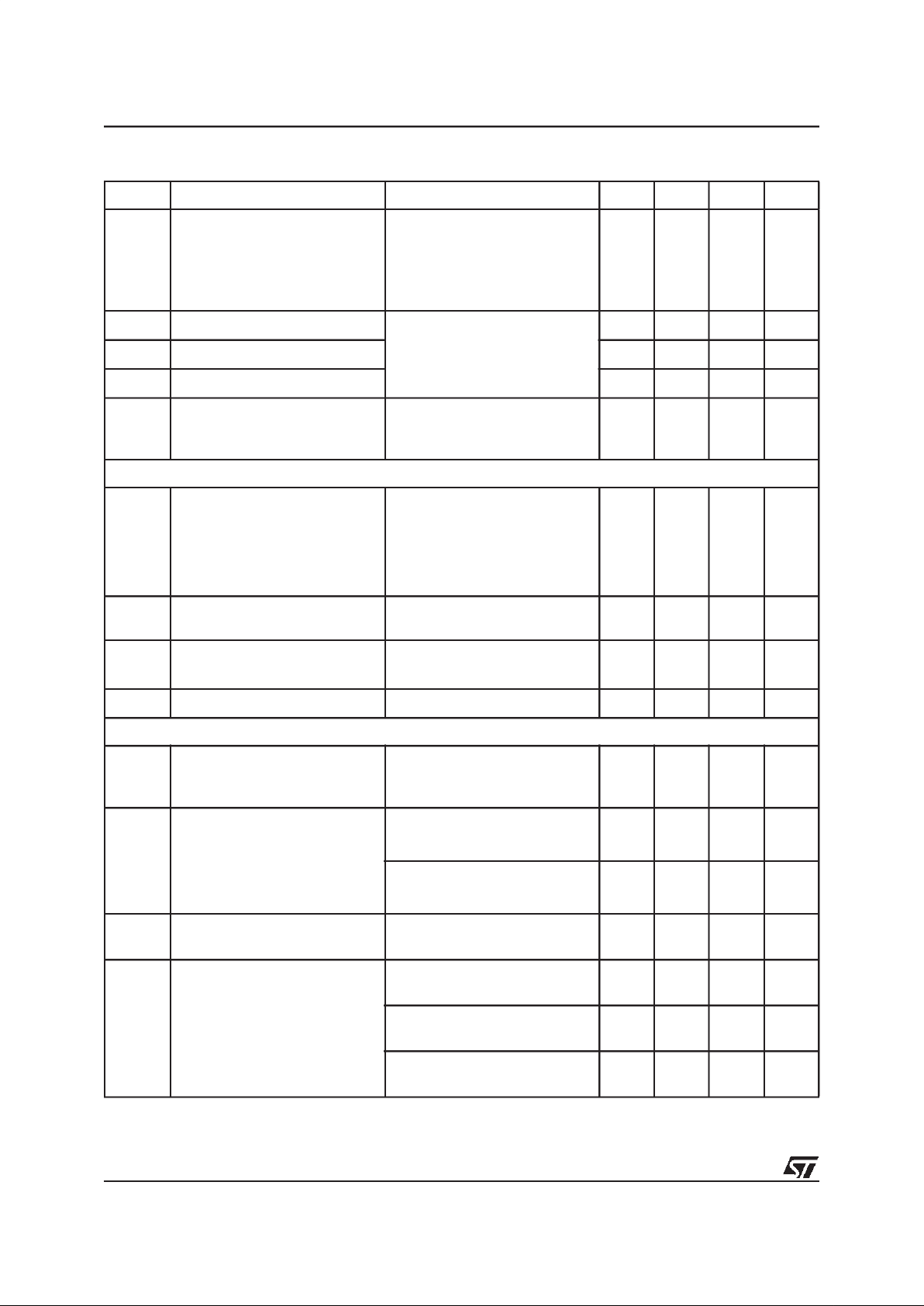
ELECTRICALCHARACTERISTCS (8V < V
VS
< 20V, VEN=HIGH, -40°C≤ T
J
≤ 150°C, unless otherwise spec-
ified. The voltages are refered to GND and currents are assumed positive, when current flows into the pin.
Symbol Parameter Value Unit
T
J
Operating junction temperature -40 to 150 °C
T
JSD
Junction temperature thermal shutdown threshold min 150 °C
T
JSDH
Junction thermal shutdown hysteresis typ 15 °C
R
th j-amb
Thermal resistance junction to ambient
1)
85 °C/W
Symbol Parameter Test Conditio n Min. Typ. Max. Unit
Supply (VS)
V
VS OVH
Overvoltage disable HIGH
threshold
20 22 24 V
V
VSOVh
Overvoltagethreshold hysteresis
2)
1.6 V
V
VS UVH
Undervoltage disable HIGH
threshold
67V
V
VS UVh
Undervoltage threshold
hysteresis
2)
0.66 V
I
VSL
Supply current VEN=0;VVS= 13.5V; TJ<85°C50µA
I
VSH
Supply current VVS= 13.5V; VEN= HIGH;
V
DIR
= LOW;
f
PWM
= 20kHz; C
CBX
= 0.1µF;
C
GLX
= 4.7nF; C
GHX
= 4.7nF;
R
PR
=10kΩ;CPR= 150pF
20 mA
Enable input (EN)
V
ENL
Low level 1.5 V
V
ENH
High level 3.5 V
V
ENh
Hysteresis threshold
2)
1V
R
EN
Input pull down resistance VEN=5V 16 50 100 kΩ
H-bridge control inputs (DIR, PWM)
V
DIRL
V
PWML
Input low level 1.5 V
V
DIRH
V
PWMH
Input high level 3.5 V
V
DIRh
V
PWMh
Input threshold hysteresis
2)
1V
R
DIR
R
PWM
Internal pull up resistance
to internal VCC
3)
V
DIR
=0;V
PWM
= 0 16 50 100 kΩ
5/17
L9903
DIAGNOSTIC output (DG)
V
DG
Output drop IDG= 1mA 0.6 V
R
DG
Internal pull up resistance
to internal VCC
3)
VDG=0V 10 20 40 kΩ
Programmable cross conduction protection
4)
N
PR
Threshold voltage ratio V
PRH
/
V
PRL
RPR= 10kΩ
1.8 2 2.2
I
PR
Current capability
V
PR
=2V
-0.5 mA
ISO interface, transmission input(TX)
V
TXL
Input low level 1.5 V
V
TXH
Input high level 3.5 V
V
TXh
Input hysteresis voltage 2) 1 V
R
TX
Internal pull up resistance to
internal VCC 3)
VTX= 0 10 20 40 kΩ
ISO interface, receiver output (RX)
V
RXL
Output voltage high stage
TX = HIGH; I
RX
=0;VK=V
VS
4.5 5.5 V
R
RX
Internal pull up resistance
to internal VCC
3)
TX = HIGH;
V
RX
=0V
51020k
Ω
R
RXON
ON resistance to ground TX = LOW;
I
RX
=1mA
40 90 W
t
RXH
Output high delay time Fig. 1 0.5 µs
t
RXL
Output low delay time 0.5 µs
ISO interface, K-line (K)
V
KL
Input low level -20V 0.45 ·
V
VS
V
KH
Input high level 0.55 ·
V
VS
V
VS
V
Kh
Input hysteresis voltage 2) 0.025·
V
VS
0.8V
I
KH
Input current VTX= HIGH -5 25 µA
R
KON
ON resistance to ground VTX= LOW; IK=10mA 10 30 W
I
KSC
Short circuit current VTX= LOW 40 130 mA
f
K
Transmission frequency 60 100 kHz
2. not tested in production: guaranteed by design and verified in characterization
3. Internal V
VCC
is 4.5V ... 5.5V
4. see page 18 for calculation of programmable cross conduction protection time
Symbol Parameter Test Conditio n Min. Typ. Max. Unit
ELECTRICAL CHARACTERISTICS
(continued)
L9903
6/17
t
Kr
Rise time VVS= 13.5V; Fig. 1
External loads at K-line:
R
K
=510Ωpull up
to V
VS
CK= 2.2nF to GND
26µs
t
Kf
Fall time 26µs
t
KH
Switch high delay time 4 17 µs
t
KL
Switch low delay time 4 17 µs
t
SH
Short circuit detection time VVS= 13.5V;
TX= LOW
V
K
> 0.55 · V
VS
10 40 µs
Charge pump
V
CP
Charge pump voltage VVS=8V
V
VS
= 13.5V
V
VS
= 20V
V
VS
+
7V
V
VS
+
10V
V
VS
+
10V
VVS+
14V
V
VS
+
14V
V
VS
+14V
I
CP
Charging current
V
CP=VVS
+8V
V
VS
= 13.5V -50 -75 µA
t
CP
Charging time
2)
VCP=VVS+8V
V
VS
= 13.5V
C
CP
= 10nF
1.2 4 ms
f
CP
Charge pump frequency VVS= 13.5V 250 500 750 kHz
Drivers for external highside powerMOS
V
CB1
V
CB2
Bootstrap voltage VVS= 8V; I
CBX
=0;VSX=0
V
VS
=13.5V; I
CBX
=0;VSX=0
V
VS
= 20V; I
CBX
=0;VSX=0
7.5
10
10
14
14
14
V
V
V
R
GH1L
R
GH2L
ON-resistance of SINK stage
V
CBX
= 8V; VSX=0
I
GHX
= 50mA; TJ=25°C
10 W
V
CBX
= 8V; VSX=0
I
GHX
= 50mA; TJ=125°C
20 W
R
GH1H
R
GH2H
ON-resistance of SOURCE stage I
GHX
= -50mA; TJ=25°C
I
GHX
= -50mA; TJ= 125°C
10
20
W
W
V
GH1H
V
GH2H
Gate ON voltage (SOURCE) VVS=VSX= 8V;I
GHX
=0;
C
CBX
= 0.1µF
V
VS
+6.5V
V
VS
+14V
V
VS=VSX
= 13.5V; I
GHX
=0;
C
CBX
= 0.1µF
V
VS
+
10V
V
VS
+14V
V
VS=VSX
= 20V; I
GHX
=0;
C
CBX
= 0.1µF
V
VS
+10V
V
VS
+14V
Symbol Parameter Test Conditio n Min. Typ. Max. Unit
ELECTRICAL CHARACTERISTICS
(continued)

7/17
L9903
R
GH1
R
GH2
Gate discharge resistance EN = LOW 10 100 kΩ
R
S1
R
S2
Sink resistance 10 100 kΩ
Drivers for external lowside power MOS
R
GL1L
R
GL2L
ON-resistance of SINK stage I
GLX
= 50mA; TJ=25°C
I
GLX
= 50mA; TJ= 125°C
10
20
W
W
R
GL1H,
R
GL2H
ON-resistance of SOURCE stage I
GLX
= -50mA; TJ=25°C
I
GLX
= -50mA; TJ= 125°C
10
20
W
W
V
GL1H,
V
GL2H
Gate ON voltage (SOURCE) VVS= 8V; I
GLX
=0
V
VS
= 13.5V; I
GLX
=0
V
VS
= 20V; I
GLX
=0
7V
10V
10V
V
VS
V
VS
14V
R
GL1
R
GL2
Gate discharge resistance EN = LOW 10 100 kΩ
2. not tested in production: guaranteed by design and verified in characterization
Timing of thedrivers
t
GH1LH
t
GH2LH
Propagation delay time Fig. 2
V
VS
= 13.5V
V
S1=VS2
=0
C
CBX
= 0.1µF
RPR= 10kW
500 ns
t
GH1LH
t
GH2LH
Propagation delay time including
cross conduction protection time
t
CCP
Fig. 2
V
VS
= 13.5V
V
S1=VS2
=0
C
CBX
= 0.1µF
C
PR
= 150pF;
R
PR
= 10kΩ;
5)
0.7 1 1.3 µs
t
GH1HL
t
GH2HL
Propagation delay time 500 ns
t
GL1LH
t
GL2LH
Propagation delay time Fig. 2
V
VS
= 13.5V
V
S1=VS2
=0
C
CBX
= 0.1µF
R
PR
= 10kΩ
500 ns
t
GL1LH
t
GL2LH
Propagation delay time including
cross conduction protection time
t
CCP
Fig. 2
V
VS
= 13.5V
V
S1=VS2
=0
C
CBX
= 0.1µF
C
PR
= 150pF;
R
PR
= 10kΩ;
5)
0.7 1 1.3 µs
t
GL1HL
t
GL2HL
Propagation delay time 500 ns
Symbol Parameter Test Conditio n Min. Typ. Max. Unit
ELECTRICAL CHARACTERISTICS
(continued)

L9903
8/17
t
GH1r
t
GH2r
Rise time Fig. 2
V
VS
= 13.5V
V
S1=VS2
=0
C
CBX
= 0.1µF
C
GHX
= 4.7nF
C
GLX
= 4.7nF
R
PR
= 10kΩ;
1 µs
t
GH1f
t
GH2f
Fall time 1 µs
t
GL1r
t
GL2r
Rise time 1 µs
t
GL1f
t
GL2f
Fall time 1 µs
Short Circuit Detection
V
S1TH
V
S2TH
Threshold voltage 4 V
t
SCd
Detection time 5 10 15 µs
Step up converter (ST) (5.2V≤ V
VS
< 10V)
V
STH
ST disable HIGHthreshold 10 V
V
STh
ST disable threshold hysteresis
voltage
2)
12V
R
DSON
Open drain ON resistance
V
VS
= 5.2V;
I
ST
=50mA
20
Ω
f
ST
Clock frequency 50 100 149 kHz
2. not tested in production: guaranteed by design and verifiedin characterization
5. tested with differed values in production but guaranteed by design and verified in characterization
Symbol Parameter Test Conditio n Min. Typ. Max. Unit
ELECTRICAL CHARACTERISTICS
(continued)

9/17
L9903
Figure 1. Timing of the ISO-interface
Figure 2. Timing of the drivers for the external MOS regarding the inputs DIR and PWM
t
TX
V
0.3 • V
VCC
0.7 • V
VCC
0.3 • V
VCC
t
V
K
t
t
KL
t
KH
t
Kr
t
Kf
IK>I
KSC
80%
20%
0.55 • V
VS
0.45 • V
VS
V
RX
t
RXL
t
RXH
0.3
• V
VCC
0.7 • V
VCC
ON
OFF
open drain
tra nsi s tor at
K-pin
t
SH
t
t
PWM
or
DIR
GHX
GLX
80%
20%
t
t
GHXHL
t
GHXf
t
GHXr
t
GHXLH
t
GLXHL
t
GLXLH
t
GLXf
t
GLXr
80%
20%

L9903
10/17
Figure 3. I(V) characteristics of the K-Line for TX = HIGH and VVS=13.5V
Figure 4. Driving sequence
-20 -10 0 10 20
VK[V]
-0.5
-0.4
-0.3
-0.2
-0.1
0.0
0.1
0.2
IK [mA]
~
50k
Ω
~
5
0k
Ω
EN
DIR
PWM
braking
GH1
GL1
GH2
GL2
Note:
Before standby mode
(EN = low) a braking phase
is mandatory to discharge
the stored energy of the
motor.

11/17
L9903
Figure 5. Charging time of an external capacitor of 10nF connected to CP pin at VVS=8V and
VVS=13.5V
Figure 6. Application Circuit Diagram
01234
time [ms]
0
5
10
15
20
25
30
voltage [V]
Charging time of a 10nF load at CP
CP for VS=13.5V
CP for VS=8V
EN
D1
µC
GND
K-Line
C1
R
R
R
R
Voltage
Regulator
V
BAT
C
S2
C
S1
R
PR
C
PR
C
B1
B2
C
V
CC
M
VS
DIR
PWM
EN
RX
TX
CP
CB1
GH1
S1
GL1
CB2
GH2
S2
GL2
K
=
PR
VCC
=
=
ISO-Interface
VCC
GND
ST
Reference
BIAS
Charge
pump
Control Logic
Overvoltage
Undervoltage
PWM
R
DIR
R
RX
R
TX
R
0.5 • V
VS
R
S2
R
GL2
R
GL1
R
S1
R
CP
R
EN
VCC
Timer
I
KH
V
S2TH
Thermals hutdown
V
S1TH
DG
VCC
R
DG
V
STH
f
ST
=
+
10
1
2
4
5
3
6
7
8
20
9
16
15
17
18
19
14
12
13
11
R
1
Gate
Protection

L9903
12/17
FUNCTIONAL DESCRIPTION
General
The L9903 integrated circuit (IC)is designed to control four external N-channel MOStransistors in H-Bridge configuration for DC-motordrivinginautomotive applications. It includes an ISO9141 compatible interface. A typical
application is shown in fig.6.
Voltagesupply
The IC is supplied via an external reverse battery protection diode tothe VVSpin. The typical operating voltage
range is down to 8V.
Extendedsupply voltage range (ST)
The operating battery voltage range can be extended down to 6V using the additional components shown in
fig.7. A small inductor of L~150µH(I
peak
~500mA) in series to the battery supply builts up a step up converter
with the switching open drain output ST. The switching frequency is typical 100kHz with a fixed duty cycle of
50%. The step up converter startsbelow V
VS
< 8V, increases the supply voltage at the VS pin and switches off
at V
VS
> 10V to avoid EME at nominal battery voltage. The diode D2 in series with the ST pin is necessary only
for systems with negative battery voltage. No additional load can be driven by the step up converter.
Figure 7.
V
BAT
L1 D1
D2
C1 C2
VS
ST
V
STH
f
ST
=
-
+
L9903

13/17
L9903
FUNCTIONAL DESCRIPTION
(continued)
Controlinputs(EN, DIR, PWM)
The cmos level inputs drive the device as shown in fig.4 and described in the truth table.
The device is activated with enable input HIGH signal. For enable input floating (not connected) or VEN=0V the
device is in standby mode.When activating the device a wake-up time of 50µs is recommended to stabilize the
internal supplies.
The DIR and PWM inputs control the driver of the external H-Bridge transistors. The motor direction can be
choosen with the DIR input, the duty cycle and frequency with the PWM input. Unconnected inputs are defined
by internal pull up resistors. During wake-up and braking and before disactivating the IC via enable both inputs
should be driven HIGH.
Truth table:
Symbols: x Don’t care R:Resistive output TS:Thermal shutdown
0: Logic LOW or not active L: Output in sink condition OV:Overvoltage
1: Logic HIGH or active H: Output in source condition UV:Undervoltage
T: Tristate SC:Short Circuit
6. Only those external MOS transistors of the H-Bridge which are in short circuit condition are switchedoff. Allothers remain driven
by DIR and PWM.
Thermalshutdown
When the junctiontemperature exceeds T
JSD
all driver are switched in sink condition (L), the K- output is off and
the diagnostic DG is LOW until the junction temperature drops below T
JSD-TJHYST
.
OvervoltageShutdown
When the supply voltage VVSexceeds the overvoltage threshold V
VSOVH
all driver are switched in sink condi-
tion (L), the K- output is off and the diagnostic DG is LOW.
Status Controlinputs Device status
Driver stage for external
power MOS
Diagnostic Comment
EN DIR
PWM TS OV UV SC GH1 GL1 GH2 GL2 DG
1 0xxxxxxRRRR T standby mode
2 1xx1000LLLL L thermal
shutdown
3 1xx0100LLLL L overvoltage
4 1xx0010LLLL L undervoltage
5 1xx0001
X
6)
X
6)
X
6)
X
6
L
short circuit
6)
6 1000000LHHL H
7 1x10000HLHL H braking mode
8 1100000HLLH H

L9903
14/17
FUNCTIONAL DESCRIPTION
(continued)
Undervoltage Shutdown
For supply voltages below the undervoltage disable threshold the gate driver remains in sink condition (L) and
the diagnostic DG is low.
Short CircuitDetection
The output voltage at the S1 and S2 pin of the H-Bridge is monitoredbycomparators to detect shorts to ground
or battery. The activated external highside MOS transistor will be switched offifthe voltage drop remains below
the comparator threshold voltage V
S1TH
and V
S2TH
for longer than the short current detection time t
SCd
. The
transistor remains in off condition, the diagnostic output goes LOW until the DIR or PWM input status will be
changed. The status doesn’t change for the other MOS transistors. The external lowside MOS transistor will be
switched off if the voltage drop passes over the comparator threshold voltage V
S1TH
and V
S2TH
for longer than
the short current detection time t
SCd
. The transistor remains in off condition, the diagnostic output goes LOW
until the DIR or PWM input status will be changed. The status doesn’t change for the other MOS transistors.
Diagnostic Output (DG)
The diagnostic output provides a realtime error detection, if monitors the following error stacks: Thermal shutdown, overvoltage shutdown , undervoltage shutdown and short circuit shutdown. The open drain output with
internal pull up resistor is LOW if an error is occuring.
Bootstrapcapacitor (CB1,CB2)
To ensure, that the external power MOS transistors reach the required R
DSON
, a minimum gate source voltage
of 5V for logic level and 10V for standard power MOS transistors has tobeguaranteed. The highside transistors
require a gate voltage higher than the supply voltage. This is achieved with the internal chargepump circuit in
combination withthe bootstrap capacitor. The bootstrap capacitor ischarged, when the highside MOStransistor
is OFF and the lowside is ON. When the lowside is switched OFF, the charged bootstrap capacitor is able to
supply the gate driver of the highside power MOS transistor. For effective charging the values of the bootstrap
capacitors should be largerthan the gate-source capacitance of the power MOS and respect the required PWM
ratio.
Chargepump circuit (CP)
The reversebattery protection can be obtained with an external N-channel MOS transistor as shown infig.6. In
this case its drain-bulk diode provides the protection. The output CP is intended to drive the gate of this transistor above the battery voltage to switch on the MOS and to bypass the drain-bulk diode with the R
DSON
.The
CP has a connection to VS through an internal diode and a 20k
Ω resistor.
Gate drivers for the external N-channel power MOS transistors(GH1, GH2, GL1, GL2)
High level at EN activates the driver of the external MOS under control of the DIR and PWM inputs (see truth
table and driving sequence fig.4). The external power MOS gates are connected via series resistors to the device to reduce electro magnetic emission (EME) of the system. The resistors influence the switching behaviour.
They have to be choosen carefully. Too large resistors enlarge the charging and discharging time of the power
MOS gate and can generate cross current in the halfbridges. The driver assures a longer switching delay time
from source to sink stage in order to prevent the cross conduction.
The gate source voltage is limited to 14V. The charge/discharge current is limited by the R
DSON
of the driver.
The drivers are not protected against shorts.

15/17
L9903
FUNCTIONAL DESCRIPTION (continued)
Programmablecross conductionprotection
The external power MOS transistors in H-Bridge ( two half bridges) configuration are switched on with an additional delay time t
CCP
to prevent cross conduction in the halfbridge. The cross conduction protection time
t
CCP
isdetermined by the external capacitorCPRandresistor RPRat the PR pin. The capacitor CPRis charged
up to the voltage limitV
PRH
. A level change on the control inputs DIR and PWM switches off the concerned ex-
ternal MOS transistor and the charging source at the PR pin. The resistor R
PR
discharges the capacitor CPR.
The concerned external power MOS transistor will be switched on again when the voltage at PR reaches the
value of V
PRL
. After that the CPR will be charged again. The capacitor CPRshould be choosen between 100pF
and 1nF. The resistor R
PR
should be higher than 7kW. The delay time can be expressed as follows:
t
CCP=RPR·CPR
·lnN
PR
with NPR=V
PRH/VPRL
=2
t
CCP
= 0.69 · RPR·C
PR
ISO-Interface
The ISO-Interface provides the communication between the micro controller and a serial bus with a baud rate
up to 60kbit/s viaa single wire whichis V
BAT
and GND compatible. The logic level transmission input TX drives
the open drain K-output. The K output can be connected to a serial bus with a pull up resistor to V
BAT
. The K-
pin is protected against overvoltage, short to GND and VS and can be driven beyond V
VS
and GND. During lack
of V
VS
or GND the output shows high impedance characteristic. Theopen drain output RX with an internal pull
up resistor monitors the status at the K-pin to read the received data and control the transmitted data. Short
circuit condition at K-pin is recognized if the internal open drain transistor isn’t able to pull the voltage potential
at K-pin below the threshold of 0.45·VVS. Then the RX stays in high condition. A timer starts and switches the
open drain transistor after typ. 20µs off. A next low at the TX input resets the timerand the open drain transistor
switches on again.
Figure 8. Functional schematic of the ISO-interface
RX
TX
K
V
CC
R
RX
0.5
•V
VS
TX
R
T
SH
delay
=
R
S
Q
R
I
KH

L9903
16/17
110
1120
A
e
B
D
E
L
K
H
A1
C
SO20MEC
hx45°
SO20
DIM.
mm inch
MIN. TYP. MAX. MIN. TYP. MAX.
A 2.35 2.65 0.093 0.104
A1 0.1 0.3 0.004 0.012
B 0.33 0.51 0.013 0.020
C 0.23 0.32 0.009
0.013
D 12.6 13 0.496 0.512
E 7.4 7.6 0.291 0.299
e 1.27 0.050
H 10 10.65 0.394 0.419
h 0.25 0.75 0.010 0.030
L 0.4 1.27 0.016 0.050
K0°(min.)8°(max.)
OUTLINE AND
MECHANICAL DATA

Information furnished isbelieved to be accurate and reliable. However, STMicroelectronics assumes no responsibility for the consequences
of useof suchinformation nor for any infringement of patents or otherrightsofthird parties whichmay result from its use.No license is granted
by implicationor otherwise under any patent or patent rights of STMicroelectronics. Specifications mentioned in this publication are subject
to change without notice. This publication supersedes and replaces all information previously supplied. STMicroelectronics products are not
authorized for use as critical components in life support devices or systems without express written approval of STMicroelectronics.
The ST logo is a registered trademark of STMicroelectronics
2000 STMicroelectronics - All Rights Reserved
STMicroelectronics GROUP OF COMPANIES
Australia - Brazil - China - Finland - France - Germany - Hong Kong - India- Italy - Japan - Malaysia -Malta- Morocco - Singapore - Spain
- Sweden - Switzerland - United Kingdom - U.S.A.
http://www.st.com
17/17
L9903
 Loading...