

L98SI
OCTALSERIAL SOLENOID DRIVER
.EIGHTLOWR
(0.5ΩATI
=1A@25°CVCC=5V±5%)
O
DMOSOUTPUTS
DSon
.8 BITSERIAL INPUT DATA (SPI)
.
8 BIT SERIAL DIAGNOSTIC OUTPUT FOR
OVERLOADANDOPENCIRCUITCONDITIONS
.OUTPUT SHORT CIRCUITPROTECTION
.CHIPENABLESELECTFUNCTION(activelow)
.INTERNAL 36V CLAMPINGFOR EACH OUT-
PUT
.CASCADABLE WITH ANOTHER OCTAL
DRIVER
.LOWQUIESCENTCURRENT (10mAMAX.)
.
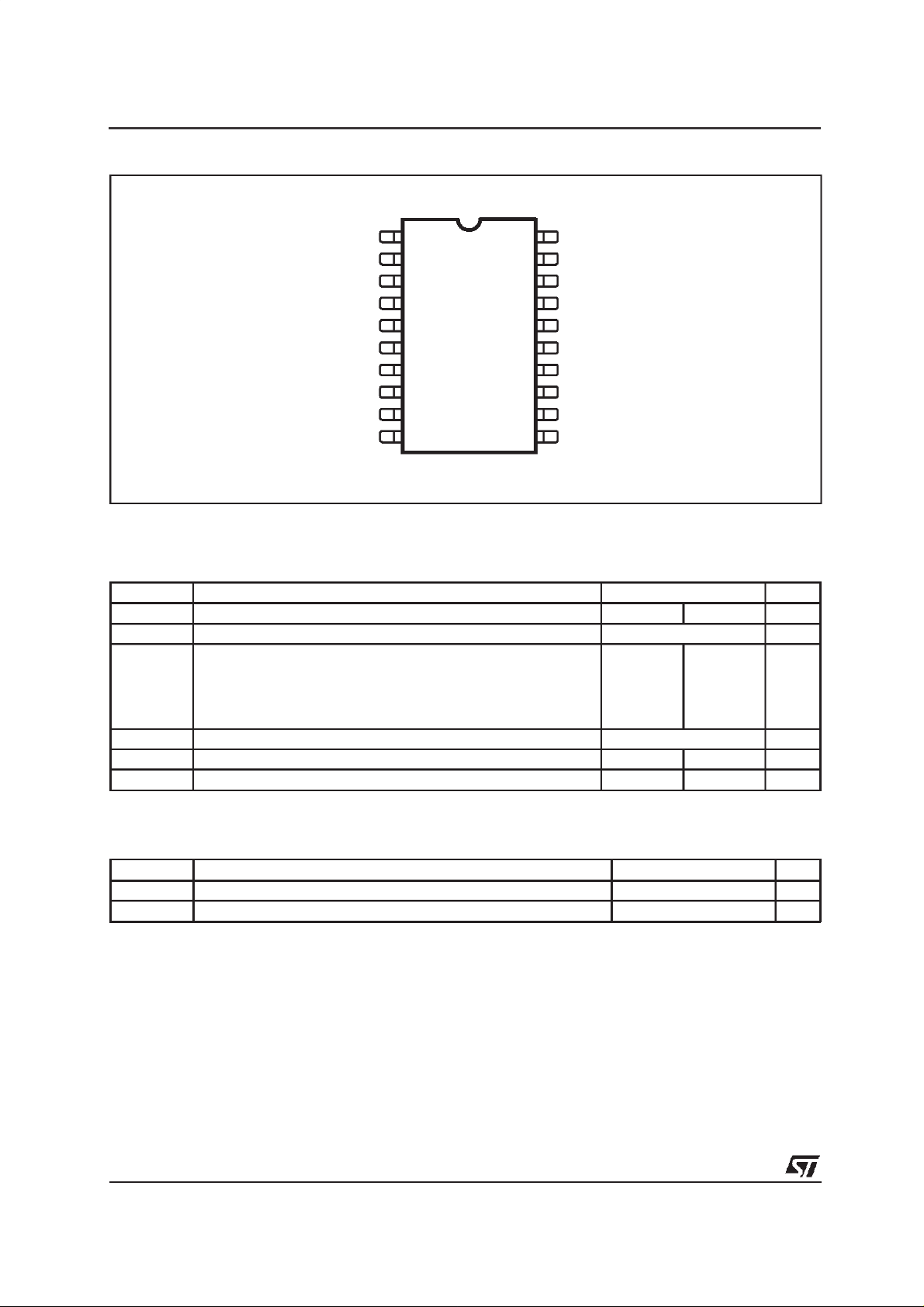
PACKAGE PowerSO20
DESCRIPTION
TheL98SI is anoctal low side solenoiddriverrea
lizedin Multipower-BCDtechnologyparticularlysuited for drivinglamps,relays and solenoidsin indu-
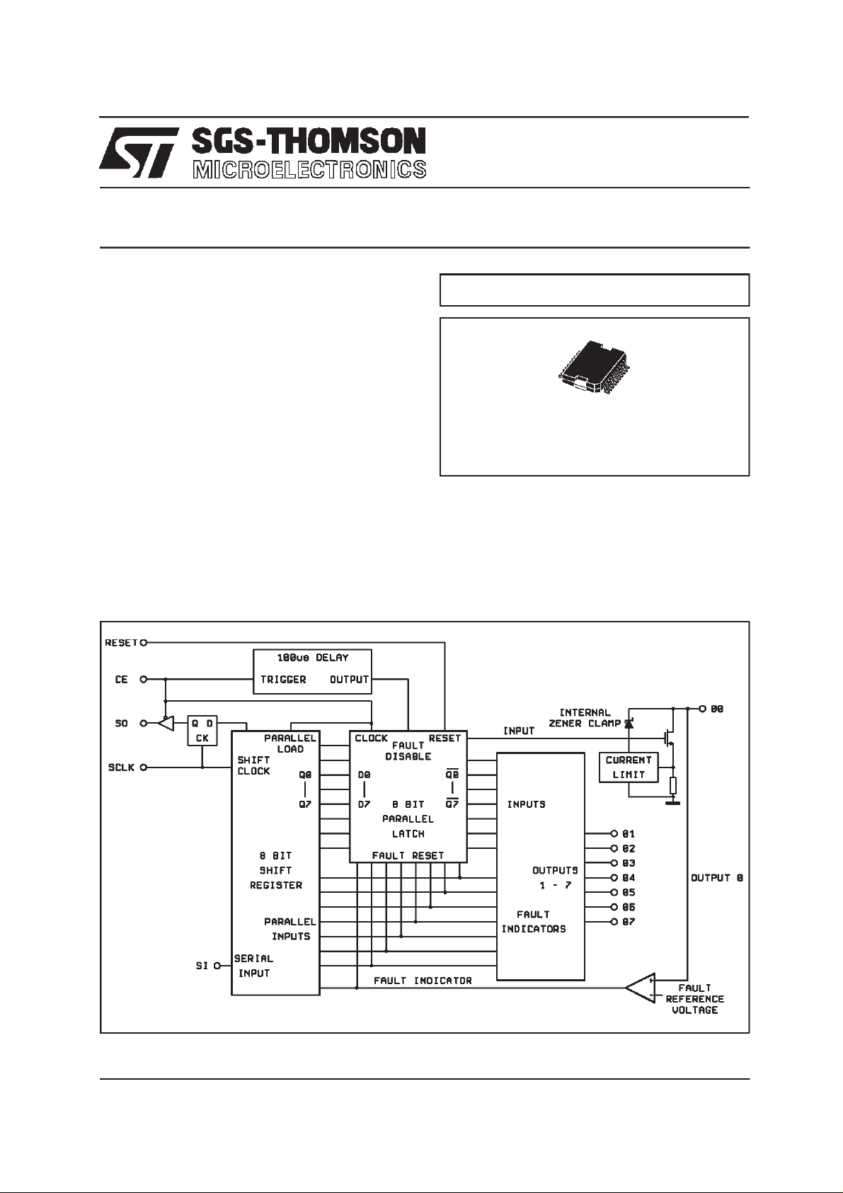
BLOCKDIAGRAM
MULTIPO WER BCD TECHNOLOG Y
PowerSO20
ORDERING NUMBER: L98SI
strial environment.The L98SIDMOSoutputshave
verylow power consumption.
Data is transmitted serially to the device usingthe
SerialPeripheralInterface(SPI) protocol.
The L98SI features the outputs status monitoring
function.
April 1998
1/9
L98SI
PIN CONNECTION(topview)
GND
SO
V
DD
RESET
OUT7
OUT6
OUT5
OUT4
N.C. N.C.
GND GND
2
3
4
5
6
7
8
9
10
D94AT119
20
19
18
17
16
15
14
13
12
11
GND1
SI
SCLK
CE
OUT0
OUT1
OUT2
OUT3
ABSOLUTEMAXIMUM RATINGS
Symbol Parameter Value Unit
DC Logic Supply – 0.7 7 V
Output Voltage internally clamped V
Input Transient Current
(CE, SI, SCLK, RESET, SO) :
Duration Time t = 1s,
VI<0
V
I>VCC
–25
Continuous Output Current (for each output) Int. Limited A
Junction and Storage Temperature Range – 40 150
stg
Max Clamping Energy (for each output) 200 mJ
+25
T
j
V
DD
V
O
I
I
I
Odc
,T
E
X
mA
mA
°
C
THERMAL DATA
Symbol Parameter Value Unit
Thermal Resistance Junction-Case Max. 1.5
Thermal Resistance Junction-Ambient Max. 60
2/9
R
th j-case
R
th j-amb
C/W
°
C/W
°
PIN DESCRIPTION
L98SI
V
CC
Logicsupplyvoltage - nominally 5V
GROUND
DeviceGround.Thisgroundappliesforthelogiccircuitsas well as the poweroutputstages.
RESET
Asynchronousresetfortheoutputstages,theparal-
lellatchand theshiftregisterinsidethe L98SI.This
pinisactivelowandit mustnot beleftfloating.Apoweron clearfunctionmaybe implementedconnecting this pin to V
with an external resistor and to
CC
groundwith an externalcapacitor.
CE
ChipEnable. Datais transferredfromthe shift registerstotheoutputson the risingedgeof thissignal.
Thefalling edgeof this signalsets the shiftregister
with the outputvoltagesensebits coming from the
output stages.The output driver for the SO pin is
enabledwhen this pinis low.
SO
SerialOutput.This pin is theserial outputfrom the
shift register and it is tri-stated when CE is high.A
highfor a data bit on this pin indicatesthat the par-
ticularoutput is high. A low on thispin for adata bit
indicatesthat the outputis low.
Comparing the serial output bits with the previous
serial input bits the external microcontroller implementsthediagnosticdata suppliedby theL98SI.
SI
SerialInput.Thispin is theserialdata input.A high
onthispinwillprogramaparticularoutputtobeOFF,
whilea lowwill turn itON.
SCLK
SerialClock.This pin clocksthe shift register.New
SO data will appearon every rising edgeof thispin
andnewSIdatawillbe latchedoneverySCLK’sfallingedgeinto theshiftregister.
OUTPUTS00-07
Poweroutputpins.The inputandoutputbitscorres-
pondingto07 aresentandreceivedfirstviatheSPI
busand 00is thelast.Theoutputsareprovidedwith
currentlimiting andvoltagesensefunctionsfor fault
indicationand protection.The nominal load current
for theseoutputsis 500mA,but the current limiting
issetto a minimumof1.05A.Theoutputsalsohave
on board clamps set at about 36V for recirculation
of inductiveloadcurrent.
ELECTRICALCHARACTERISTICS (V
Symbol Parameter Test Conditions Min. Typ. Max. Unit
Output Clamping Volt. IO= 0.5A, Output Programmed OFF 30 40 V
Out. Leakage Current VO= 24V, Output Progr. OFF 1 mA
On Resistance Output Progr. ON
Out. Self Limiting
Current
Turn-on Delay IO= 500mA
Turn-off Delay IO= 500mA
Fault Refer. Voltage Output Progr. OFF
Fault Reset Delay
(after CE L to H
transition)
Output OFF Voltage Output Pin Floating.cOutput Progr. OFF, 1.0 V
I
R
V
V
V
OC
Oleak
DSon
I
OL
t
PHL
t
P
OREF
t
UD
OFF
=5V±5%.Tj=– 40to 125°C ; unlessotherwise speciifed)
CC
I
= 0.5A
O
= 0.8A
I
O
I
=1A
O
With Fault Reset Disabled
Output Progr. ON 1.05 A
No Reactive Load
No Reactive Load
1.6 2 V
Fault detected if V
See fig. 3 75 250 µs
O>VOREF
0.55
0.55
0.55
1
1
1
10
10
Ω
Ω
Ω
s
µ
s
µ
3/9

L98SI
ELECTRICALCHARACTERISTICS (Continued)
Symbol Parameter Test Conditions Min. Typ. Max. Unit
INPUTBUFFER(SI, CE, SCLK andRESETpins)
V
T–
Threshold Voltage at
VCC=5V±10% 0.2V
Falling Edge
SCLK only
V
T+
Threshold Voltage at
VCC=5V±10% 0.7V
Rising Edge
SCLK only
V
C
H
I
I
Hysteresis Voltage VT+–V
T–
Input Current VCC= 5.50V, 0 < VI<V
Input Capacitance 0 < VI<V
I
CC
CC
OUTPUT BUFFER(SO pin)
V
SOL
V
SOH
I
SOtl
C
SO
I
CC
Output LOW Voltage IO= 1.6mA 0.4 V
Output HIGH Voltage IO= 0.8mA V
Output Tristate Leakage
Current
Output Capacitance 0 < VO<V
0<VO<VCC, CE Pin Held High,
= 5.25V
V
CC
CC
CE Pin Held High
Quiescent Supply
Current at V
CC
Pin
All Outputs Progr. ON. I
O
per Output Simultaneously
= 0.5A
SERIALPERIPHERAL INTERFACE (see fig.2, timingdiagram)
f
op
t
lead
t
lag
t
wSCKH
t
wSCKL
t
su
t
H
t
EN
t
DIS
t
t
rSO
t
fSO
t
rSI
t
fSI
t
ho
V
Operating Frequency D.C. 2 MHz
Enable Lead Time 250 ns
Enable Lag Time 250 ns
Clock HIGH Time 200 ns
Clock LOW Time 200 ns
Data Setup Time 75 ns
Data Hold Time 75 ns
Enable Time 250 ns
Disable Time 250 ns
Data Valid Time 100 ns
Rise Time (SO output) VCC= 20 to 70% CL= 200pF 50 ns
Fall Time (SO output) VCC= 70 to 20% CL= 200pF 50 ns
Rise Time SPI
VCC= 20 to 70% CL= 200pF 200 ns
Inputs (SCK, SI, CE)
Fall Time SPI
VCC= 70 to 20% CL= 200pF 200 ns
Inputs (SCLK, SI, CE)
Output Data Hold Time 0
CC
0.6
CC
4.15
0.85 2.5 V
–10 +10
20 nF
CC
– 1.3V
–20 20
20 pF
10 mA
µ
µ
V
V
V
V
A
V
A
s
µ
4/9

FUNCTIONALDESCRIPTION
TheL98SIDMOSoutputisalowoperatingpowerdevicefeatu-ring,eight 1Ω R
DMOSdrivers with
DSON
transient protection circuits in output stages. Each
channel is independently controlled by an output
latchanda commonRESET line which disablesall
eightoutputs.Thedriverhaslowsaturationandshort
circuitprotectionandcandriveinductiveandresistive
loads such as solenoids, lamps and relais. Data is
transmittedtothedeviceseriallyusingtheSerialPeripheralInterface(SPI)protocol.Thecircuitreceives
8bitserialdatabymeansoftheserialinput(SI)which
is storedin an internalregisterto control the output
drivers.The serialoutput(SO) provides 8 bit of diagnosticdatarepresentingthevoltagelevelatthedriver output. This allows the microprocessor to
diagnosetheconditionofthe outputdrivers.
The output saturation voltage is monitored by a
comparatorfor an outof saturationconditionandis
abletounlatchtheparticulardriverthroughthefault
resetline. This circuitis also cascadablewith another octal driver in order to jam 8 bit multiple data.
The device is selected when the chip enable (CE)
lineis low.
Additionallythe (SO) is placed in a tri-state mode
when the deviceis deselected.The negativeedge
of the(CE) transfersthe voltagelevelof thedrivers
tothe shiftregisterand thepositiveedgeofthe(CE)
latchesthenewdatafromtheshiftregistertothedrivers. WhenCE is Low, data bit containedinto the
shift register is transferred to SO output at every
SCLKpositivetransitionwhiledatabit presentatSI
inputis latchedintotheshiftregisteroneverySCLK
negativetransition.
InternalBlocks Description
The internalarchitectureof the deviceis basedon
the threeinternalmajorblocks: the octalshiftregisterfortalkingto the SPIbus,the octallatchfor holdingcontrolbits writtenintothe deviceandthe octal
load driverarray.
Shift Register
The shiftregisterhas bothserialandparallelinputs
and serial and parallel outputs.Theserial input acceptsdatafromthe SPIbusandtheserialoutputsimultaneously sends data into the SPI bus. The
paralleloutputsarelatchedintotheparallellatchinsidethe L98SIatthe endof a datatransfer.Theparallelinputsjam diagnosticdataintotheshiftregister
at thebeginningof a data transfercycle.
ParallelLatch
The parallellatchholdstheinputdatafromthe shift
register.This data then actuatestheoutputstages.
L98SI
Individualregisters in the latch may be clearedby
fault conditions in order to protectthe overloaded
outputstages.The entire latchmay also becleared
by theRESET signal.
OutputStages
Theoutputstagesprovidean activelowdrivesignal
suitable for 0.75A continuous loads. Each output
has a currentlimit circuit whichlimitsthe maximum
outputcurrentto at least1.05A to allow for highinrushcurrents.Additionally,theoutputshaveinternal
zenersset to 36 voltsto clampinductivetransients
at turn-off.Each outputalso has a voltagecomparatorobservingtheoutputnode.If thevoltageexceeds 1.8V on an ON output pin, a fault condition is
assumedand the latch drivingthis particular stage
is reset, turningthe outputOFF toprotectit. Thetiming of thisactionis describedbelow.These comparators also provide diagnostic feedback data to
theshiftregister.Additionally,thecomparatorscontainaninternalpulldowncurrentwhichwillcausethe
cell to indicate a low outputvoltage if the output is
programmedOFF and the outputpinisopencircuited.
TIMINGDATA TRANSFER
Figure#2 showsthe overall timing diagramfrom a
byte transferto and from the L98SI using the SPI
bus.
CE Highto LowTransition
Theactionbegins whenthe ChipEnable(CE)pinis
pulledlow.Thetri-stateSerialOutput(SO)pin driver
willbeenabledentire timethatCE islow.Atthefallingedge of theCEpin,thediagnosticdata fromthe
voltagecomparatorsin theoutputstageswillbelatched into the shift register. If a particularoutput is
high, a logic one will be jammedinto that bit in the
shiftregister.Iftheoutputis low,a logiczerowillbe
loadedthere.Themostsignificantbit(07)shouldbe
presentedat theSerial Input(SI) pin.A zero at this
pin will programan outputON,whilea one will programthe outputOFF.
SCLK Transitions
The Serial Clock(SCLK) pin shouldthenbe pulled
high.Atthispointthediagnosticbit fromthemostsignificantoutput(07)willappearattheSOpin.Ahigh
here indicates that the 07 pin is higher than 1.8V.
TheSCLKpinshouldthenbe toggledlowthenhigh.
NewSOdatawillappearfollowingeveryrisingedge
of SCLK and new SI data will be latched into the
L98SIshiftregisteronthefallingedges.Anunlimited
amount of data may be shiftedthrough the device
5/9

L98SI
shiftregister(intotheSI pinandout the SO pin), allowingtheotherSPIdevicesto becascadedinadaisychain with the L98SI.
CELow to HighTransition
Once the last data bit has been shifted into the
L98SI,the CE pin should be pulledhigh.
Attherisingedgeof CE the shiftregisterdataislatchedintotheparallellatchandtheoutputstageswill
beactuatedbythe newdata.An internal160µsdelaytimerwillalso be startedat thisrisingedge (see
). During the 160µs period, the outputs will be
t
UD
protectedonlyby theanalogcurrentlimiting circuits
since the resettingof the parallel latches by faults
conditionswillbeinhibitedduringthisperiod.Thisallowsthe part toovercomeany highinrushcurrents
that may flow immediately after turn on. Once the
delay period has elapsed, the output voltages are
sensedbythe comparatorsand anyoutputwithvoltageshigherthan1.8VarelatchedOFF.Itshouldbe
notedthat the SCLK pin shouldbe low at both tran-
Figure 1
: Byte Timing with AsynchronousReset.
sitionsof the CE pin to avoid any false clocking of
theshiftregister.TheSCLKinputisgatedbytheCE
pin, so that the SCLK pin is ignored wheneverthe
CE pinis high.
FAULTCONDITIONSCHECK
Checkingforfaultconditionsmaybe donein thefol-
lowing way. Clock in a new control byte. Wait 160
microseconds or so to allow the outputs to settle.
Clockinthesamecontrolbyteandobservethediagnosticdata that comes outof the device.The diagnostic bits should be identical to the bits that were
firstclockedin. Anydifferenceswouldpointtoa fault
onthatoutput.IftheoutputwasprogrammedONby
clockingina zero,anda one camebackas the diagnosticbitforthatoutput,theoutputpinwasstillhigh
anda shortcircuit oroverloadconditionexists.Ifthe
output was programmedOFF by clocking in a one,
and a zerocameback asthe diagnosticbit for that
output,nothinghad pulledtheoutputpin highandit
6/9

Figure 2 : Timing Diagram.
L98SI
Figure 3
: TypicalApplicationCircuit.
7/9

L98SI
POWERSO20 PACKAGE MECHANICAL DATA
DIM.
MIN. TYP. MAX. MIN. TYP. MAX.
mm inch
A 3.6 0.142
a1 0.1 0.3 0.004 0.012
a2 3.3 0.130
a3 0 0.1 0.000 0.004
b 0.4 0.53 0.016 0.021
c 0.23 0.32 0.009 0.013
D (1) 15.8 16 0.622 0.630
D1 9.4 9.8 0.370 0.386
E 13.9 14.5 0.547 0.570
e 1.27 0.050
e3 11.43 0.450
E1 (1) 10.9 11.1 0.429 0.437
E2 2.9 0.114
E3 5.8 6.2 0.228 0.244
G 0 0.1 0.000 0.004
H 15.5 15.9 0.610 0.626
L 0.8 1.1 0.031 0.043
N10°(max.)
S8°(max)
T 10 0.394
(1) ”D and F” do not include mold flash or protrusions.
- Mold flash or protrusions shall not exceed 0.15 mm (0.006”).
- Critical dimensions: ”E”, ”G” and ”a3”
NN
a2
e
1120
E1
E2
b
DETAILA
110
e3
D
T
A
DETAIL B
R
a3
Gage Plane
lead
E
DETAILB
0.35
S
L
c
a1
DETAILA
slug
-C-
SEATING PLANE
GC
(COPLANARITY)
8/9
hx45°
PSO20MEC

L98SI
Information furnished is believed to be accurate and reliable. However, SGS-THOMSON Microelectronics assumes no responsibility for
the consequences of use of such information nor for any infringement of patents or other rights of third parties which may result from its
use. No license is granted by implication or otherwise under any patent or patent rights of SGS-THOMSON Microelectronics. Specification
mentioned in this publication are subject to change without notice. This publication supersedes and replaces all information previously
supplied. SGS-THOMSON Microelectronics products are not authorized for use as critical components in life support devices or systems
withoutexpress written approval of SGS-THOMSON Microelectronics.
1998 SGS-THOMSON Microelectronics – Printed in Italy – All Rights Reserved
PowerSO-20is a Trademark of SGS-THOMSON Microelectronics
Australia - Brazil - Canada - China - France - Germany - Italy - Japan - Korea - Malaysia - Malta - Morocco - The Netherlands -
Singapore - Spain - Sweden - Switzerland - Taiwan - Thailand - United Kingdom- U.S.A.
SGS-THOMSON Microelectronics GROUP OF COMPANIES
9/9
 Loading...