

L9825
1
2
3
4
5
6
7
8
Octal Low-side Driver For Resistive and Inductive Loads With
Serial / Parallel Input Control, Output Protection and Diagnostic
PRODUCT PREVIEW
■
OUTPUTS CURRENT CAPABILITY UP TO
1A, R
■
PARALLEL CONTROL INPUTS FOR
OUTPUTS 1 AND 2
■
SPI CONTROL FOR OUTPUTS 1 TO 8
■
RESET FUNCTION WITH RESET SIGNAL AT
NRES PIN OR UNDERVOLTAGE AT V
■
INTRINSIC OUTPUT VOLTAGE CLAMPING
AT TYP. 50V
■
OVERCURRENT SHUTDOWN AT OUTPUTS
1 TO 6
■
SHORT CIRCUIT CURRENT LIMITATION
AND SELECTIVE THERMAL SHUTDOWN AT
OUTPUTS 7 AND 8
■
OUTPUT STATUS DATA AVAILA BLE ON THE
SPI
≤ 0,75Ω AT TJ = 25°C
ON
CC
PowerSO20
ORDERING NUMBER: L9825
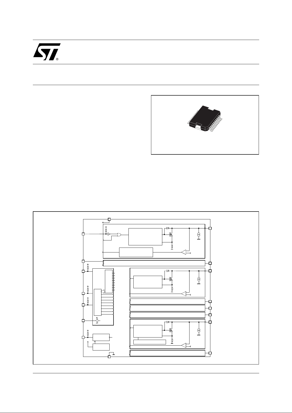
DESCRIPTION
L9825 is a Octal Low-Side Driver Circuit, dedicated
for automotive applications. Output voltage clamping
is provided for flyback current recirculation, when inductive loads are driven. Chip Select and Serial Peripheral Interface for outputs control and diagnostic
data transfer. Parallel Control inputs for two outputs.
BLOCK DIAGRAM
V
CC
V
CC
NON1
Q1
Diag1
NON2
V
Q2
CC
V
CC
V
CC
V
CC
V
CC
Diag2
SPI
Shift Register
V
CC
Reset
Undervoltage
RESET
NCS
CLK
SDI
SDO
nRES
July 2001
This is preliminary information on a new product now in development. Details are subject to change without notice.
Interface
Outp ut Latc h
GND
Q1
Q2
Q3
Q4
Q5
Q6
Q7
Q8
Diag1
Diag2
Diag3
Diag4
Diag5
Diag6
Diag7
Diag8
Reset
1
2
3
S
Latch / Driver
Fault Latch
S
Q3
Diag3
Q4
Diag4
Q5
Diag5
Q6
Diag6
S
Q7
Current Control
Overtemperature Detection
Diag7
Q8
Diag8
Latch / Driver
Latch / Driver
R
R
+
-
V
DG
CH1
CH2
R
+
-
V
DG
CH3
CH4
CH5
CH6
+
-
V
DG
CH7
CH8
OUT
I
OL
OUT
OUT
I
OL
OUT
OUT
OUT
OUT
I
OL
OUT
1/11
L9825
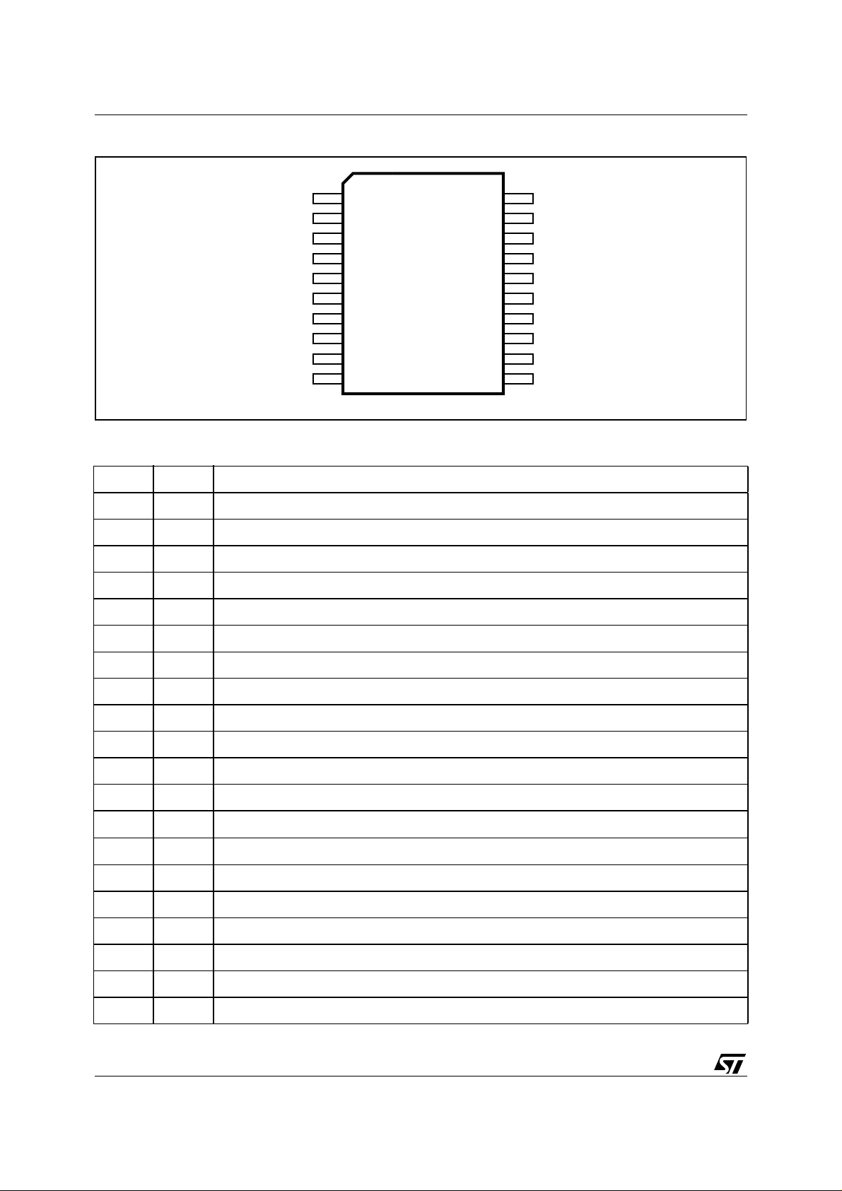
PIN CONNECTION
(Top view)
GND GND
NON1 NCS
SDO
OUT1
OUT3
OUT5
OUT7
SDI
CLK
GND
1
2
3
4
5
6
7
8
9
POWSO20
PIN DESCRIPTION
N° Pin Function
1 GND device ground
2 NON1 control input 1
3 SDO ser ial data outpu t
20
19
18
17
16
15
14
13
12
11
nRes
OUT8
OUT6
OUT4
OUT2
Vcc
NON2
GND10
4 Out 1 output 1
5 Out 3 output 3
6 Out 5 output 5
7 Out 7 output 7
8 SDI serial data input
9 CLK serial clock
10 GND device ground
11 GND device ground
12 NON2 control input 2
13 V
CC
supply voltage
14 Out 2 output 2
15 Out 4 output 4
16 Out 6 output 6
17 Out 8 output 8
18 nR es asynchronous nRes
19 NCS chip select (active low)
20 GND device ground
2/11
ABSOLUTE MAXIMUM RATINGS
For voltages and currents applied externally to the device:
Symbol Parameter Value Unit
L9825
V
CC
Inputs and data lines
V
IN
V
IN
I
IN
Supply voltage -0.3 to 7 V
(NONx, NCS, CLK, SDI, nRes)
Voltage (NONx, NCS, CLK, SDI) -0.3 to 7 V
Voltage (nRes) -0.3 to 7 V
Protection diodes current
1)
-20 to 20 mA
(T ≤ 1ms)
Outputs
Notes: 1. All inputs ar e protected against ESD according to MI L 883C; tested wi t h HBM at 2KV. It c orresponds to a dissipate d energy
(Out1 ... Out8)
V
I
E
OUTcl
OUTc
OUT
Continuous output voltage -1.0 to 45 V
Output current
Output clamp energy (I
E ≤ 0,2mJ.
2. Transient pul ses in accordance to DIN40839 part 1, 3 and ISO 7637 Pa rt 1, 3.
2)
≤ 0.5A) 20 mJ
OUT
-3 to 2.05 A
For currents determined within the device:
Outputs (Out1 ... Out8)
I
OUT
I
OUT
Output current (Out1 ... Out6) 2.05 A
Output current (Out7, Out8) 1.75 A
Total average-current all outputs
3. When oper ating the devi ce with short circuit at mor e than 2 outputs at the same tim e, damage due to electrical overstress m ay
occur.
3)
4.5 (Min.) A
THERMAL DATA
Symbol Parameter Value Unit
Thermal shutdown
T
JSC
Thermal resistance
R
thjc-one
R
thjc-all
Thermal shutdown threshold Min.
Typ.
150
165
Single output (junction case) Max. 13 °C/W
All outputs (junction case) Max. 1.6 °C/W
°C
°C
3/11
L9825
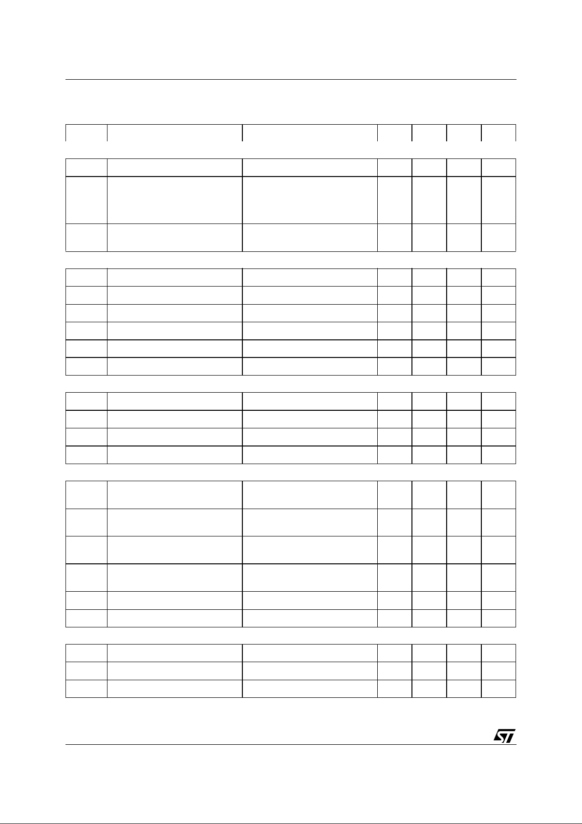
ELECTRICAL CHARACTERISTCS
(4.5V ≤ VCC ≤ 5.5V; -40°C ≤ TJ ≤ 150°C; unless otherwise specified)
Symbol Parameter Test Condition Min. Typ. Max. Unit
Supply voltage
I
ccSTB
I
ccOPM
∆I
Standby current without load 5 mA
Operating mode I
during reverse output
∆I
CC
CC
current
Inputs
(NONx. NCS, CLK, SDI, nRes)
V
V
V
R
C
Low level -0.3
INL
High level
INH
Hysteresis voltage 0.85 V
hyst
I
Input current VIN = V
IN
Pullup resistance 50 250 kΩ
IN
Input capacitanc e 10 pF
IN
Serial data outputs
V
SDOH
V
SDOL
I
SDOL
C
High output level I
Low output level I
Tristate leakage current NCS = high; 0V ≤ V
Output capacitance f
SDO
Outputs OUT 1 ... 8
OUT1 ... 8
= 500mA
5mA
SPI - CLK = 3MHz
NCS = LOW
SDO no load
I
= -3A 100 mA
out
0.2·V
CC
0.7·V
CC
CC
= -4mA
SDO
= 3,2mA 0.4 V
SDO
≤ V
SDO
= 300kHz 10 pF
SDO
CC
VCC -0.4
-10 10 µA
VCC+0.3
10 µA
V
V
V
I
OUTL1 - 8
I
OUTL1 - 8
I
OUTL1 - 8
V
R
DSon
C
Leakage current OUTx = OFF; V
Leakage current OUTx = OFF; V
Leakage current OUTx = OFF; V
Output clamp voltage 1mA ≤ I
clp
On resistance OUT 1 ... 8 I
Output capacitance V
OUT
Outputs short circuit protection
I
SBC
I
t
SCB
Overcurrent shutoff threshold OUT1 ... OUT6 1.05 1.4 2.05 A
Short circuit current limitation OUT7; OUT8 1.05 1.4 1.75 A
LIM
Delay shutdown for output 1 ... 6; I
4/11
= 25V; VCC =
OUTx
100 µA
5V
= 16V; VCC =
OUTx
100 µA
5V
= 16V; VCC =
OUTx
10 µA
1V
≤ I
; I
clp
outp
= 10mA
test
45 60 V
with correlation
= 500mA; Tj = +150°C 1.5 W
OUT
= 16V; f = 1MHz 300 pF
OUT
OUT
≤ 1/2 I
SBC
0.2 3 12 µs

L9825
ELECTRICAL CHARACTERISTCS
≤
(4.5V
VCC ≤ 5.5V; -40°C ≤ TJ ≤ 150°C; unless otherwise specified)
(continued)
Symbol Parameter Test Condition Min. Typ. Max. Unit
Diagnostics
V
I
Diagnostic threshold voltage
DG
Open load detection sink current V
OL
t
Diagnostic detection filter time for
df
out
= V
DG
0.32·V
CC
0.4·V
CC
20 100 µA
15 50 µs
output 1 & 2 on each diagnostic
condition
Outputs timing
t
don1
t
don2
t
dUon1/dt
dUon2/dt
dUoff1/dt
dUoff2/dt
Turn ON delay of OUT 1 and 2 NON
Turn ON delay of OUT 3 to 8 NCS = 50% to V
Turn OFF delay of OUT 1 to 8 NCS = 50% to V
doff
Turn ON voltage slew-rate For output 3 to 8; 90% to 30% of
Turn ON voltage slew-rate For output 1 and 2; 90% to 30%
Turn OFF voltage slew-rate For output 1 to 8; 30% to 90% of
Turn OFF voltage slew-rate For output 1 to 8; 30% to 80% of
Serial diagnostic link
NCS = 50% to V
NON
V
of V
V
V
(Load capacitor at SDO = 100pF)
= 50% to V
1, 2
= 50% to V
1, 2
; RL = 500Ω; V
bat
; RL = 500Ω; V
bat
; RL = 500Ω; V
bat
; RL = 500Ω; V
bat
OUT
OUT
OUT
OUT
= 0.9·V
= 0.9·V
= 0.1·V
OUT
= 16V
bat
bat
= 16V
bat
= 0.9 · V
bat
= 0.9·V
bat
bat
bat
= 0.1·V
= 16V
bat
bat
0.7 3.5 V/µs
2 10 V/µs
2 10 V/µs
2 15 V/µs
clp
5µs
10 µs
10 µs
V
f
clk
t
clh
t
cll
t
pcld
t
csdv
t
sclch
t
hclcl
t
scld
t
hcld
t
sclcl
t
hclch
t
pchdz
Clock frequency 50% duty cycle 3 MHz
Minimum time CLK = HIGH 160 ns
Minimum time CLK = LOW 160 ns
Propagation delay
4.9V ≤ VCC ≤ 5.1V 100 ns
CLK to data at SDO valid
NCS = LOW to data at SDO
100 ns
active
CLK low before NCS low
Setup time CLK to NCS change H/L
100 ns
CLK change L/H after NCS = low 100 ns
SDI input setup time CLK change H/L after SDI data
20 ns
valid
SDI input hold time
SDI data hold after CLK change H/L
20 ns
CLK low before NCS high 150 ns
CLK high after NCS high 150 ns
NCS L/H to output data float 100 ns
NCS pulse filter time Multiple of 8 CLK cycles
5/11

L9825
FUNCTIONAL DESCRIPTION
General
The L9825 integrated circuit features 8 power low-side-driver outputs. Data is transmitted to the device using
the Serial Peripheral Interface, SPI protocol. Outputs 1 and 2 can be controlled parallel or serial. The power
outputs features voltage clamping function for flyback current recirculation and are protected against short circuit to Vbat.
The diagnostics recognizes two outputs fault conditions: 1) ov ercurr ent for outpu ts 1 to 6 , over curr ent and thermal overload for outputs 7 and 8 in switch-on co ndition and 2) open load or short to GND in switch- off condition
for all outputs. The outputs status can be read out via the serial interface.
The chip internal reset is a OR function of the external nRes signal and internally generated undervoltage nRes
signal.
Output Stages Control
Each output is controlled with its latch and with common reset line, which enables all eight outputs. Outputs 1
and 2 can be controlled also by its NON1, NON2 inputs. It allows PWM control independently on the SPI. These
inputs features internal pull-up resistors to assure that the outputs are switched off, when the inputs are open.
The control data are transmitted via the SDI input, the timing of the serial interface is shown in Fig. 1.
The device is selected with low NCS signal and the input data are transferred into the 8 bit shift register at every
falling CLK edge. The rising edge of the NCS latches the new data from the shift register to the drivers.
Figure 1. Timin g of the Serial Interface
NCS
tsclch thclcl tclh tcll tsclcl thclch
CLK
tcsdv tpcld tpchdz
SDO
SDI
not defined D8 D1
tscld
thcld
D8 D7 D1
The SPI register data are transfer red to the output l atch at r ising N CS edge. The digital filter between NCS and
the output latch ensures that the data are transferred only after 8 CLK cycles or multiple of 8 CLK cycles since
the last NCS falling edge. The NCS changes only at low CLK.
Table 1. Outputs Control
Outputs 1, 2: Outputs 3 to 8:
NON1,2 1 0 0 1
SPI-bit 1,2 0 0 1 1 SPI-bit 3...8 0 1
Output 1, 2 off on on on Output 3...8 off on
6/11

L9825
Figure 2.
Output Control register structure
MSB LSB
Q2 Q4 Q6 Q8 Q1 Q3 Q5 Q7
Control-bit output 7
Control-bit output 5
Control-bit output 3
Control-bit output 1
Control-bit output 8
Control-bit output 6
Control-bit output 4
Control-bit output 2
Power outputs characteristics for flyback current, outputs short circuit protection and diagnostics
For output currents flowing into the circuit the output vol tages are limited. The ty pical value of this vo ltage is 50V.
This function allows that the flyback current of a inducti ve load r ecircul ates into the circui t; the flyback energy is
absorbed in the chip.
Output short circuit protection for outputs 1 to 6 (dedicated for loads without inrush current): when the output
current exceeds the short circuit threshold, the corresponding output overload latch is set and the output is
switched off immediately.
Output short circuit protection for outputs 7 and 8 (dedicated for loads with inrush current, as lamps): when the
load current would exceed the short circuit limit value, the corresponding output goes in a current regulation
mode. The output current is determined by the output characteristics and the output voltage depends on the
load resistance. In this mode high power is dissipated in the output transis tor and its temperatur e increases rapidly. When the power transistor temperatur e exceeds the thermal shutdow n threshold, the ov erload latch is set
and the corresponding output switched off.
For the load diagnostic in output off condition each output features a diagnostic current sink, typ 60µA.
Diagnostics
The output voltage at all outputs is compared with the diagnostic threshold, typ 0.38 · V
.
CC
Outputs 1 and 2 features dedicated fault latches. The output status signal is filtered and latched. The fault latches are cleared dur ing NCS low. The latch stores the status bi t, so the first reading after the er ror occ urred might
be wrong. The second reading is right.
Table 2. Diagnostic for outputs 1 and 2
Output 1, 2 Output-voltage Status-bit Output-mode
off > DG-threshold high correct operation
off < DG-threshold low fault condition 2)
on < DG-threshold high correct operation
on > DG-threshold low fault condition 1)
Fault condition 1) "output short circuit to Vbat" : the output was switched on and the voltage at the output exceeded the diagnostics threshold due to overcurrent, the output overload latch was set and the output has been
switched off. The diagnostic bit is low.
7/11

L9825
g
g
g
g
g
g
Fault condition 2) "open load" or "output short circuit to GND" : the output is switched off and the voltage at the
output drops below the diagnostics threshold, because the load current is lower than the output diagnostic current source, the load is interrupted. The diagnostic bit is low.
For outputs 3 to 8 the output status signals, are fed directly to the SPI register.
Table 3. Diagnostic for outputs 3 to 8
Output 3 ... 8 Output-voltage Status-bit Output-mode
off > DG-threshold high correct operation
off < DG-threshold low fault condition 2)
on < DG-threshold high correct operation
on > DG-threshold low fault condition 1)
The fault condition 1) "output short circuit to Vbat" :
For outputs 3 to 6 is the same as of outputs 1 and 2.
For outputs 7 and 8 : the output was switched on and the voltage at the output exceeds the diagnostics thresh-
old. The output operates in current regulation mode or has been switched off due to thermal shutdown. The status bit is low.
Fault condition 2) "open load" or "output short circuit to GND" is the same as of outputs 1 and 2.
At the falling edge of NCS the output status data are transferred to the shift register. When NSC is low, data bits
contained in the shift register are transferred to SDO output et every rising CLK edge.
Figure 3. The Pulse Diagram to Read the Outputs Status Register
NCS
CLK
SDI
SDO
MSB
654321
MSB
654321
Figure 4. The Structure of the Outputs Status Register
MSB LSB
Diag2 Diag4 Diag6 Diag8 Diag1 Diag3 Diag5 Diag7
Dia
Diagnostic-bit output 5
Dia
Dia
Diagnostic-bit output 8
Dia
Dia
Dia
LSB
LSB
nostic-bit output 7
nostic-bit output 3
nostic-bit output 1
nostic-bit output 6
nostic-bit output 4
nostic-bit output 2
8/11

APPLICATION NOT ES
Figure 5. Typical Application Circuit Diagram
L9825
L9825
L9825
For higher current driving capability two outputs of the same kind can be paralleled. In this case the maximum
flyback energy should not exceed the limit value for single output.
The immunity of the circuit with respect to the transients at the output is verified during the characterization for
Test Pulses 1, 2 and 3a, 3b, DIN40839 or ISO7637 part 3. The Test Pulses are coupled to the outputs with
200pF series capacitor. All outputs withstand testpulses without damage.
The correct function of the c ircuit with t he Test Pulses coupled to the outputs is ver ified d uring the ch aracter ization for the typical application wi th R = 16W to 200W, L= 0 to 600mH loads. The Test Pulses are coupled to the
outputs with 200pF series capacitor.
9/11

L9825
DIM.
MIN. TYP. MAX. MIN. TYP. MAX.
mm inch
A 3.6 0.142
a1 0.1 0.3 0.004 0.012
a2 3.3 0.130
a3 0 0.1 0.000 0.004
b 0.4 0.53 0.016 0.021
c 0.23 0.32 0.009 0.013
D (1) 15.8 16 0.622 0.630
D1 9.4 9.8 0.370 0.386
E 13.9 14.5 0.547 0.570
e 1.27 0.050
e3 11.43 0.45 0
E1 (1) 10.9 11.1 0.429 0.437
E2 2.9 0.114
E3 5.8 6.2 0.228 0.244
G 0 0.1 0.000 0.004
H 15.5 1 5.9 0.610 0.626
h 1.1 0.043
L 0.8 1.1 0.031 0.043
N 10˚ (max.)
S
8˚ (max.)
T10 0.394
(1) "D and F" do not include mold flash or protrusions.
- Mold flash or protrusions shall not exceed 0.15 mm (0.006").
- Critical dimensions: "E", "G" and "a3"
OUTLINE AND
MECHANICAL DATA
JEDEC MO-166
PowerSO20
E2
h x 45
DETAIL B
BOTTOM VIEW
R
lead
a3
Gage Plane
E
DETAIL B
0.35
S
D1
L
c
a1
DETAIL A
slug
- C -
SEATING PLANE
GC
(COPLANARITY)
E3
NN
a2
A
b
DETAIL A
e3
H
D
T
1
e
1120
E1
10
PSO20MEC
10/11

L9825
Information furnished is believed to be accurate and reliable. However, STMicroelectronics assumes no responsibility for the consequences
of use of such information nor for any infringement of patents or other rights of third parties which may result from its use. No license is granted
by implic ation or oth erwise under any patent or patent rights of STMicroel ectronics. S pecificati ons mentioned in this publicati on are subje ct
to change without notice. This publication supersedes and replaces all information previously supplied. STMicroelectronics products are not
authorized for use as critical components in life support devices or systems wi t hout express written approval of STMicroelectro nics.
The ST logo is a registered trademark of STMicroelectronics
2001 STMi croelectr oni cs - All Rights Reserved
Australi a - Brazil - Chin a - Finland - France - Germany - Hong Ko ng - India - Italy - Ja pan - Malaysia - Mal ta - Morocco - Sin gapore - Spai n
STMicroelectronics GROUP OF COMPANIES
- Sweden - Sw itzerland - United Kingdom - U.S.A.
http://www.s t. com
11/11
 Loading...