

L9823
Octal Low-Side Driver for bulb, resistive and inductive loads with
serial input control, output protection and diagnostic
■ OUTPUTS CURRENT CAPABILITY UP TO
0.5A
■ CASCADABLE SPI CONTROL FOR
OUTPUTS
■ RESET FUNCTION WITH RESET SIGNAL OR
UNDERVOLTAGE AT V
■ PROGRAMM ABLE INTRINSIC OUTPUT
VOLTAGE CLAMPI N G AT TYP. 5 0V FOR
INDUCTIVE SWITCHING
■
OVERCURRENT SHUTDOWN WITH LATCHOFF FOR EVERY WRITE CYCLE (SFPD = LOW)
■ INDEPENDENT THERMAL SHUTDOWN OF
OUTPUTS (SOA PROTECTION)
■
OUTPUT STATUS DATA AVAILABLE ON THE
SPI USING 8-BIT I/O PROTOCOL UP TO 3.0 MHZ
■ LOW STANDBY CURRENT WITH RESET =
LOW (TYP 35µA @ VDD)
■ OPEN LOAD DETECTION (OUTPUTS OFF)
■ SINGLE V
LOGIC SUPPLY
DD
■ HIGH EMS IMMUNITY AND LOW EME
(CONTROLL ED OU T P UT S LOP E S)
■ FULL FUNCTIONALITY OF THE REMAINING
DEVICE AT NEGATIVE VOLTAGE DROP ON
DD
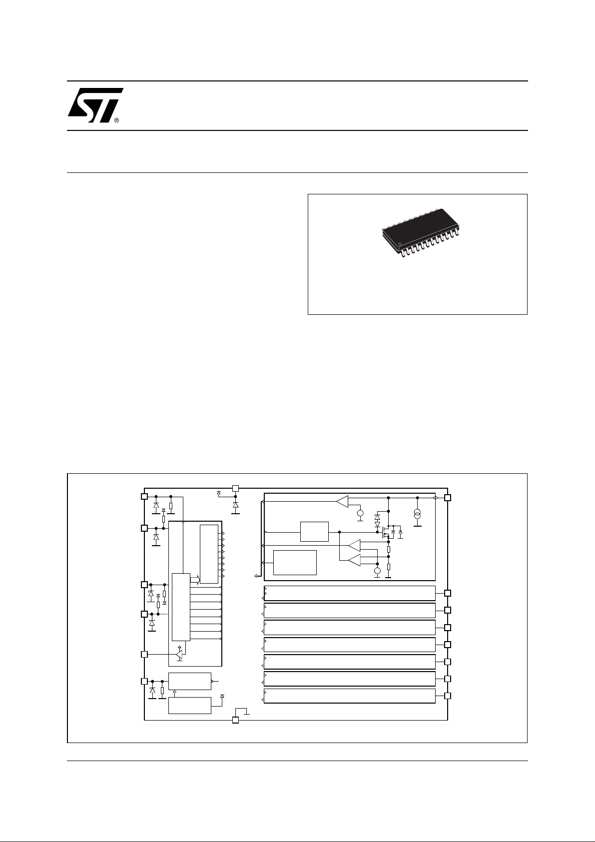
SO24 (20+2+2)
ORDERING NUMBER: L9823
OUTPUTS (-1,5V OR -3,0A)
■ OUTPUT MODE PROGRAMMABLE FOR
SUSTAINED CURRENT LIMIT OR
SHUTDOWN
DESCRIPTION
L9823 is a Octal Low-Side Driver Circuit, dedicated
for automotive applications. Output voltage clamping
is provided for flyback current recirculation, when inductive loads are driven. Chip Select and cascadable
Serial 8-bit Interface for outputs control and diagnostic data transfer.
BLOCK DIAGRAM
SFPD
15
CSB
10
SCLK
3
SI
4
SO
9
Reset
22
April 2003
SPI
Interface
Shif t Register
Reset
Undervoltage
RESET
V
16
DD
OL0
Q0
Q0
Q1
I
SCB
Diag0
Diag1
Diag2
Diag3
Diag4
Diag5
Diag6
Diag7
GND
0
OT0
Q1
Q2
Q3
Q4
Q5
Q6
Q7
17 - 20
Q2
Q3
Q4
Q5
Q6
Q7
Output Latch
Diag0
Diag1
Diag2
Diag3
Diag4
Diag5
Diag6
Diag7
Reset
5 -8
Over
Temperature
Detect
Gate
Control
+
V
DG
=
+
-
+
=
I
OL
CH0
CH1
CH2
CH3
CH4
CH5
CH7
CH7
OUT0
24
OUT1
23
OUT2
14
OUT3
13
OUT4
12
OUT5
11
OUT6
2
OUT7
1
1/12
L9823
PIN FUNCTION
N° Pin Description
1 Out 7 Output 7
2 Out 6 Output 6
3 SCLK SCLK. The system clo ck pin (SCLK) clocks the inte rnal shift registers of the L98 23. The serial
input pin (SI) accepts data into the input shift register on the falling edge of the SCLK signal while
the serial output pin (SO) shifts data information out of the shift register on the rising edge of the
SCLK signal. False clocking of the shift register must be avoided to guarantee validity of data. It
is essential that the SCLK pi n be in a log ic low state w hene ver chip select bar pin (CSB) ma kes
any transition . For th is reason , it is r ecommend ed thoug h not n ecessary, that the SC LK pin be
kept in a low logic state as long as th e device i s not acce ssed (CSB in logic h igh state). Wh en
CSB is in a logic h igh state, any signal a t the SCLK and SI p in is ignored and SO is tri- stated
(high-impedan ce).
4 SI SI. This pin is fo r the input of ser ial ins tructio n data. SI informati on is r ead in on th e fall ing ed ge
of SCLK. A logic high state present on this pin when the SCLK signal rises will program a
specific output O FF, and in turn, turns OFF the specific output on the r ising edge of the CSB
signal. Converse ly, a logic low state present on the SI pin wi ll program the output ON, and in
turn, turns ON th e specific output on the rising edge of the CSB s ignal. To program the eight
outputs of the L9823 ON or O FF, an eight bit serial stream of data is req uired to be en tered into
the SI pin starting with Outp ut 7, follo wed by Outpu t 6, Output 5, etc., to Outpu t 0. For eac h rise
of the SCLK signal, with CSB held in a logic low state, a databit instruction (ON or OFF) is
loaded into t he shift registe r per the da tabit SI state. The shift register i s full after eig ht bits of
information have be en ente red. To preserve data integrity, care should be taken to not transition
SI as SCLK transitions from a low-to-high logic state.
5 GND GND
6 GND GND
7 GND GND
8 GND GND
9 SO SO. The serial output (SO) pin is the tri-stateable outp ut from the shift register. The SO pin
remains in a high impe dance state until the CSB pin goes to a logic lo w state. The SO data
reports the drain status, either high or low. The SO pin changes state on the rising edge of SCLK
and reads out on the falling edge of SCLK. When an output is OFF and not faulted, the
corresponding SO databit is a high state. When SO an output is ON, and there is no fault, the
corresponding databit on the SO pin will be a low logic state. The SI / SO shifting of data follows
a first-in-first-out prot ocol with both input and outpu t words transferring the Most Significant Bit
(MSB) first. The SO pin is not affected by the status of the Reset pin.
10 CSB CSB. The system MC U sele cts the L982 3 to be com mun icated with through the use of the CSB
pin. Whenever the pin is in a logic low state, data can be transferred from the MCU to the L9823
and vise versa. C locked-in data from th e MCU is transferre d from the L9823 s hift register and
latched into the powe r outputs o n the ris ing edge of the C SB signa l. On the falling edge of the
CSB signal, dra in status information is transferred fro m the power outp uts and loaded into the
device's shift register. The CSB pin also controls the output driver of the serial output pin.
Whenever the CSB pin goes to a logic low state, the SO pin output driver i s enabled allow ing
information to be transferred from the L9823 to the MCU. To avoid any spurious data, it is
essential that the high-to-low transition of the CSB signal occur only when SCLK is in a logic low
state.
11 Out 5 Output 5
12 Out 4 Output 4
13 Out 3 Output 3
2/12
L9823
PIN FUNCTION
(continued)
N° Pin Description
14 Out 2 Output 2
15 SFPD SFPD. The Short Fault Protect Disable (SFPD) pin is used to disable the overcurrent latch-OFF.
This feature allow s control of incandescent load s where in-rush currents exceed the devi ce's
analog current limits. Essentially the SFPD pin determines whether the L9823 output(s) will
instantly shutdown upon sensing an ou tput short or remain ON in a current limiting m ode of
operation until the output short is removed or thermal shutdown is reac hed. If the SFPD pin is
tied to V
the L9823 output(s) will remain ON in a curr ent limited mode of operation upon
DD
encountering a loa d short to supply. If the SFPD pin is grounded, a sh ort circu it will imm edia tely
shutdown only the output affected. Other outputs not having a fault condition will operate
normally.
16 VDD VDD
17 GND GND
18 GND GND
19 GND GND
20 GND GND
21 NC Not Connected
22 Reset Reset. The Reset pin is active low and used to clear the SPI shift register and in doing so sets all
output switches OF F. With the device in a system with an MCU; upon initial syste m power up,
the MCU h olds the Reset p in of the device i n a logic low state ensuring all outpu ts to be O FF
until the VDD pin voltages are adeq uate for p redic table operatio n. A fter th e L9 823 is Re set, the
MCU is ready to assert system cont rol with all output swi tches initially OFF. The Reset pin is
active low and has an internal pull-down incorpora ted to ensure operational predic tability
should the e xterna l pul l-dow n of the MCU open circ uit. T he in terna l pul l-up i s to afford s afe a nd
easy interfacing to the MCU. The Reset pin of the L9823 should be pulled to a logic low state for
a duration of at least 160ns to ensure reliable Reset.
23 Out 1 Output 1
24 Out 0 Output 0
ABSOLUTE MAXIMUM RATINGS
For voltages and currents applied externally to the device. Exceeding limits may cause damage to the device
Symbol Parameter Value Unit
V
DD
Inputs and data lines
(CSB, SCLK, SI, Reset, SFPD, SO)
V
IN
V
SDO
I
IN
Outputs (Out0 ... Out7)
V
OUT Cont
Supply voltage -0.3 to 7 V
Voltage
-0.3 to 7
(CSB, SCLK, SI, Reset, SFPD)
Voltage (SO) -0.3 to VDD+0.3 V
Protection diodes current
1)
T ≤ 1ms -20 to 20
1)
mA
Continuous output voltage -1.5 to 45 V
3/12
.
L9823
ABSOLUTE MAXIMUM RATINGS
(continued)
Symbol Parameter Value Unit
V
OUT Cont
I
OUT PEAK
E
OUTclamp
I
OUT LIM
Note 1) All inputs are protected against ESD according to MIL 883C; tested with HBM C = 100pF, R = 1500Ω at ±2KV. It corresponds to
Continuous output current -3 to I
Output current
Output clamp energy
3)
OUT LIM
2)
to 2
-10
50 mJ
Output current (self limit) 2 A
a dissipat ed energy E ≤ 0.2mJ (data avail abl e upon reques t ).
2) Transient pulses in accordance to DIN40839 part 1, 3 and ISO 7637 Part 1, 3.
3) Max. output clamp energ y at T
= 150°C, using single non-repetitive pulse of 500mA
j
A
A
THERMAL DATA
Symbol Parameter Value Unit
Thermal shutdown
T
LIM
Thermal resistance (junction-to-Lead)
R
thjL-one
R
thjL-all
Thermal shutdown threshold 155 (Min.), 180 (Typ.) °C
Single output (junction lead) 25 (Max.) °C/W
All outputs (junction lead) 20 (Max.) °C/W
T
stg
ELECTRICAL CHARACTERISTCS
Storage Temperature -55 to 150 °C
(4.5V ≤ VDD ≤ 5.5V; -40°C ≤ TJ ≤ 150°C; unless otherwise specified
Symbol Parameter Test Condition Min. Typ. Max. Unit
Supply voltage
I
DDSTB
I
DDleak
I
DDOPM
Standby current
leakage current
Operating mode I
Reset = LOW and / or
V
DDRES>VDD
V
< 0.5V
DD
OUT0 ... 7
> 0.5V
= 500mA
35
<1
70
10
6mA
SPI - SCLK = 3MHz
CSB = LOW
SO no load
∆I
DD rev∆IDD
during reverse output
I
= -2.5A 10 mA
out rev
current
V
DD RES
Undervoltage Reset Reset of all registers and disable
2.5 3.95 V
of all outputs
Inputs (CSB, SCLK, SI, Reset, SFPD)
V
V
Low level -0.3
INL
High level
INH
0.7·V
DD
0.2·V
DD
VDD+0.3
µA
µA
V
V
4/12
V
Hysteresis voltage 0.5 1.2
hyst
0.5·V
DD
V

L9823
ELECTRICAL CHARACTERISTCS
(continued)
Symbol Parameter Test Condition Min. Typ. Max. Unit
I
Input current VIN = V
IN
R
Pullup resistance
IN
DD
-10 10 µA
50 250 kΩ
(CSB, SI)
Pulldown resistance
(SFPD, Reset, SCLK)
C
Input capacitance 10 pF
IN
Serial data outputs
V
V
SOH
SOL
I
SOL
C
High output level ISO = -4mA
Low output level ISO = 3,2mA 0.4 V
Tristate leakage current CSB = high; 0V ≤ VSO ≤ V
Output capacitance fSO = 300kHz, 0V ≤ VSO ≤ V
SO
DD
DD
VDD -0.4
-10 10 µA
20 pF
Outputs OUT 0 ... 7
I
OUTL0 - 7
V
OUT
clamp
Leakage current OUTx = OFF; V
VDD ≤ V
DD RES
Tj ≤ 85°C
Output clamp voltage 2mA ≤ I
I
OUT clamp
= 20mA with correlation
OUT test
= 16V;
OUTx
and / or Reset = Low
≤ I
OUT LIM
-10
10 µA
<1µA
45 60 V
V
R
C
DSon
On resistance OUT 0 ... 7 I
Output capacitance V
OUT
Outputs short circuit protection
I
SCB
I
OUT LIM
t
dly SCB
Overcurrent shutoff threshold SFPD = Low, V
Short circuit current limitation 0.5 1.6 2.5 A
Short circuit shutdown delay SFPD = Low, V
Diagnostics
V
I
OUT OL
t
dly SFPD
Diagnostic threshold voltage
DG
Open load detection sink current V
Diagnostic detection filter time SFPD = Low, V
Outputs timing
don
Turn ON delay CSB = 50% to RL = 50Ω
t
= 500mA;Tj = +150°C
OUT
Tj = +25°C
= 16V; f = 1MHz 300 pF
OUT
OUT
OUT
≥ V
≥ V
DG
DG
0.5 1.6 2.5 A
70 150 250 µs
1
0.8
CSB = 50% to
I
OUT
≤ 1/2 I
OUT LIM
0.5·VDD0.55·VDD0.6·V
out
= V
DG
30 60 100 µA
Output programmed OFF
OUT
≥ V
DG
70 150 250 µs
CSB = 50% to
valid data at SO
V
OUT
= 0,9V
bat
, V
bat
= 16V
1.5
1.25
DD
20 µs
Ω
Ω
V
5/12

L9823
ELECTRICAL CHARACTERISTCS
(continued)
Symbol Parameter Test Condition Min. Typ. Max. Unit
t
dV
dV
dV
clamp/dt
doff
on/dt
off/dt
Turn OFF delay CSB = 50% to RL = 50Ω
V
= 0,1·V
OUT
Turn ON voltage slew-rate 90% to 30% of V
RL = 50Ω; V
Turn OFF voltage slew-rate 30% to 90% of V
RL = 50Ω; V
Turn OFF voltage clamp slew-rate 30% to 80% of V
off
RL = 500Ω
bat
bat
bat
, V
bat
;
bat
= 16V
;
bat
= 16V
OUT clamp
20 µs
= 16V
0.7 2.1 3.5
0.7 2.1 3.5
0.7 2.1 5.5
Serial diagnostic link (Load capacitor at SO = 200pF)
sclk
clh
t
cll
pcld
Clock frequency 50% duty cycle 3 MHz
Minimum time SCLK = HIGH 160 ns
Minimum time SCLK = LOW 160 ns
Propagation delay
4.9V ≤ VDD ≤ 5.1V 100 ns
f
t
t
SCLK to data at SO valid
t
csdv
t
sclch
CSB = LOW to data at SO active 100 ns
SCLK low before CSB low Setup time SCLK to CSB change
100 ns
H/L
V/µs
V/µs
V/µs
t
hclcl
SCLK change L/H after CSB =
Low
t
t
t
sclcl
t
hclch
t
pchdz
t
Reset
scld
hcld
SI input setup time SCLK change H/L after SI data
SI input hold time SI data hold after SCLK change
SCLK low before CSB high 150 ns
SCLK high after CSB high 15, ns
CSB L/H to output data float 100 ns
Minimum Reset time Reset = Low 160 ns
Outputs Control Tables :
Setup time CSB to SCLK change
L/H
valid
H/L
Outputs:
SI-bit 0 1
Output on off
100 ns
20 ns
20 ns
6/12

Output Control register structure :
MSB LSB
L9823
Q7
Q0Q1Q2Q3Q4Q5Q6
Control-bit output 7
Control-bit output 6
Control-bit output 5
Control-bit output 4
Control-bit output 3
Control-bit output 2
Control-bit output 1
Control-bit output 0
Power outputs characteristics
for flyback current, outputs short circuit protection and diagnostics
For output currents flowing into the circuit the output voltages are limited. The typical value of this voltage is 50V.
This function allows that the flyback current of a inductive load recirculates into the circuit; the flyback energy is
absorbed in the chip.
Output short circuit protection SFPD = Low (dedicated for loads without inrush current): when the output current
exceeds the short circuit threshold, the corresponding output overload latch is set after a delay time t
dly SCB
and
the output is switched off. The delay timer is started af ter each rise of CSB and v alid datas are transfered to the
output control register. If the short takes place after the delay time has elapsed the shutdown is immediate (within 15µs).
Output short circuit protection SFPD = High (dedicated for loads with inrush current, as lamps): when the load
current would exceed the short circuit limit value, the corresponding output goes in a current regulation mode.
The output current is determined by the output characteristics and the output voltage depends on the load resistance. In this mode high power is dissipat ed in the output transistor and it s temperature increases rapi dly.
When the power transistor temperature exceeds the thermal shutdown threshold, the overload latch is set and
the corresponding output switched off.
For the load diagnostic in output off condition each output features a diagnostic current sink, of typ 60µA.
FUNC TIONAL DESCRIPTION
General
The L9823 integrated circuit features 8 power low-side-driver outputs. Data is transmitted to the device using
the Serial Peripheral Interface = SPI protocol. The power outputs features voltage clamping function for flyback
current recirculation and are protected against short circuit to Vbat.
The diagnostics recognizes two outputs fault conditions: 1) overcurrent and thermal overload in switch-ON condition and 2) open load or short to GND in switch-OFF condition for all outputs. The outputs status can be read
out via the serial interface.
The chip internal Reset is a OR function of the external Reset signal and internally generated undervoltage Reset signal.
7/12

L9823
Output Stages Control
Each output is controlled with its latch and with a common Reset line, which enables all outputs.
The control data are transmitted via the SI input, the timing of the serial interface is shown in Fig. 1.
The device is selected with low CSB signal and the input data are transferred into the 8 b it shift register at every
falling SCLK edge. The rising edge of the CSB latches the new data from the shift register to the drivers.
Figure 1. Timin g of the Serial Interface
CSB
SCLK
SO
tsclch thclcl tcl h
tcsdv tpcld tpchdz
not defined D7 D0
tscld
SI
tcll
thcld
D7 D6 D0
tsclcl thclch
The SPI register data are transferred to the output latch at rising CSB edge. The digital filter between CSB and
the output latch ensures that the data are transferred only after 8 SCLK cycles or multiple of 8 SCLK cycles
since the last CSB falling edge. The CSB changes only at low SCLK.
Diagnostics
The output voltage at all outputs is compared with the diagnostic threshold, typ 0,55 • VDD = VDG.
Diagnostic Table for outputs:
Output Output-voltage Status-bit Output-mod e
off > DG-threshold high correct operation
off < DG-threshold low fault condition 2)
on < DG-threshold low correct operation
on > DG-threshold high fault condition 1)
Fault condition 1) "output short circuit to Vbat" : For SFPD = Low the output was switched on and the voltage at
the output exceeded the diagnost ics thr eshold due to overc urrent, the output overl oad latch was set and the
output has been switched off. The diagnostic bit is high.
: For SFPD = High the output was switched on and the voltage at the output exceeds the diagnostics threshold.
The output operates in current regulation mode or has been switched off due to thermal shutdown. The status
bit is high.
Fault condition 2) "open load" or "output short circuit to GND" : the output is switched off and the voltage at the
output drops below the diagnostics threshold, because the load current is lower than the output diagnostic current source, the load is interrupted. The diagnostic bit is low.
At the falling edge of CSB the output status data are transferred to the shift register. When SCB is low, data bits
contained in the shift register are transferred to SO output at every rising SCLK edge.
8/12

Figure 2. Pulse Diagram to Read the Outputs Status Register
u
u
u
u
u
u
u
u
CSB
SCLK
L9823
SI
SO
MSB
MSB
5
65
Figure 3. Structure of the Outputs Status Register
MSB
43
4
32
LSB
Diag0Diag1Diag2Diag3Diag4Diag5Diag6Diag7
2
LSB6
1
1
LSB
Diagnostic-bit o
Diagnostic-bit o
Diagnostic-bit o
Diagnostic-bit o
Diagnostic-bit o
Diagnostic-bit o
Diagnostic-bit o
Diagnostic-bit o
9/12

L9823
T
APPLICATIONS INFORMATION
The typical application diagram for parallel Input SPI control is shown in Figure 4.
Figure 4. Typical Application Circuit Diagram for the L9823 Circuit.
µP
V
DD
V
16
SFPD
15
CSB
10
SPI
Interface
SCLK
3
SI
4
Shift Register
SO
9
Reset
22
SI
SO
SCLK
CSB2 ... 7
Reset
Reset
Undervoltage
RESET
DD
OL0
Over
Temperature
Detect
Gate
Control
Q0
Q0
Q1
I
0
Q2
SCB
Q3
Q4
OT0
Q5
Q6
Q7
Output Latch
Diag0
Diag0
Q1
Diag1
Diag1
Diag2
Q2
Diag3
Diag2
Diag4
Diag5
Q3
Diag6
Diag3
Diag7
Q4
Diag4
Q5
Diag5
Q6
Reset
Diag6
Q7
Diag7
-
+
V
DG
=
+
-
+
=
U459
5 -8
GND
17 - 20
I
OL
CH0
CH1
CH2
CH3
CH4
CH5
CH7
CH7
VOLTAGE
REGULATOR
OUT0
24
OUT1
23
OUT2
14
OUT3
13
OUT4
12
OUT5
11
OUT6
2
OUT7
1
R, L loads
V
BA
U459
For higher current driving capability more outputs of the same kind can be paralleled. In this case the maximum
flyback energy should not exceed the limit value for single output.
The immunity of the circuit with respect to the transients at the output is verified during the characterization for
Test Pulses 1, 2 and 3a, 3b, DIN40839 or ISO7637 part 3. The Test Pulses are coupled to the outputs with
200pF series capacitor. The correct function of the circuit with the Test Pulses coupled to the outputs is verified
during the characterization for the t ypi cal appl icati on wit h R = 16
Ω
to 200Ω, L= 0 to 600mH loads. All outputs
withstand testpulses without damage.
10/12

L9823
DIM.
MIN. TYP. MAX. MIN. TYP. MAX.
A 2.35 2.65 0.093 0.1 04
A1 0.10 0.30 0.004 0.012
B 0.33 0.51 0.013 0.2 00
C 0 .23 0.32 0.009 0.013
(1)
15.20 15.60 0.598 0.614
D
E 7.40 7.60 0.291 0.299
e 1.27 0.050
H 1 0.0 10.65 0.394 0.419
h 0.25 0;75 0.010 0.030
L 0.40 1.27 0.016 0.050
k 0˚ (min.), 8˚ (max.)
ddd 0.10 0.004
(1) “ D” dime nsion d o es not i nclud e m ol d flash, pr ot usion s or ga t e
burrs. Mo ld f las h, p rotus ion s or g at e bur rs sh all not exce ed
0.15mm per side.
mm inch
OUTLINE AND
MECHANICAL DATA
Weight: 0.60gr
SO24
0070769 C
11/12

L9823
Information furnished is believed to be accurate and reliable. However, STMicroelectronics assumes no responsibility for the consequences
of use of such information nor for any infringement of patents or other rights of third parties which may result from its use. No license is granted
by implic ation or otherwise under any paten t or patent r i ghts of STMicroelectroni cs. Specifications me ntioned in this publicat i on are subje ct
to change without notice. This publication supersedes and replaces all information previously supplied. STMicroelectronics products are not
authorized for use as crit i cal component s i n l i f e support devices or systems wi thout express written approval of STMic roelectronics.
The ST logo is a registered trademark of STMicroelectronics
2003 STMicroelectr oni cs - All Rights Reserved
Austra lia - Brazil - Canada - China - Fi nl and - France - G erm any - Hong Kong - India - Israel - I taly - Japan -Malaysia - Mal ta - Morocco -
Singap ore - Spain - Sweden - Switzerl and - United Ki ngdom - United States.
STMicroelectronics GROUP OF COMPANIES
http://www.s t. com
12/12
 Loading...