SGS Thomson Microelectronics L9822N Datasheet

L9822N
OCTALSERIAL SOLENOID DRIVER
.EIGHTLOWR
(0.5ΩATI
=1A@25°CVCC=5V±5%)
O
DMOSOUTPUTS
DSon
.8 BITSERIAL INPUT DATA (SPI)
.
8 BIT SERIAL DIAGNOSTIC OUTPUT FOR
OVERLOADANDOPENCIRCUITCONDITIONS
.
OUTPUT SHORT CIRCUITPROTECTION
.CHIPENABLESELECTFUNCTION(activelow)
.INTERNAL 35V CLAMPINGFOR EACH OUT-
PUT
.CASCADABLE WITH ANOTHER OCTAL
DRIVER
.LOWQUIESCENTCURRENT (10mAMAX.)
.
PACKAGE PowerSO20
DESCRIPTION
TheL9822N is an octal low side solenoiddriver
realizedin Multipower-BCDtechnologyparticularly
suitedfor drivinglamps,relaysandsolenoidsin au-
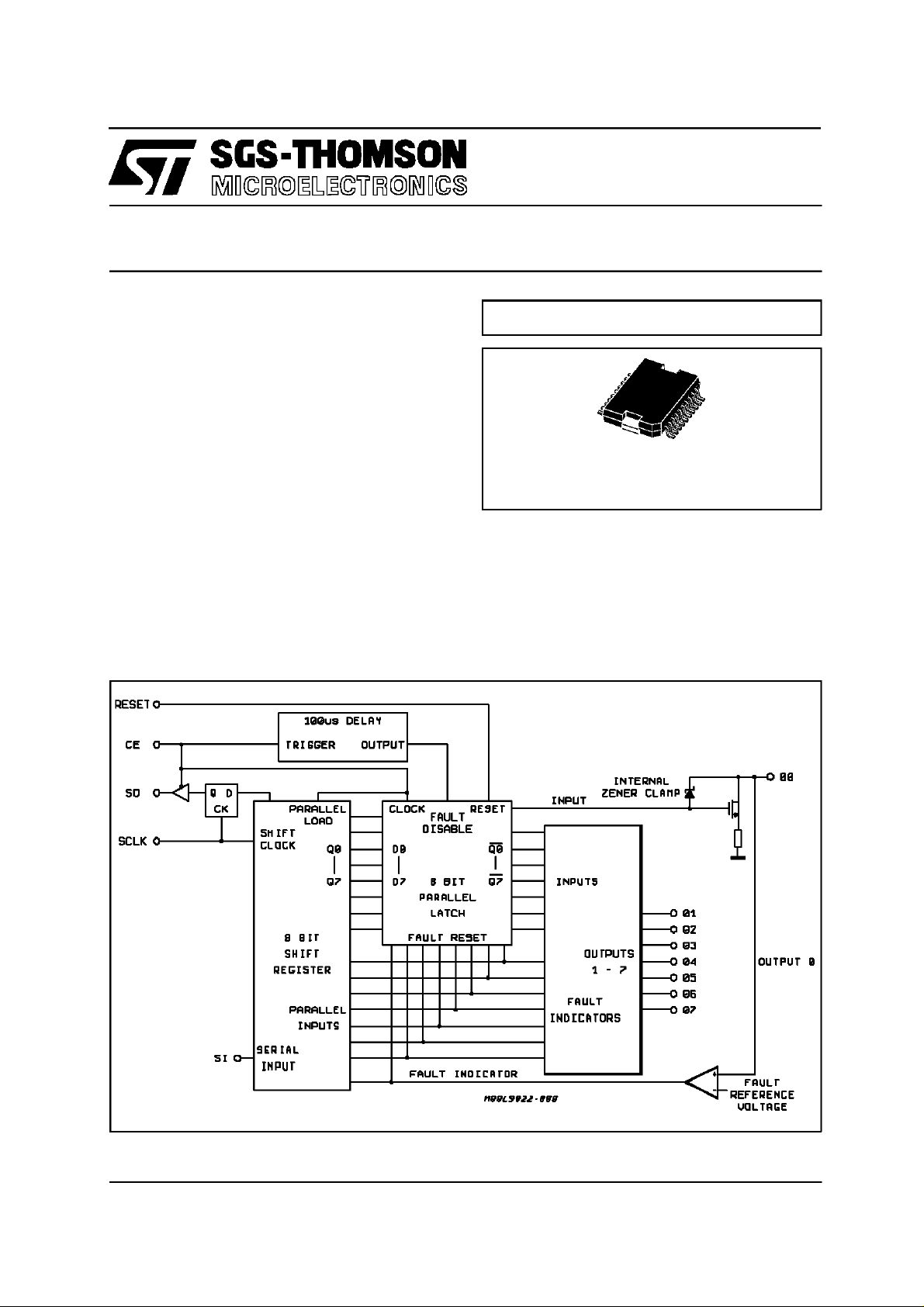
BLOCKDIAGRAM
MULTIPO WER BCD TECHNOLOG Y
PowerSO20
ORDERINGNUMBER: L9822N
tomotive environment. The DMOS outpts L9822N
has a verylow power consumption.
Data is transmitted serially to the device usingthe
SerialPeripheralInterface(SPI)protocol.
The L9822Nfeaturestheoutputsstatusmonitoring
function.
October1997
1/9

L9822N
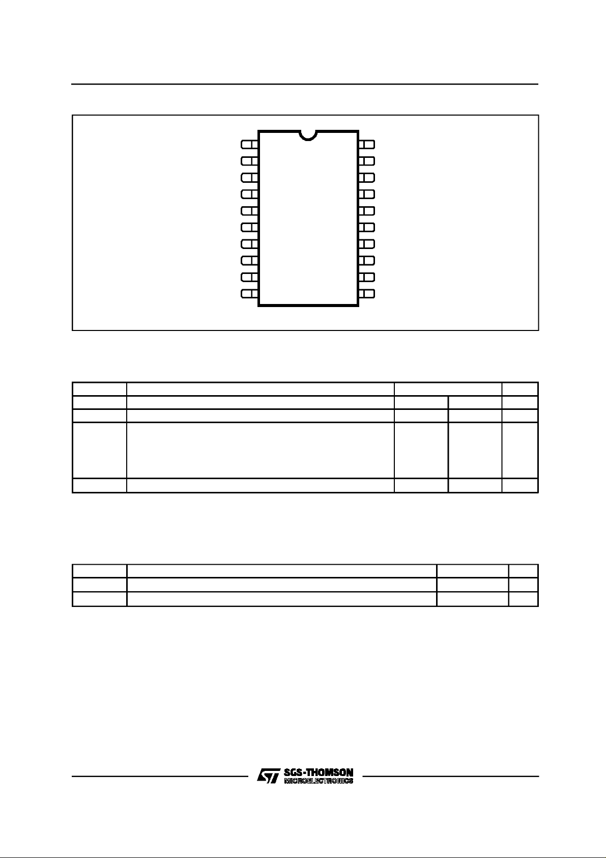
PIN CONNECTIONS
(topview)
RESET
GND
2
3
V
SO
CC
4
OUT7
OUT6
OUT5
OUT4
N.C. N.C.
GND GND
5
6
7
8
9
10
D94AT119A
20
19
18
17
16
15
14
13
12
11
GND1
SI
SCLK
CE
OUT0
OUT1
OUT2
OUT3
ABSOLUTEMAXIMUM RATINGS
Symbol Parameter Value Unit
DC Logic Supply – 0.7 7 V
Output Voltage – 0.7 40 V
Input Transient Current
(CE, SI, SCLK, RESET, SO) :
Duration Time t = 1s,
<0
V
I
V
I>VCC
Junction and Storage Temperature Range – 40 150
stg
–25
+25
T
j
V
CC
V
O
I
I
,T
mA
mA
°
C
THERMAL DATA
Symbol Parameter Value Unit
Thermal Resistance Junction-Case Max. 1.5
Thermal Resistance Junction-Ambient Max. 60
2/9
R
th j-case
R
th j-amb
C/W
°
C/W
°

PIN DESCRIPTION
L9822N
V
CC
Logicsupplyvoltage - nominally 5V
GROUND
DeviceGround.Thisgroundappliesforthelogiccircuitsas well as the poweroutputstages.
RESET
Asynchronousresetfortheoutputstages,theparal-
lellatchand the shiftregisterinsidetheL9822NSP.
Thispin isactivelowandit mustnotbe left floating.
Apoweronclearfunctionmaybe implementedconnectingthis pin to V
withan externalresistorand
CC
to groundwith an externalcapacitor.
CE
ChipEnable. Datais transferredfromthe shift registerstotheoutputson the risingedgeof thissignal.
Thefalling edgeof this signalsets the shiftregister
with the outputvoltagesensebits coming from the
output stages.The output driver for the SO pin is
enabledwhen this pinis low.
SO
SerialOutput.This pin is theserialoutputfrom the
shift register andit is tri-stated when CE is high.A
highfor a data biton thispin indicatesthat the par-
ticularoutput is high. A low on thispin for adatabit
indicatesthat the outputis low.
Comparing the serial output bits with the previous
serial input bits the external microcontroller implementsthediagnosticdata supplied by theL9822.
SI
SerialInput.Thispin is theserialdata input.A high
onthispinwillprogramaparticularoutputtobeOFF,
whilea lowwill turn itON.
SCLK
SerialClock.This pin clocksthe shift register.New
SO data will appearon every rising edgeof thispin
andnewSIdatawillbe latchedoneverySCLK’sfallingedgeinto theshiftregister.
OUTPUTS00-07
Poweroutputpins.The inputandoutputbitscorres-
pondingto07 aresentandreceivedfirstviatheSPI
bus and 00is thelast.
The outputs are provided with current limiting and
voltagesensefunctionsfor fault indicationand protection.The nominal load current for theseoutputs
is 500mA. Theoutputsalsohave on boardclamps
set at about 36V for recirculation of inductiveload
current.
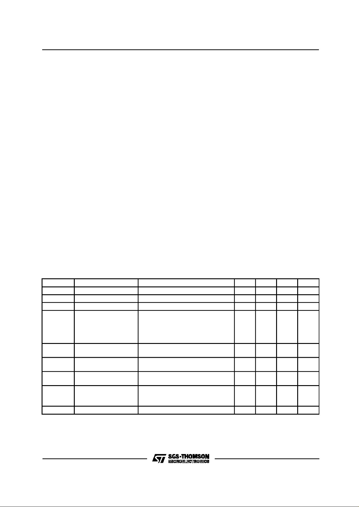
ELECTRICALCHARACTERISTICS (V
Symbol Parameter Test Conditions Min. Typ. Max. Unit
Output Clamping Volt. IO= 0.5A, Output Programmed OFF 30 35 40 V
Out. Clamping Energy IO= 0.5A, When ON 20 mJ
Out. Leakage Current VO= 24V, Output Progr. OFF 1 mA
On Resistance Output Progr. ON
Turn-on Delay IO= 500mA
Turn-off Delay IO= 500mA
Fault Refer. Voltage Output Progr. OFF
Fault Reset Delay
(after CE L to H
transition)
Output OFF Voltage Output Pin Floating.cOutput Progr. OFF, 1.0 V
R
V
V
V
OC
E
OC
I
OFF
DSon
t
PHL
t
P
OREF
t
UD
OFF
=5V±5%.Tj=– 40to 125°C ; unlessotherwise speciifed)
CC
= 0.5A
I
O
= 0.75A
I
O
=1A
I
O
With Fault Reset Disabled
No Reactive Load
No Reactive Load
1.6 2 V
Fault detected if V
See fig. 3 75 250
O>VOREF
0.53
0.53
0.53
1
1
1
10
10
Ω
Ω
Ω
s
µ
s
µ
s
µ
3/9
 Loading...