

L9822E
OCTALSERIAL SOLENOID DRIVER
ADVAN CE D AT A
. EIGHT LOWR
(0.5ΩATI
=1A@25°CVCC=5V±5%)
O
DMOSOUTPUTS
DSon
.8 BITSERIAL INPUTDATA (SPI)
.
8 BIT SERIAL DIAGNOSTIC OUTPUT FOR
OVERLOADANDOPENCIRCUITCONDITIONS
.OUTPUT SHORT CIRCUITPROTECTION
.CHIPENABLESELECTFUNCTION(activelow)
.INTERNAL 36V CLAMPINGFOR EACH OUT-
PUT
.CASCADABLE WITH ANOTHER OCTAL
DRIVER
.LOWQUIESCENTCURRENT (10mAMAX.)
.
PACKAGE MULTIWATT15, PowerSO20 AND
SO20L
DESCRIPTION
TheL9822E is an octal low side solenoiddriver
realized in Multipower-BCDtechnologyparticularly
suitedfor drivinglamps,relaysand solenoidsin au-
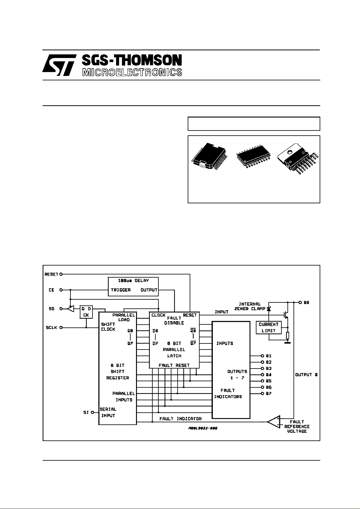
BLOCKDIAGRAM
MULTIPO WER BCD TECHNOLOG Y
PowerSO20 SO20L(16+2+2) Multiwatt15
ORDERINGNUMBERS: L9822E (Multiwatt15)
L9822EPD (PowerSO20)
L9822ED(SO20L )
tomotive environment. The DMOS outpts L9822E
has a verylow power consumption.
Data is transmitted serially to the device usingthe
SerialPeripheralInterface(SPI)protocol.
The L9822Efeaturesthe outputsstatusmonitoring
function.
September 1994
This is advanced informationon a new product now in development or undergoingevaluation. Detailsare subject to change withoutnotice.
1/11
L9822E
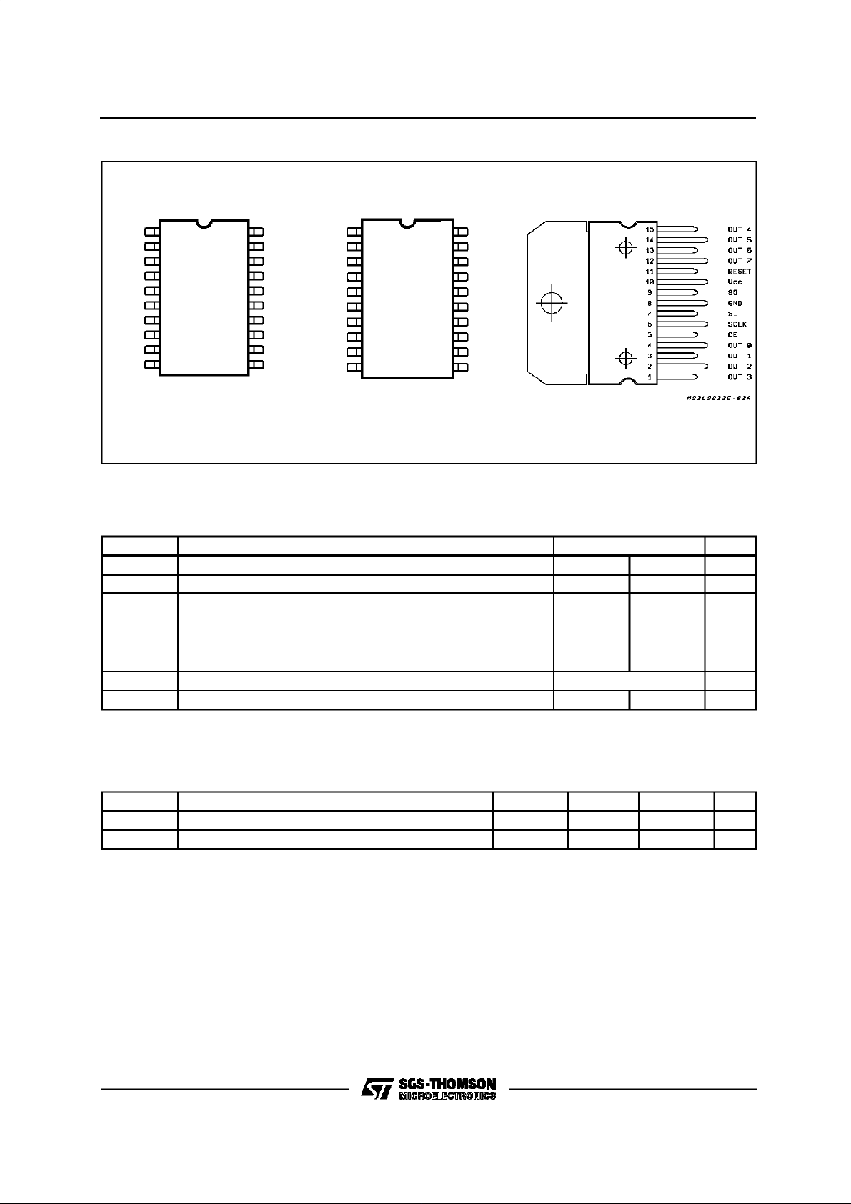
PIN CONNECTIONS(topview)
GND
SO
2
V
RESET
OUT7
OUT6
OUT5
OUT4
N.C. N.C.
GND GND
3
DD
4
5
6
7
8
9
10
D94AT119
PowerSO20 Multiwatt15
GND1
20
SI
19
SCLK
18
CE
17
OUT0
16
OUT1
15
OUT2
14
OUT3
13
12
11
OUT6
OUT5
OUT4
N.C.
GND
GND
N.C.
OUT3
OUT2 CE
OUT1 OUT0
2
3
4
5
6
7
8
9
10
D94AT118
OUT71
20
RESET
19
V
18
17
16
15
14
13
12
11
DD
SO
GND
GND
SI
SLCK
SO20L
ABSOLUTEMAXIMUM RATINGS
Symbol Parameter Value Unit
DC Logic Supply – 0.7 7 V
Output Voltage – 0.7 40 V
Input Transient Current
(CE, SI, SCLK, RESET, SO) :
Duration Time t = 1s,
VI<0
V
I>VCC
–25
Continous Output Current (for each output) Int. Limited A
Junction and Storage Temperature Range – 40 150
stg
+25
T
j
V
CC
V
O
I
I
I
Odc
,T
mA
mA
°
C
THERMAL DATA
Symbol Parameter Multiwatt15 SO20L PowerSO20 Unit
Thermal Resistance Junction-Case Max. 2 25 1.5
Thermal Resistance Junction-Ambient Max. 35 70 60
2/11
R
th j-case
R
th j-amb
C/W
°
C/W
°
PIN DESCRIPTION
L98 22E
V
CC
Logicsupplyvoltage - nominally 5V
GROUND
DeviceGround.Thisgroundappliesforthelogiccircuitsas well as the poweroutputstages.
RESET
Asynchronousresetfortheoutputstages,theparal-
lellatchandthe shiftregisterinsidetheL9822ESP.
Thispin isactivelow and it mustnotbe leftfloating.
Apoweron clearfunctionmaybeimplementedconnectingthis pin to V
withan externalresistorand
CC
to groundwith an externalcapacitor.
CE
ChipEnable.Datais transferredfromthe shift registersto the outputsonthe risingedgeof thissignal.
Thefallingedge of thissignalsetsthe shift register
with the outputvoltagesensebits coming from the
output stages.The output driver for the SO pin is
enabledwhen this pinis low.
SO
SerialOutput.This pin is theserialoutputfrom the
shift register andit is tri-stated when CE is high.A
highfor a data bit on thispin indicatesthatthe par-
ticularoutputis high. A low on thispin for adata bit
indicatesthat the outputis low.
Comparing the serial output bits with the previous
serial input bits the external microcontroller implementsthediagnosticdata supplied by theL9822.
SI
SerialInput.Thispin is theserialdata input.A high
onthispinwillprogramaparticularoutputtobeOFF,
whilea lowwill turn itON.
SCLK
SerialClock.This pin clocksthe shift register.New
SO data will appearon every rising edge of thispin
andnewSIdatawillbelatchedoneverySCLK’sfallingedgeinto theshiftregister.
OUTPUTS00-07
Poweroutputpins.Theinputandoutputbitscorres-
pondingto 07 aresentand receivedfirstvia the SPI
busand00is thelast.Theoutputsareprovidedwith
currentlimiting andvoltagesensefunctionsforfault
indicationand protection.Thenominal load current
for theseoutputsis500mA, but thecurrentlimiting
issetto aminimumof1.05A.Theoutputsalsohave
on board clamps set at about 36V for recirculation
of inductiveload current.
ELECTRICALCHARACTERISTICS (V
Symbol Parameter Test Conditions Min. Typ. Max. Unit
Output Clamping Volt. IO= 0.5A, Output Programmed OFF 30 40 V
Out. Clamping Energy IO= 0.5A, When ON 20 mJ
Out. Leakage Current VO= 24V, Output Progr. OFF 1 mA
On Resistance Output Progr. ON
Out. Self Limiting
Current
Turn-on Delay IO= 500mA
Turn-off Delay IO= 500mA
Fault Refer. Voltage Output Progr. OFF
Fault Reset Delay
(after CE L to H
transition)
Output OFF Voltage Output Pin Floating.cOutput Progr. OFF, 1.0 V
I
R
V
V
V
OC
E
OC
Oleak
DSon
I
OL
t
PHL
t
P
OREF
t
UD
OFF
=5V±5%. Tj=– 40to 125°C ; unlessotherwise speciifed)
CC
= 0.5A
I
O
= 0.8A
I
O
=1A
I
O
With Fault Reset Disabled
Output Progr. ON 1.05 A
No Reactive Load
No Reactive Load
1.6 2 V
Fault detected if V
See fig. 3 75 250 µs
O>VOREF
0.55
0.55
0.55
1
1
1
10 µs
10
Ω
Ω
Ω
s
µ
3/11
L9822E
ELECTRICALCHARACTERISTICS (Continued)
Symbol Parameter Test Conditions Min. Typ. Max. Unit
INPUTBUFFER(SI, CE,SCLK andRESETpins)
V
T–
Threshold Voltage at
VCC=5V±10% 0.2V
Falling Edge
SCLK only
V
T+
Threshold Voltage at
VCC=5V±10% 0.7V
Rising Edge
SCLK only
V
C
H
I
I
Hysteresis Voltage VT+–V
T–
Input Current VCC= 5.50V, 0 < VI<V
Input Capacitance 0 < VI<V
I
CC
CC
OUTPUT BUFFER(SOpin)
V
SOL
V
SOH
I
SOtl
C
SO
I
CC
Output LOW Voltage IO= 1.6mA 0.4 V
Output HIGH Voltage IO= 0.8mA V
Output Tristate Leakage
Current
Output Capacitance 0 < VO<V
0<VO<VCC, CE Pin Held High,
= 5.25V
V
CC
CC
CE Pin Held High
Quiescent Supply
Current at V
CC
Pin
All Outputs Progr. ON. I
O
per Output Simultaneously
= 0.5A
SERIALPERIPHERAL INTERFACE (see fig.2, timingdiagram)
f
op
t
lead
t
lag
t
wSCKH
t
wSCKL
t
su
t
H
t
EN
t
DIS
t
V
t
rSO
t
fSO
t
rSI
t
fSI
t
ho
Operating Frequency D.C. 2 MHz
Enable Lead Time 250 ns
Enable Lag Time 250 ns
Clock HIGH Time 200 ns
Clock LOW Time 200 ns
Data Setup Time 75 ns
Data Hold Time 75 ns
Enable Time 250 ns
Disable Time 250 ns
Data Valid Time 100 ns
Rise Time (SO output) VCC= 20 to 70% CL= 200pF 50 ns
Fall Time (SO output) VCC= 70 to 20% CL= 200pF 50 ns
Rise Time SPI
VCC= 20 to 70% CL= 200pF 200 ns
Inputs (SCK, SI, CE)
Fall Time SPI
VCC= 70 to 20% CL= 200pF 200 ns
Inputs (SCLK, SI, CE)
Output Data Hold Time 0
CC
0.6
CC
4.15
0.85 2.5 V
–10 +10
20 nF
CC
– 1.3V
–20 20
20 pF
10 mA
µ
µ
V
V
V
V
A
V
A
s
µ
4/11

FUNCTIONALDESCRIPTION
TheL9822ESPDMOSoutputisa lowoperatingpowerdevicefeatu-ring,eight 1ΩR
DMOSdrivers
DSON
with transient protection circuits in output stages.
Eachchannelis independentlycontrolledby an outputlatchanda commonRESETlinewhichdisables
all eightoutputs.The driver has low saturationand
shortcircuitprotectionandcandriveinductiveandresistive loads such as solenoids, lamps and relais.
DataistransmittedtothedeviceseriallyusingtheSerialPeripheralInterface(SPI)protocol.Thecircuitreceives8 bit serialdata by meansof the serial input
(SI)which is storedinan internalregisterto control
theoutputdrivers.The serialoutput(SO)provides8
bit ofdiagnosticdata representingthe voltage level
at thedriver output.Thisallows themicroprocessor
to diagnosetheconditionof theoutputdrivers.
The output saturation voltage is monitored by a
comparatorfor an outof saturationconditionandis
abletounlatchtheparticulardriverthroughthefault
resetline. Thiscircuitis also cascadablewith another octal driver in order to jam 8 bit multiple data.
The device is selected when the chip enable (CE)
lineis low.
Additionallythe (SO) is placed in a tri-state mode
when the deviceis deselected.The negativeedge
of the(CE) transfersthevoltagelevel of thedrivers
totheshiftregisterand thepositiveedgeof the(CE)
latchesthenewdatafromtheshiftregistertothedrivers. WhenCE is Low, data bit containedinto the
shift register is transferred to SO output at every
SCLKpositivetransitionwhiledatabitpresentat SI
inputis latchedintotheshift registeron everySCLK
negativetransition.
InternalBlocksDescription
The internalarchitectureof the deviceis based on
the threeinternalmajorblocks: theoctalshiftregisterfortalkingtotheSPIbus, the octallatchfor holdingcontrolbits writtenintothedeviceandthe octal
load driverarray.
Shift Register
The shiftregisterhas bothserial and parallelinputs
and serial and parallel outputs.Theserial input acceptsdatafromthe SPIbusand theserial outputsimultaneously sends data into the SPI bus. The
paralleloutputsarelatchedinto the parallellatchinsidetheL9822ESPattheendofadatatransfer.The
parallelinputs jam diagnosticdata intothe shiftregisterat thebeginningof a datatransfercycle.
ParallelLatch
The parallellatchholds the input datafromtheshift
register.This datathen actuatestheoutputstages.
L98 22E
Individualregisters in the latch may be clearedby
fault conditions in order to protectthe overloaded
outputstages.Theentire latchmayalsobecleared
by theRESET signal.
OutputStages
Theoutputstagesprovideanactivelowdrivesignal
suitable for 0.75A continuous loads. Each output
has a currentlimit circuit which limits the maximum
outputcurrentto atleast1.05Ato allowfor high inrushcurrents.Additionally,theoutputshaveinternal
zenersset to 36 voltsto clamp inductivetransients
at turn-off.Each output also has a voltage comparatorobservingtheoutputnode.If thevoltageexceeds 1.8V on an ON output pin, a fault condition is
assumedand the latch drivingthis particular stage
is reset, turningthe outputOFF to protectit. Thetiming of thisactionis describedbelow.These comparators also provide diagnosticfeedback data to
theshiftregister.Additionally,thecomparatorscontainaninternalpulldowncurrentwhichwillcausethe
cell to indicate a low outputvoltageif the outputis
programmedOFF and theoutputpinisopencircuited.
TIMINGDATA TRANSFER
Figure#2 showsthe overalltiming diagramfrom a
byte transferto and from the L9822ESPusing the
SPIbus.
CE Highto LowTransition
TheactionbeginswhentheChip Enable(CE) pinis
pulledlow.Thetri-stateSerialOutput(SO)pindriver
willbeenabledentire timethatCE is low. At the fallingedge of theCEpin,thediagnosticdatafromthe
voltagecomparatorsin theoutputstageswillbelatched into the shift register.If a particularoutput is
high, a logic one will be jammedinto that bit in the
shiftregister.Iftheoutputis low,a logiczerowillbe
loadedthere.Themostsignificantbit(07)shouldbe
presentedat theSerialInput(SI) pin. A zeroat this
pin will programan outputON, whilea onewillprogramthe outputOFF.
SCLK Transitions
The Serial Clock(SCLK) pinshould then be pulled
high.At thispointthediagnosticbitfromthe mostsignificantoutput(07)willappearat theSOpin.Ahigh
here indicates that the 07 pin is higher than 1.8V.
TheSCLKpinshouldthenbetoggledlowthenhigh.
NewSOdatawillappearfollowingeveryrisingedge
of SCLK and new SI data will be latched into the
L9822ESPshiftregisteronthefallingedges.Anunlimited amount of data may be shiftedthrough the
5/11

L9822E
deviceshiftregister(into theSI pin and out the SO
pin),allowingthe otherSPI devicestobecascaded
in a daisychainwiththe L9822ESP.
CELow to HighTransition
Once the last data bit has been shifted into the
L9822ESP,the CE pin shouldbe pulled high.
Attherisingedge of CE the shiftregisterdata is latchedintotheparallellatchandtheoutputstageswill
beactuatedbythe new data.Aninternal160µsdelaytimerwillalso be started at thisrisingedge(see
). During the 160µs period, the outputs will be
t
UD
protectedonlyby the analog currentlimitingcircuits
since the resetting of the parallel latches by faults
conditionswillbeinhibitedduringthisperiod.Thisallowsthe part toovercomeany highinrushcurrents
that may flow immediately after turn on. Once the
delay period has elapsed, the output voltages are
sensedbythe comparatorsand anyoutputwithvoltageshigherthan1.8VarelatchedOFF.Itshouldbe
notedthat the SCLK pin shouldbe low at both tran-
Figure 1
: Byte Timing with AsynchronousReset.
sitionsof the CE pin to avoid any false clocking of
theshiftregister.TheSCLKinputisgatedby theCE
pin, so that the SCLK pin is ignored whenever the
CE pinis high.
FAULTCONDITIONSCHECK
Checkingforfaultconditionsmaybedonein thefol-
lowing way. Clock in a new controlbyte. Wait 160
microseconds or so to allow the outputsto settle.
Clockinthesamecontrolbyteandobservethediagnosticdata that comes outof the device.The diagnostic bits should beidentical to the bits that were
firstclockedin.Anydifferenceswouldpointtoafault
onthatoutput.If theoutputwasprogrammedONby
clockingin a zero,anda one camebackas thediagnosticbitforthatoutput,the outputpinwasstillhigh
anda shortcircuit oroverloadconditionexists.Ifthe
output was programmedOFF byclocking in a one,
and a zerocameback asthe diagnosticbitfor that
output,nothinghad pulledtheoutputpin highandit
6/11

Figure 2 : TimingDiagram.
L98 22E
Figure 3 : TypicalApplication Circuit.
7/11

L9822E
MULTIWATT15 PACKAGE MECHANICAL DATA
DIM.
A 5 0.197
B 2.65 0.104
C 1.6 0.063
D 1 0.039
E 0.49 0.55 0.019 0.022
F 0.66 0.75 0.026 0.030
G 1.02 1.27 1.52 0.040 0.050 0.060
G1 17.53 17.78 18.03 0.690 0.700 0.710
H1 19.6 0.772
H2 20.2 0.795
L 21.9 22.2 22.5 0.862 0.874 0.886
L1 21.7 22.1 22.5 0.854 0.870 0.886
L2 17.65 18.1 0.695 0.713
L3 17.25 17.5 17.75 0.679 0.689 0.699
L4 10.3 10.7 10.9 0.406 0.421 0.429
L7 2.65 2.9 0.104 0.114
M 4.25 4.55 4.85 0.167 0.179 0.191
M1 4.63 5.08 5.53 0.182 0.200 0.218
S 1.9 2.6 0.075 0.102
S1 1.9 2.6 0.075 0.102
Dia1 3.65 3.85 0.144 0.152
MIN. TYP. MAX. MIN. TYP. MAX.
mm inch
8/11

PowerSO20 PACKAGE MECHANICAL DATA
L98 22E
DIM.
mm inch
MIN. TYP. MAX. MIN. TYP. MAX.
A 3.60 0.1417
a1 0.10 0.30 0.0039 0.0118
a2 3.30 0.1299
a3 0 0.10 0 0.0039
b 0.40 0.53 0.0157 0.0209
c 0.23 0.32 0.009 0.0126
D (1) 15.80 16.00 0.6220 0.6299
E 13.90 14.50 0.5472 0.570
e 1.27 0.050
e3 11.43 0.450
E1 (1) 10.90 11.10 0.4291 0.437
E2 2.90 0.1141
G 0 0.10 0 0.0039
h 1.10 0.0433
L 0.80 1.10 0.0314 0.0433
N10°(max.)
S8
(max.)
°
T 10.0 0.3937
(1) ”D and F” do not include mold flash or protrusions
- Mold flash or protrusions shall not exceed 0.15mm (0.006”)
E2
hx45°
NN
a2
A
b
DETAILA
e3
e
DETAILB
R
D
1120
E1
T
110
PSO20MEC
lead
a3
Gage Plane
E
DETAILB
0.35
S
a1
L
c
DETAILA
slug
-C-
SEATING PLANE
GC
(COPLANARITY)
9/11

L9822E
SO20 PACKAGE MECHANICAL DATA
DIM.
MIN TYP MAX MIN TYP MAX
A 2.65 0.104
a1 0.1 0.2 0.004 0.008
a2 2.45 0.096
b 0.35 0.49 0.014 0.019
b1 0.23 0.32 0.009 0.013
C 0.5 0.020
c1 45° (typ.)
D 1 12.6 0.039 0.496
E 10 10.65 0.394 0.419
e 1.27 0.050
e3 11.43 0.450
F 1 7.4 0.039 0.291
G 8.8 9.15 0.346 0.360
L 0.5 1.27 0.020 0.050
M 0.75 0.030
mm inch
S8°(max.)
10/11

L98 22E
Information furnished is believed to be accurate and reliable. However, SGS-THOMSON Microelectronics assumes no responsibility for
the consequences of use of such information nor for any infringement of patents or other rights of third parties which may result from its
use. No license is granted by implication or otherwise under any patent or patent rights of SGS-THOMSON Microelectronics. Specification
mentioned in this publication are subject to change without notice. This publication supersedes and replaces all information previously
supplied. SGS-THOMSON Microelectronics products are not authorized for use as critical components in life support devices or systems
withoutexpress written approval of SGS-THOMSON Microelectronics.
1996 SGS-THOMSON Microelectronics – Printed in Italy – All Rights Reserved
MULTIWATT is a Registered Trademark of SGS-THOMSON Microelectronics
PowerSO-20 is a Trademark of SGS-THOMSON Microelectronics
Australia - Brazil - Canada - China - France - Germany - Hong Kong - Italy - Japan - Korea - Malaysia - Malta - Morocco -
The Netherlands - Singapore - Spain - Sweden - Switzerland - Taiwan - Thailand - United Kingdom - U.S.A.
SGS-THOMSON Microelectronics GROUP OF COMPANIES
11/11
 Loading...