

L9822E
OCTALSERIAL SOLENOID DRIVER
ADVAN CE D AT A
. EIGHT LOWR
(0.5ΩATI
=1A@25°CVCC=5V±5%)
O
DMOSOUTPUTS
DSon
.8 BITSERIAL INPUTDATA (SPI)
.
8 BIT SERIAL DIAGNOSTIC OUTPUT FOR
OVERLOADANDOPENCIRCUITCONDITIONS
.OUTPUT SHORT CIRCUITPROTECTION
.CHIPENABLESELECTFUNCTION(activelow)
.INTERNAL 36V CLAMPINGFOR EACH OUT-
PUT
.CASCADABLE WITH ANOTHER OCTAL
DRIVER
.LOWQUIESCENTCURRENT (10mAMAX.)
.
PACKAGE MULTIWATT15, PowerSO20 AND
SO20L
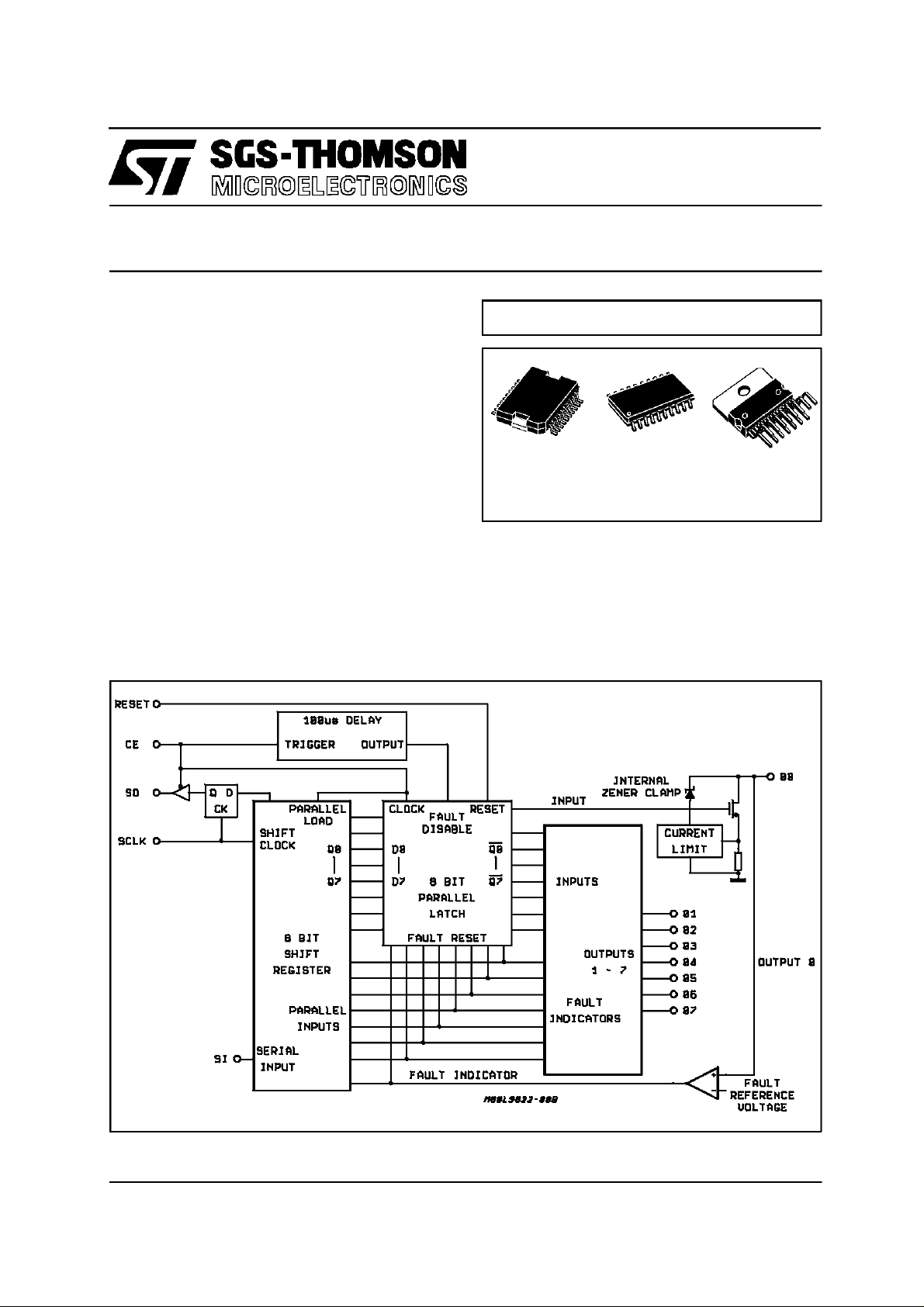
DESCRIPTION
TheL9822E is an octal low side solenoiddriver
realized in Multipower-BCDtechnologyparticularly
suitedfor drivinglamps,relaysand solenoidsin au-
BLOCKDIAGRAM
MULTIPO WER BCD TECHNOLOG Y
PowerSO20 SO20L(16+2+2) Multiwatt15
ORDERINGNUMBERS: L9822E (Multiwatt15)
L9822EPD (PowerSO20)
L9822ED(SO20L )
tomotive environment. The DMOS outpts L9822E
has a verylow power consumption.
Data is transmitted serially to the device usingthe
SerialPeripheralInterface(SPI)protocol.
The L9822Efeaturesthe outputsstatusmonitoring
function.
September 1994
This is advanced informationon a new product now in development or undergoingevaluation. Detailsare subject to change withoutnotice.
1/11
L9822E
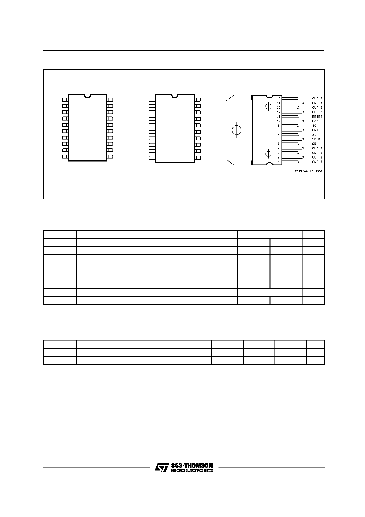
PIN CONNECTIONS(topview)
GND
SO
2
V
RESET
OUT7
OUT6
OUT5
OUT4
N.C. N.C.
GND GND
3
DD
4
5
6
7
8
9
10
D94AT119
PowerSO20 Multiwatt15
GND1
20
SI
19
SCLK
18
CE
17
OUT0
16
OUT1
15
OUT2
14
OUT3
13
12
11
OUT6
OUT5
OUT4
N.C.
GND
GND
N.C.
OUT3
OUT2 CE
OUT1 OUT0
2
3
4
5
6
7
8
9
10
D94AT118
OUT71
20
RESET
19
V
18
17
16
15
14
13
12
11
DD
SO
GND
GND
SI
SLCK
SO20L
ABSOLUTEMAXIMUM RATINGS
Symbol Parameter Value Unit
DC Logic Supply – 0.7 7 V
Output Voltage – 0.7 40 V
Input Transient Current
(CE, SI, SCLK, RESET, SO) :
Duration Time t = 1s,
VI<0
V
I>VCC
–25
Continous Output Current (for each output) Int. Limited A
Junction and Storage Temperature Range – 40 150
stg
+25
T
j
V
CC
V
O
I
I
I
Odc
,T
mA
mA
°
C
THERMAL DATA
Symbol Parameter Multiwatt15 SO20L PowerSO20 Unit
Thermal Resistance Junction-Case Max. 2 25 1.5
Thermal Resistance Junction-Ambient Max. 35 70 60
2/11
R
th j-case
R
th j-amb
C/W
°
C/W
°
PIN DESCRIPTION
L98 22E
V
CC
Logicsupplyvoltage - nominally 5V
GROUND
DeviceGround.Thisgroundappliesforthelogiccircuitsas well as the poweroutputstages.
RESET
Asynchronousresetfortheoutputstages,theparal-
lellatchandthe shiftregisterinsidetheL9822ESP.
Thispin isactivelow and it mustnotbe leftfloating.
Apoweron clearfunctionmaybeimplementedconnectingthis pin to V
withan externalresistorand
CC
to groundwith an externalcapacitor.
CE
ChipEnable.Datais transferredfromthe shift registersto the outputsonthe risingedgeof thissignal.
Thefallingedge of thissignalsetsthe shift register
with the outputvoltagesensebits coming from the
output stages.The output driver for the SO pin is
enabledwhen this pinis low.
SO
SerialOutput.This pin is theserialoutputfrom the
shift register andit is tri-stated when CE is high.A
highfor a data bit on thispin indicatesthatthe par-
ticularoutputis high. A low on thispin for adata bit
indicatesthat the outputis low.
Comparing the serial output bits with the previous
serial input bits the external microcontroller implementsthediagnosticdata supplied by theL9822.
SI
SerialInput.Thispin is theserialdata input.A high
onthispinwillprogramaparticularoutputtobeOFF,
whilea lowwill turn itON.
SCLK
SerialClock.This pin clocksthe shift register.New
SO data will appearon every rising edge of thispin
andnewSIdatawillbelatchedoneverySCLK’sfallingedgeinto theshiftregister.
OUTPUTS00-07
Poweroutputpins.Theinputandoutputbitscorres-
pondingto 07 aresentand receivedfirstvia the SPI
busand00is thelast.Theoutputsareprovidedwith
currentlimiting andvoltagesensefunctionsforfault
indicationand protection.Thenominal load current
for theseoutputsis500mA, but thecurrentlimiting
issetto aminimumof1.05A.Theoutputsalsohave
on board clamps set at about 36V for recirculation
of inductiveload current.
ELECTRICALCHARACTERISTICS (V
Symbol Parameter Test Conditions Min. Typ. Max. Unit
Output Clamping Volt. IO= 0.5A, Output Programmed OFF 30 40 V
Out. Clamping Energy IO= 0.5A, When ON 20 mJ
Out. Leakage Current VO= 24V, Output Progr. OFF 1 mA
On Resistance Output Progr. ON
Out. Self Limiting
Current
Turn-on Delay IO= 500mA
Turn-off Delay IO= 500mA
Fault Refer. Voltage Output Progr. OFF
Fault Reset Delay
(after CE L to H
transition)
Output OFF Voltage Output Pin Floating.cOutput Progr. OFF, 1.0 V
I
R
V
V
V
OC
E
OC
Oleak
DSon
I
OL
t
PHL
t
P
OREF
t
UD
OFF
=5V±5%. Tj=– 40to 125°C ; unlessotherwise speciifed)
CC
= 0.5A
I
O
= 0.8A
I
O
=1A
I
O
With Fault Reset Disabled
Output Progr. ON 1.05 A
No Reactive Load
No Reactive Load
1.6 2 V
Fault detected if V
See fig. 3 75 250 µs
O>VOREF
0.55
0.55
0.55
1
1
1
10 µs
10
Ω
Ω
Ω
s
µ
3/11
L9822E
ELECTRICALCHARACTERISTICS (Continued)
Symbol Parameter Test Conditions Min. Typ. Max. Unit
INPUTBUFFER(SI, CE,SCLK andRESETpins)
V
T–
Threshold Voltage at
VCC=5V±10% 0.2V
Falling Edge
SCLK only
V
T+
Threshold Voltage at
VCC=5V±10% 0.7V
Rising Edge
SCLK only
V
C
H
I
I
Hysteresis Voltage VT+–V
T–
Input Current VCC= 5.50V, 0 < VI<V
Input Capacitance 0 < VI<V
I
CC
CC
OUTPUT BUFFER(SOpin)
V
SOL
V
SOH
I
SOtl
C
SO
I
CC
Output LOW Voltage IO= 1.6mA 0.4 V
Output HIGH Voltage IO= 0.8mA V
Output Tristate Leakage
Current
Output Capacitance 0 < VO<V
0<VO<VCC, CE Pin Held High,
= 5.25V
V
CC
CC
CE Pin Held High
Quiescent Supply
Current at V
CC
Pin
All Outputs Progr. ON. I
O
per Output Simultaneously
= 0.5A
SERIALPERIPHERAL INTERFACE (see fig.2, timingdiagram)
f
op
t
lead
t
lag
t
wSCKH
t
wSCKL
t
su
t
H
t
EN
t
DIS
t
V
t
rSO
t
fSO
t
rSI
t
fSI
t
ho
Operating Frequency D.C. 2 MHz
Enable Lead Time 250 ns
Enable Lag Time 250 ns
Clock HIGH Time 200 ns
Clock LOW Time 200 ns
Data Setup Time 75 ns
Data Hold Time 75 ns
Enable Time 250 ns
Disable Time 250 ns
Data Valid Time 100 ns
Rise Time (SO output) VCC= 20 to 70% CL= 200pF 50 ns
Fall Time (SO output) VCC= 70 to 20% CL= 200pF 50 ns
Rise Time SPI
VCC= 20 to 70% CL= 200pF 200 ns
Inputs (SCK, SI, CE)
Fall Time SPI
VCC= 70 to 20% CL= 200pF 200 ns
Inputs (SCLK, SI, CE)
Output Data Hold Time 0
CC
0.6
CC
4.15
0.85 2.5 V
–10 +10
20 nF
CC
– 1.3V
–20 20
20 pF
10 mA
µ
µ
V
V
V
V
A
V
A
s
µ
4/11
 Loading...