

.25APEAKOUTPUTCURRENT
.R
= 100mΩ
ON
.DIAGNOSTICAND PROTECTION
FUNCTIONS
.µP COMPATIBLE
.
GROUNDEDCASE
.INRUSHCURRENTLIMITINGCIRCUIT
DES CRIPTION
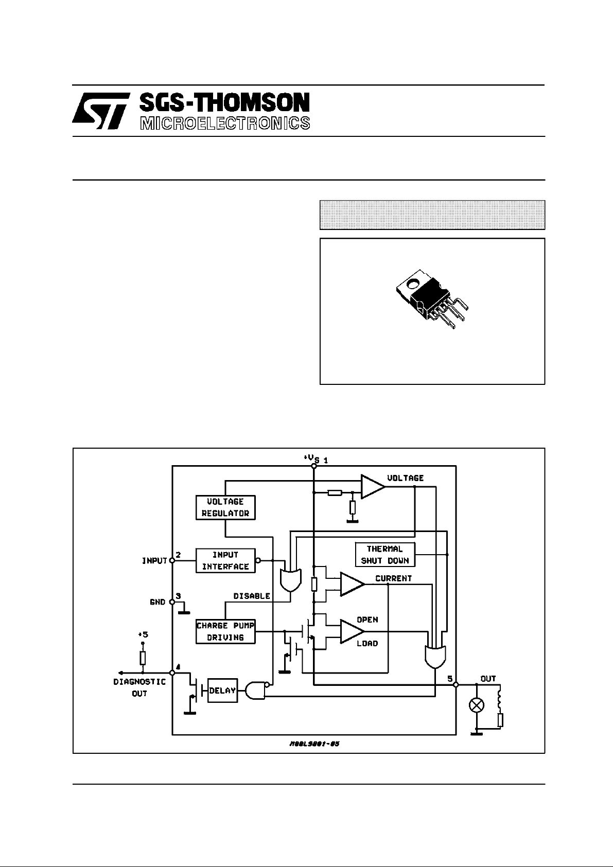
The L9821 High Side Driver realized with Multipower - BCD mixed technology,drivesresistiveor inductiveloadswith one side connectedtoground.
The inputcontrolis TTLcompatibleanda diagnostic outputprovidesan indicationof load (open and
short) and device status (thermal and overvoltage
shutdown).Onchipthermalprotectionandshortcircuitprotectionare provided.
L9821
HIGH SIDE DRIVER
MULTIPOWER BCD TECHNOLOGY
Pentawatt
ORDERING NUMBER : L9821
Thedeviceis assembledinthePentawattpackage
withthe tab connectedtothe groundterminal.
BLOCK DIAGRAM
February 1997
1/7
L9821
ABSOLUTE MAXIMUM RATINGS
Symbol Parameter Value
Max Forward Voltage
V
S
Positive Transient Peak Voltage (dump :
5ms ≤ t
≤ 10ms, R
rise
source
≥ 0.5Ω)
– Resistive Load
– Inductive Load
Reverse Input Voltage – 0.3Vdc
Input Voltage Pin 2 (to GND)
V
I
V
Pin 4 Voltage
4
V
Pin 5 Voltage
5
(to GND)
(to GND)
Pin 1 Current
I
1
I
Pin 2 Current (forced)
2
I
Pin 4 Current (sink)
4
I
Pin 5 Current
5
Power Dissipation Internally Limited
TOT
Junction and Storage Temperature Range – 55°C to + 150°C
STG
T
P
,T
J
*due to the negativevoltage at the output during the switchingoff.
fall time constant = 100ms,
τ
f
– 0.3V / + Vs(Vs< 20V)
– 0.3V / + V
–3V/+V
50Vdc
50V (*)
Internally Limited
0.5mA
10mA
Internally Limited
60V
s(Vs
s(Vs
< 20V)
< 20V)
THERMAL DATA
Symbol Parameter Value Unit
R
th j-case
Thermal Resistance Junction-case Max 1.5 °C/W
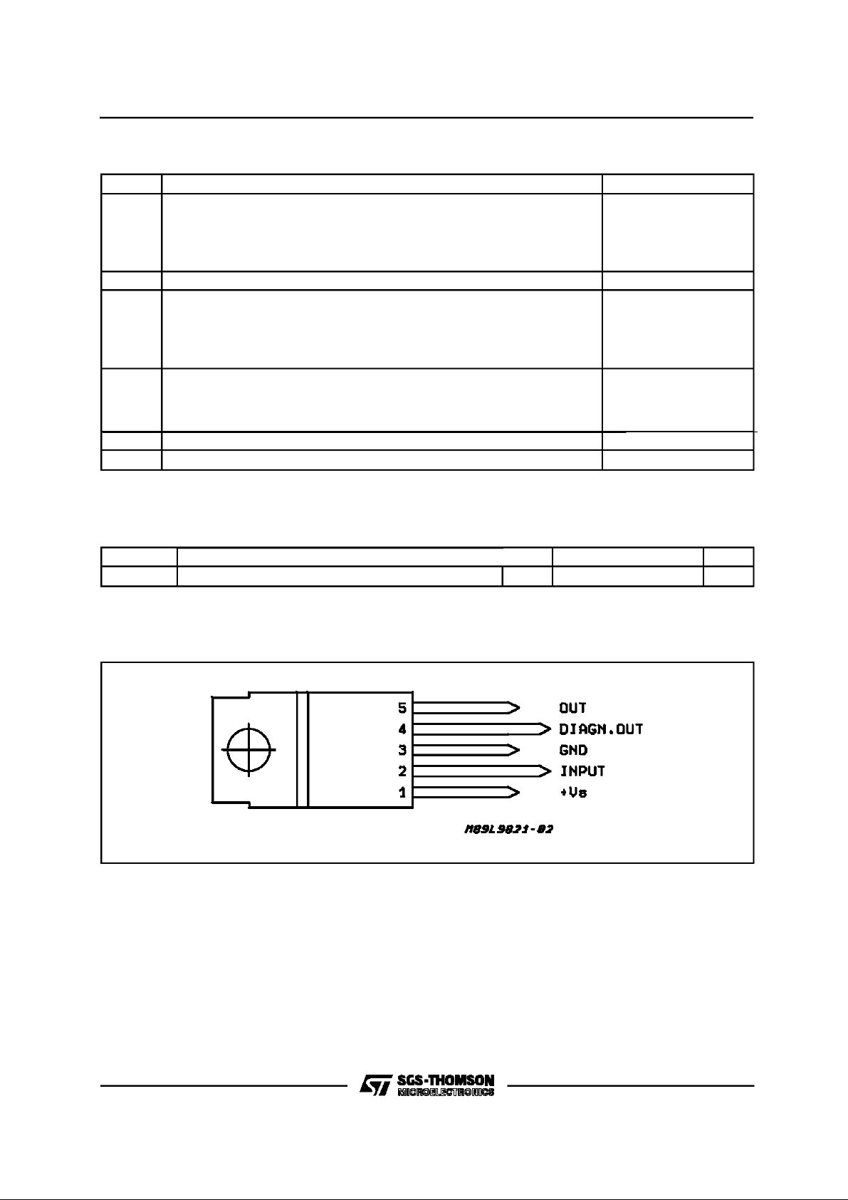
PIN CONNECTI ON (top view)
2/7

PI N FU NCTIO NS
L9821
1. POWERSUPPLY
Supplyvoltageinput.Whenthe supply reachesthe
maximumoperatingvoltage(32V)the deviceis turned off, protectingitself and the load.
Turningoff guaranteedfor V
> 41V.
S
2. INPUT
TTL compatibleinput. High level on thispin means
outputcurrentON.Thelowlevelvoltageswitchesoff
the chargepump, thepower stage and the diagnosticoutputreducingto the minimumvaluethe quiescent current.
condition.Thisoutputdetects with Tipically45ms
delayat T
Overvoltagecondition.
-
Thermalshutdown.
-
Shortcircuit.Thepowerstagecurrentisinternally
-
limitedat 25A.
Open load. The open load conditionis detected
-
withload current< 0.6A.
=25°C thefollowing faults:
amb
The diagnosticoutput is active low. Thediagnostic
delay timeallowsto avoidspuriousdiagnosys(i.e :
turnON overcurrent,overvoltage spikesetc.).
3. GROUND
This pin must be connectedtoground.
4. DIAGNOSTICFEEDBACK
5. POWEROUTPUT
The device is provided with short circuit protection
at Vs ≤ 14.4V
The diagnosticcircuitis active in input high level
ELECTRICAL CHARACTERISTICS (V
Symbol Parameter Test Condition Min. Typ. Max. Unit
V
OP
R
ON
I
SC
I
DL
I
OPD
V
clamp
I
Off
I
ON
V
IL
V
IH
I
I
I
LEAKD
V
SATD
T
Dd
t
dON
t
r
t
dOFF
t
f
Operat. Voltage 6 32 V
On Resistance Input >2V:Tj=25°C
Short circuit current 25 A
Over Current Detection Level 20 A
Open Load Detection Level Device ON 1.2 A
Output Under Voltage Clamping I
Off State Supply Current Tj= -40 to 35°C
ON State Supply Current Tj=25°C10mA
Input Low Level 0.8 V
Input High Level 2.0 V
Input Current Vi=V
Diagnostic Output Leakage
Voltage
Diagnostic Output Saturation
Voltage
Diagnostic Delay Time Tj=25°C; 45 ms
Output ON Delay Time Tj=25°C15µs
Output ON Rise Time Tj=25°C65µs
Output OFF Delay Time Tj=25°C50
Output OFF Fall Time Tj=25°C 100
= 14.4V; -40°C ≤ Tj≤ 125°C,unless otherwise specified)
S
0.1
Input >2V:Full T range
<6A Inductive -12 -4 V
load
=35to85°C
T
j
threshold
VCC = 5V
Diagnostic Output
I
<1.6mA 0.4 V
sink
0.2
100
300
15
10 µA
Ω
µA
A
µ
A
µ
s
µ
s
µ
3/7
 Loading...