

July 2001 1/103
This is preliminary information on a new product now in development. Details are subject to change without notice.
L9805
Super Smart Power Motor Driver with 8-BIT MCU, CAN Interface, 16K EPROM, 256Bytes RAM,
128 Bytes EEPROM, 10 Bit ADC, WDG , 2 Timers , 2 PWM M odu les, Full H-Bridge Driv er
PROUCT PREVIEW
■
6.4-18V Supply Operating Range
■
16 MHz Maximum Oscillator Frequency
■
8 MHz Maximum Internal Clock Frequency
■
Oscillator Supervisor
■
Fully Static operation
■
-40°C to + 150°C Temperature Range
■
User EPROM/OTP: 16 Kbytes
■
Data RAM: 256 bytes
■
Data EEPROM: 128 bytes
■
64 pin HiQUAD64 package
■
10 multifunctional bidirectional I/O lines
■
Two 16-bit Timers, each featuring:
– 2 Input Captures
– 2 Output Compares
– External Clock input (on Timer 1)
– PWM and Pulse Generator modes
■
Two Programmable 16-bit PWM generator
modules.
■
CAN peripheral including Bus line interface
according 2A/B passive specifications
■
10-bit Analog-to-Digital Converter
■
Software Watchdog for system integrity
■
Master Reset, Power-On Reset, Low Voltage
Reset
■
70mΩ DMOS H-bridge.
■
8-bit Data Manipulation
■
63 basic Instructions and 17 main Addressing
Modes
■
8 x 8 Unsigned Multiply Instruction
■
True Bit Manipulation
■
Complete Development Support on DOS/
WINDOWS
TM
Real-Time Emulator
■
Full Software Package on DOS/WINDOWS
TM
(C-Compiler, Cross-Assembler, Debugger)
HiQUAD-64
ORDERING NUMBER: L9805
1

2/103
Table of Contents
103
L9805
1 GENERAL DESCRIPTION . . . . . . . . . . . . . . . . . . . . . . . . . . . . . . . . . . . . . . . . . . . . . . . . . . . . . . 5
1.1 INTRODUCTION . . . . . . . . . . . . . . . . . . . . . . . . . . . . . . . . . . . . . . . . . . . . . . . . . . . . . . . . . 5
1.2 OTP, ROM AND EPROM DEVICES . . . . . . . . . . . . . . . . . . . . . . . . . . . . . . . . . . . . . . . . . . 5
1.3 PIN OUT. . . . . . . . . . . . . . . . . . . . . . . . . . . . . . . . . . . . . . . . . . . . . . . . . . . . . . . . . . . . . . . . 7
1.4 PIN DESCRIPTION . . . . . . . . . . . . . . . . . . . . . . . . . . . . . . . . . . . . . . . . . . . . . . . . . . . . . . . 8
1.5 REGISTER & MEMORY MAP . . . . . . . . . . . . . . . . . . . . . . . . . . . . . . . . . . . . . . . . . . . . . . . 9
2 CENTRAL PROCESSING UNIT . . . . . . . . . . . . . . . . . . . . . . . . . . . . . . . . . . . . . . . . . . . . . . . . . 12
2.1 INTRODUCTION . . . . . . . . . . . . . . . . . . . . . . . . . . . . . . . . . . . . . . . . . . . . . . . . . . . . . . . . 12
2.2 CPU REGISTERS . . . . . . . . . . . . . . . . . . . . . . . . . . . . . . . . . . . . . . . . . . . . . . . . . . . . . . . 12
3 CLOCKS, RESET, INTERRUPTS & POWER SAVING MODES . . . . . . . . . . . . . . . . . . . . . . . . 14
3.1 CLOCK SYSTEM . . . . . . . . . . . . . . . . . . . . . . . . . . . . . . . . . . . . . . . . . . . . . . . . . . . . . . . . 14
3.1.1 General Description . . . . . . . . . . . . . . . . . . . . . . . . . . . . . . . . . . . . . . . . . . . . . . . . . 14
3.1.2 External Clock . . . . . . . . . . . . . . . . . . . . . . . . . . . . . . . . . . . . . . . . . . . . . . . . . . . . . 15
3.2 O SCILLATOR SAFEGUARD (DCSR). . . . . . . . . . . . . . . . . . . . . . . . . . . . . . . . . . . . . . . . . 16
3.2.1 Dedicated Control Status Register . . . . . . . . . . . . . . . . . . . . . . . . . . . . . . . . . . . . . . 16
3.3 W ATCHDOG SYSTEM (WDG) . . . . . . . . . . . . . . . . . . . . . . . . . . . . . . . . . . . . . . . . . . . . . 17
3.3.1 Introduction . . . . . . . . . . . . . . . . . . . . . . . . . . . . . . . . . . . . . . . . . . . . . . . . . . . . . . . 17
3.3.2 Main Features . . . . . . . . . . . . . . . . . . . . . . . . . . . . . . . . . . . . . . . . . . . . . . . . . . . . . 17
3.3.3 Functional Description . . . . . . . . . . . . . . . . . . . . . . . . . . . . . . . . . . . . . . . . . . . . . . . 17
3.3.4 Register Description . . . . . . . . . . . . . . . . . . . . . . . . . . . . . . . . . . . . . . . . . . . . . . . . . 18
3.4 MISCELLANEOUS REGISTER (MISCR) . . . . . . . . . . . . . . . . . . . . . . . . . . . . . . . . . . . . . 19
3.5 RESET . . . . . . . . . . . . . . . . . . . . . . . . . . . . . . . . . . . . . . . . . . . . . . . . . . . . . . . . . . . . . . . . 20
3.5.1 Introduction . . . . . . . . . . . . . . . . . . . . . . . . . . . . . . . . . . . . . . . . . . . . . . . . . . . . . . . 20
3.5.2 External Reset . . . . . . . . . . . . . . . . . . . . . . . . . . . . . . . . . . . . . . . . . . . . . . . . . . . . . 20
3.5.3 Reset Operation . . . . . . . . . . . . . . . . . . . . . . . . . . . . . . . . . . . . . . . . . . . . . . . . . . . . 20
3.5.4 Power-on Reset - Low Voltage Detection . . . . . . . . . . . . . . . . . . . . . . . . . . . . . . . . 20
3.6 INTERRUPTS . . . . . . . . . . . . . . . . . . . . . . . . . . . . . . . . . . . . . . . . . . . . . . . . . . . . . . . . . . 22
3.7 POWER SAVING MODES . . . . . . . . . . . . . . . . . . . . . . . . . . . . . . . . . . . . . . . . . . . . . . . . . 24
3.7.1 Introduction . . . . . . . . . . . . . . . . . . . . . . . . . . . . . . . . . . . . . . . . . . . . . . . . . . . . . . . 24
3.7.2 Slow Mode . . . . . . . . . . . . . . . . . . . . . . . . . . . . . . . . . . . . . . . . . . . . . . . . . . . . . . . . 24
3.7.3 Wait Mode . . . . . . . . . . . . . . . . . . . . . . . . . . . . . . . . . . . . . . . . . . . . . . . . . . . . . . . . 24
3.7.4 Halt Mode . . . . . . . . . . . . . . . . . . . . . . . . . . . . . . . . . . . . . . . . . . . . . . . . . . . . . . . . . 25
4 VOLTAGE REGULATOR . . . . . . . . . . . . . . . . . . . . . . . . . . . . . . . . . . . . . . . . . . . . . . . . . . . . . . 26
4.1 INTRODUCTION . . . . . . . . . . . . . . . . . . . . . . . . . . . . . . . . . . . . . . . . . . . . . . . . . . . . . . . . 26
4.1.1 Functional Description . . . . . . . . . . . . . . . . . . . . . . . . . . . . . . . . . . . . . . . . . . . . . . . 26
4.2 DIGITAL SECTION POWER SUPPLY . . . . . . . . . . . . . . . . . . . . . . . . . . . . . . . . . . . . . . . . 26
4.2.1 VDD Short Circuit Protection . . . . . . . . . . . . . . . . . . . . . . . . . . . . . . . . . . . . . . . . . . 27
4.3 ANALOG SECTION POWER SUPPLY . . . . . . . . . . . . . . . . . . . . . . . . . . . . . . . . . . . . . . . 27
4.3.1 VCC Short Circuit Protection . . . . . . . . . . . . . . . . . . . . . . . . . . . . . . . . . . . . . . . . . . 27
5 ON-CHIP PERIPHERALS . . . . . . . . . . . . . . . . . . . . . . . . . . . . . . . . . . . . . . . . . . . . . . . . . . . . . . 28
5.1 I/O PORTS . . . . . . . . . . . . . . . . . . . . . . . . . . . . . . . . . . . . . . . . . . . . . . . . . . . . . . . . . . . . . 28
5.1.1 Introduction . . . . . . . . . . . . . . . . . . . . . . . . . . . . . . . . . . . . . . . . . . . . . . . . . . . . . . . 28
5.1.2 Functional Description . . . . . . . . . . . . . . . . . . . . . . . . . . . . . . . . . . . . . . . . . . . . . . . 28
5.1.3 Register Description . . . . . . . . . . . . . . . . . . . . . . . . . . . . . . . . . . . . . . . . . . . . . . . . . 31
5.2 16-BIT TIMER . . . . . . . . . . . . . . . . . . . . . . . . . . . . . . . . . . . . . . . . . . . . . . . . . . . . . . . . . . 32

3/103
Table of Contents
L9805
5.2.1 Introduction . . . . . . . . . . . . . . . . . . . . . . . . . . . . . . . . . . . . . . . . . . . . . . . . . . . . . . . 32
5.2.2 Main Features . . . . . . . . . . . . . . . . . . . . . . . . . . . . . . . . . . . . . . . . . . . . . . . . . . . . . 32
5.2.3 Functional Description . . . . . . . . . . . . . . . . . . . . . . . . . . . . . . . . . . . . . . . . . . . . . . . 32
5.2.4 Register Description . . . . . . . . . . . . . . . . . . . . . . . . . . . . . . . . . . . . . . . . . . . . . . . . . 43
5.3 PWM GENERATOR . . . . . . . . . . . . . . . . . . . . . . . . . . . . . . . . . . . . . . . . . . . . . . . . . . . . . . 49
5.3.1 Introduction . . . . . . . . . . . . . . . . . . . . . . . . . . . . . . . . . . . . . . . . . . . . . . . . . . . . . . . 49
5.3.2 Functional Description . . . . . . . . . . . . . . . . . . . . . . . . . . . . . . . . . . . . . . . . . . . . . . . 49
5.3.3 Register Description . . . . . . . . . . . . . . . . . . . . . . . . . . . . . . . . . . . . . . . . . . . . . . . . . 51
5.4 PWM I/O . . . . . . . . . . . . . . . . . . . . . . . . . . . . . . . . . . . . . . . . . . . . . . . . . . . . . . . . . . . . . . . 54
5.4.1 Introduction . . . . . . . . . . . . . . . . . . . . . . . . . . . . . . . . . . . . . . . . . . . . . . . . . . . . . . . 54
5.4.2 PWMO . . . . . . . . . . . . . . . . . . . . . . . . . . . . . . . . . . . . . . . . . . . . . . . . . . . . . . . . . . . 54
5.4.3 PWMI . . . . . . . . . . . . . . . . . . . . . . . . . . . . . . . . . . . . . . . . . . . . . . . . . . . . . . . . . . . . 54
5.5 10-BIT A/D CONVERTER (AD10) . . . . . . . . . . . . . . . . . . . . . . . . . . . . . . . . . . . . . . . . . . . 56
5.5.1 Introduction . . . . . . . . . . . . . . . . . . . . . . . . . . . . . . . . . . . . . . . . . . . . . . . . . . . . . . . 56
5.5.2 Functional Description . . . . . . . . . . . . . . . . . . . . . . . . . . . . . . . . . . . . . . . . . . . . . . . 56
5.5.3 Input Selections and Sampling . . . . . . . . . . . . . . . . . . . . . . . . . . . . . . . . . . . . . . . . 57
5.5.4 Interrupt Management . . . . . . . . . . . . . . . . . . . . . . . . . . . . . . . . . . . . . . . . . . . . . . . 57
5.5.5 Temperature Sensing . . . . . . . . . . . . . . . . . . . . . . . . . . . . . . . . . . . . . . . . . . . . . . . 57
5.5.6 Precise Temperature Measurement . . . . . . . . . . . . . . . . . . . . . . . . . . . . . . . . . . . . 57
5.5.7 Register Description . . . . . . . . . . . . . . . . . . . . . . . . . . . . . . . . . . . . . . . . . . . . . . . . . 58
5.6 CONTROLLER AREA NETWORK (CAN) . . . . . . . . . . . . . . . . . . . . . . . . . . . . . . . . . . . . . 59
5.6.1 Introduction . . . . . . . . . . . . . . . . . . . . . . . . . . . . . . . . . . . . . . . . . . . . . . . . . . . . . . . 59
5.6.2 Main Features . . . . . . . . . . . . . . . . . . . . . . . . . . . . . . . . . . . . . . . . . . . . . . . . . . . . . 60
5.6.3 Functional Description . . . . . . . . . . . . . . . . . . . . . . . . . . . . . . . . . . . . . . . . . . . . . . . 60
5.6.4 Register Description . . . . . . . . . . . . . . . . . . . . . . . . . . . . . . . . . . . . . . . . . . . . . . . . . 66
5.7 CAN BUS TRANSCEIVER . . . . . . . . . . . . . . . . . . . . . . . . . . . . . . . . . . . . . . . . . . . . . . . . . 76
5.7.1 Introduction . . . . . . . . . . . . . . . . . . . . . . . . . . . . . . . . . . . . . . . . . . . . . . . . . . . . . . . 76
5.7.2 Main Features . . . . . . . . . . . . . . . . . . . . . . . . . . . . . . . . . . . . . . . . . . . . . . . . . . . . . 76
5.7.3 Functional Description . . . . . . . . . . . . . . . . . . . . . . . . . . . . . . . . . . . . . . . . . . . . . . . 76
5.7.4 CAN Transceiver Disabling function . . . . . . . . . . . . . . . . . . . . . . . . . . . . . . . . . . . . 76
5.8 POWER BRIDGE . . . . . . . . . . . . . . . . . . . . . . . . . . . . . . . . . . . . . . . . . . . . . . . . . . . . . . . . 77
5.8.1 Introduction . . . . . . . . . . . . . . . . . . . . . . . . . . . . . . . . . . . . . . . . . . . . . . . . . . . . . . . 77
5.8.2 Main Features . . . . . . . . . . . . . . . . . . . . . . . . . . . . . . . . . . . . . . . . . . . . . . . . . . . . . 77
5.8.3 Functional Description . . . . . . . . . . . . . . . . . . . . . . . . . . . . . . . . . . . . . . . . . . . . . . . 77
5.8.4 Interrupt generation . . . . . . . . . . . . . . . . . . . . . . . . . . . . . . . . . . . . . . . . . . . . . . . . . 78
5.8.5 Operating Modes . . . . . . . . . . . . . . . . . . . . . . . . . . . . . . . . . . . . . . . . . . . . . . . . . . . 78
5.8.6 Register Description . . . . . . . . . . . . . . . . . . . . . . . . . . . . . . . . . . . . . . . . . . . . . . . . . 81
5.9 EEPROM (EEP) . . . . . . . . . . . . . . . . . . . . . . . . . . . . . . . . . . . . . . . . . . . . . . . . . . . . . . . . . 8 2
5.9.1 Introduction . . . . . . . . . . . . . . . . . . . . . . . . . . . . . . . . . . . . . . . . . . . . . . . . . . . . . . . 82
5.9.2 Functional description . . . . . . . . . . . . . . . . . . . . . . . . . . . . . . . . . . . . . . . . . . . . . . . 83
5.9.3 Register Description . . . . . . . . . . . . . . . . . . . . . . . . . . . . . . . . . . . . . . . . . . . . . . . . . 84
6 INSTRUCTION SET . . . . . . . . . . . . . . . . . . . . . . . . . . . . . . . . . . . . . . . . . . . . . . . . . . . . . . . . . . 86
6.1 ST7 ADDRESSING MODES . . . . . . . . . . . . . . . . . . . . . . . . . . . . . . . . . . . . . . . . . . . . . . . 86
6.2 INSTRUCTION GROUPS . . . . . . . . . . . . . . . . . . . . . . . . . . . . . . . . . . . . . . . . . . . . . . . . . 90
7 ELECTRICAL CHARACTERISTICS . . . . . . . . . . . . . . . . . . . . . . . . . . . . . . . . . . . . . . . . . . . . . . 93
7.1 ABSOLUTE MAXIMUM RATINGS . . . . . . . . . . . . . . . . . . . . . . . . . . . . . . . . . . . . . . . . . . . 93
7.2 POWER CONSIDERATIONS . . . . . . . . . . . . . . . . . . . . . . . . . . . . . . . . . . . . . . . . . . . . . . 94

4/103
L9805
7.3 PACKAGE MECHANICAL DATA . . . . . . . . . . . . . . . . . . . . . . . . . . . . . . . . . . . . . . . . . . . . 96
7.4 APPLICATION DIAGRAM EXAMPLE . . . . . . . . . . . . . . . . . . . . . . . . . . . . . . . . . . . . . . . . 97
7.5 DC ELECTRICAL CHARACTERISTICS . . . . . . . . . . . . . . . . . . . . . . . . . . . . . . . . . . . . . . 98
7.6 CONTROL TIMING . . . . . . . . . . . . . . . . . . . . . . . . . . . . . . . . . . . . . . . . . . . . . . . . . . . . . . 99
7.7 O PERATING BLOCK ELECTRICAL CHARACTERISTICS . . . . . . . . . . . . . . . . . . . . . . . 100

5/103
L9805
1 GENERAL DESCRIPTION
1.1 INTRODUCTION
The L9805 is a Super Smart Power device suited
to drive resistive and inductive lo ads under software control. It includes a ST7 microcontroller and
some pheripherals. The microcontroller can execute the software contained in the program
EPROM/ROM and drive, through dedicated registers, the power bridge.
The internal voltage regulators rated to the automotive environment, PWM modules, CAN transceiver and controller, I SO 9141 transceiver, timers, temperature sensor and the AtoD converter
allow the device to realize by itself a complete application, in line with the most common mechatronic requirements.
1.2 OTP, ROM AND EPROM DEVICES
For development pu rposes the device is available
in plastic HiQuad package without window rating
in t he OTP c lass .
Mass production is supported by means of ROM
devices.
Engineering samples could be assembled using
window packages. These are generally referenced
as “EPROM devices”.
EPROM device s are erased by expos ure to high
intensity UV light admitted through the transparent
window. This exposure discharges the floating
gate to its initial state throug h induced photo current.
It is recommended to keep the L9805 device out of
direct sunlight, since the UV content of sunlight
can be sufficient to cause functional failure. Extended exposure to room level fluorescent lighting
may also cause erasure.
An opaque coating (paint, tape, label, etc...)
should be placed over the package window if the
product is to be operated under these lighting conditions. Covering the window also reduces I
DD
in
power-saving modes du e to photo-diode leakage
currents.
An Ultraviolet source of wave length 2537 Å yielding a total integrated dosage of 15 Watt-sec/cm
2
is
required to erase the EPROM. The device will be
erased in 40 to 45minutes if such a UV lamp with a
12mW/cm
2
power rating is placed 1 inch from the
device window without any interposed filters.
OTP and EPROM devices can be programmed by
a dedicated Eprom Programming Board and software that are part of the development tool-set.
6/103
L9805
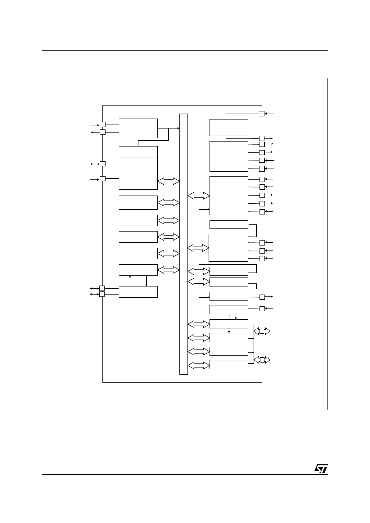
Figure 1. L9805 Block Diagram
8-BIT CORE
ALU
ADDRESS AND DATA BUS
OSCIN
OSCOUT
10-bit ADC
WATCHDOG
OSC
Internal
CLOCK
CONTROL
ROM/O TP/EPR OM
16K
PORT A
PA0 -> PA7
OSC SAFEGUARD
PORT B
PB0 -> PB1
TIMER 1
TIMER 2
PWM 2
PWM 1
PWMI
PWMO
PWMO
AD2
AD3
AD4
RAM 256B
EEPROM 128B
V
CC
V
DD
POWER
SUPPLY
VB2
PREREGULATOR
AGND
GND
NRESET
POWER
BRIDGE
VBR
VBL
PGND
OUTR
OUTL
CAN
CONTROLLER
CAN
TRANSCEIVER
CAN_H
CAN_L
RX TX
TEMP SENSOR
PWMI
VPP/TM
VB1
7/103
L9805
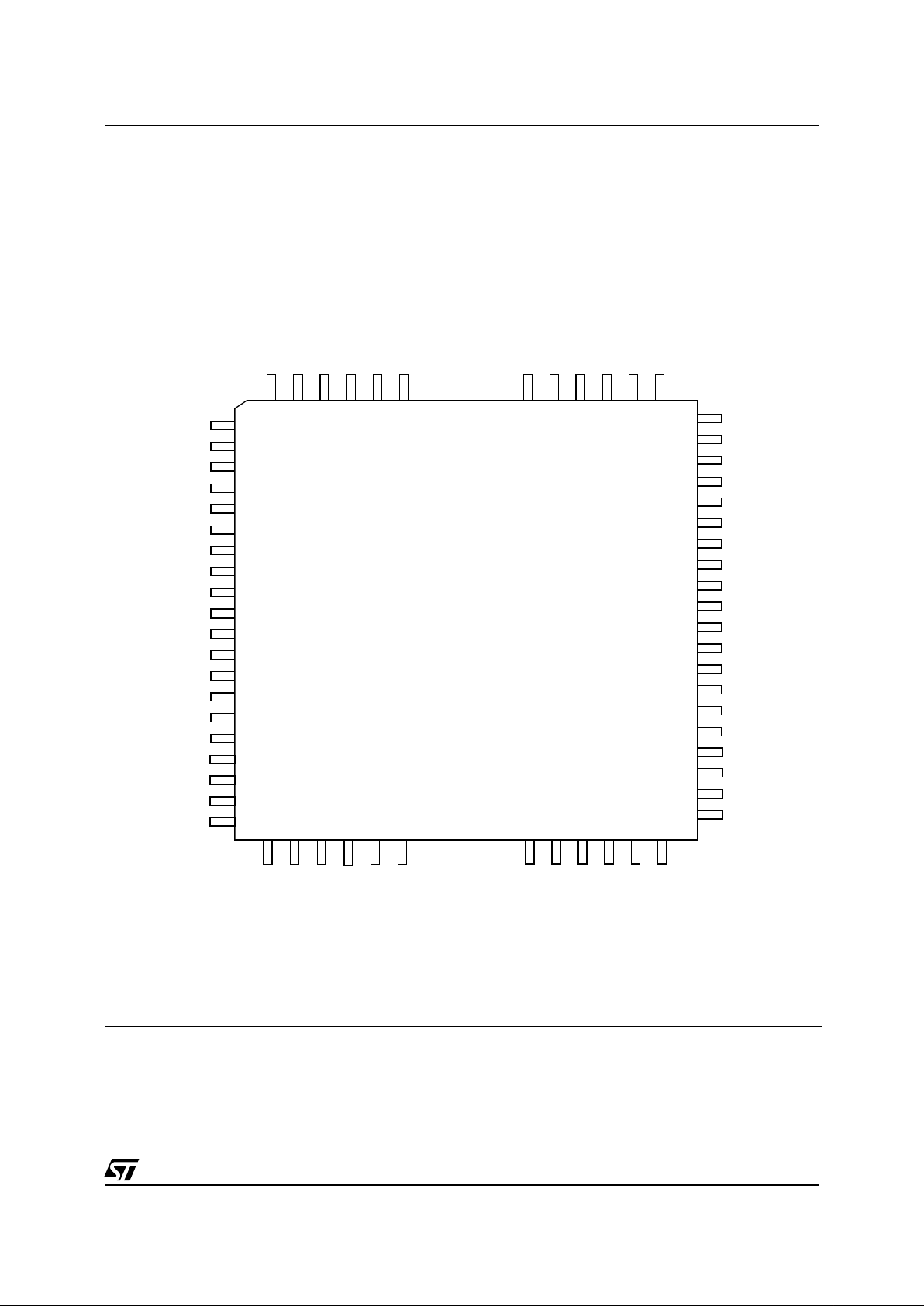
1.3 PIN OUT.
1
2
3
4
5
6
7
8
9
10
11
12
13
14
15
16
48
47
46
45
44
43
42
41
40
39
38
37
36
35
34
33
64 63 62 61 60 59 58 57 56 55 54 53
52
51
50
49
17
18
19
20
21 22 23 24
29 30 31 32
25 26
27 28
NU
NU
NU
AD3
AD2
PA1/OCMP1_1
PA0/OCMP2_1
VPP/TM
VDD
OSCIN
OSCOUT
GND
NU
VBL
VBL
VBL
NU
NU
NU
NU
NU
PB1/EXTCLK_2
NU
NU
PWMO
PWMI
NRESET
CAN_H
CAN_L
GND
VDD
VB2
VB1
VBR
VBR
VBR
NU
NU
NU
NU
NU
NU
OUTL
OUTL
OUTL
PGND
PGND
OUTR
OUTR
OUTRNUNU
VCC
AGND
AD4
PA2/ICAP2_1
PA3/ICAP1_1
PGND
PGND
PA4/EXTCLK_1
PA5/OCMP2_2
PA6/OCMP1_2
PA7/ICAP2_2
PB0/ICAP1_2

8/103
L9805
1.4 PIN DESCRI PTION
AD2-AD4:
Analog input to ADC.
PA0/OCMP2_1-PA1/OCMP1_1:
I/Os or Output
compares on Timer 1.
Alternate function software
selectable (by setting OC2E or OC1 E in CR2 register: bit 6 or 7 at 0031h). When used as an alternate function, this pin is a pus h-pull output as requested by Timer 1. Otherwise, this pin is a triggered floating input or a push-pull output.
PA2/ICAP2_1-PA3/ICAP1_1:
I/
Os or Input cap-
tures on Timer 1.
Before using this I/O as alternate
inputs, they must be configured by software in input mode (DDR=0). In this case, these pins are a
triggered floating input. Otherwise (I/O function),
these pin are triggered floating inputs or push-pull
outputs.
PA4/EXTCLK_1:
PA4 I/O or External Clock on
Timer 1
. Before using this I/O as alternate input, it
must be configured by software in input mode
(DDR=0). In this case, this pin is a triggered floating input. Otherwise (I/O function), this pin is a triggered floating input or a push-pull output.
PA5/OCMP2_2-PA6/OCMP1_2:
I/Os or Output
Compares on Timer 2
. Alternate function software
selectable (by setting OC2E or OC1 E in CR2 register: bit 6 or 7 at 0041h). When used as alt ernate
functions, these pins are push-pull outputs as requested by Timer 2. Otherwise, these pins are triggered floating inputs or push-pull outputs.
PA7/ICAP2_2-PB0/ICAP1_2:
I/Os or Input Cap-
tures on Timer 2
. Before using these I/Os as alternate inputs, they must be configured by softw are
in input mode (DDR=0). In this case, these pins
are triggered floating inputs. Otherwise (I/O function), these pins are triggered floating inputs or
push-pull outputs.
PB1/EXTCLK_2:
PB1 I/O or External Clock on
Timer 2
. Before using this I/O as alternate input, it
must be configured by software in input mode
(DDR=0). In this case, this pin is a triggered floating input. Otherwise (I/O function), this pin is a triggered floating input or a push-pull output.
VPP/TM
: Input. This pin must be held low du ring
normal operating modes.
VDD
: Output. 5V Power supply for digital circuits,
from internal voltage regulator.
OSCIN:
Input Oscillator pin.
OSCOUT
: Output Oscillator pin.
GND:
Ground for digital circuits.
VBR:
Power supply for Right half-bridge.
OUTR:
Output of Left half-bridge.
PGND:
Ground for power transistor.
OUTL:
Output of Right half-bridge.
VBL:
Power supply for Left half-bridge.
VB1
: Power supply for voltage regulators.
VB2
: Pre-regulated voltage for analog circuits.
CAN_L:
Low side CAN bus output.
CAN_H:
High side CAN bus input.
NRESET:
Bidirectional. This active low signal forces the initialization of the MCU. This event is the
top priority non maskable interrupt. It can be us ed
to reset external peripherals.
PWMI:
PWM input.
Directly connected to Input
Capture 2 on Timer 2.
PWMO:
PWM output.
Connected to the output of
PWM2 module.
AGND:
Ground for all analog circuitry (except
power bridge)
.
VCC:
Output. 5V power supply for analog circuits,
from internal voltage regulator.
9/103
L9805
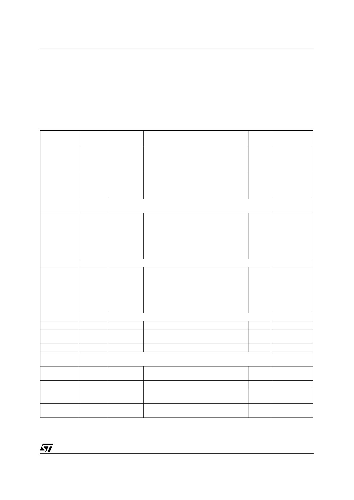
1.5 REGISTER & MEMORY MAP
As shown in the Table 1, the MCU is capable of
addressing 64K bytes of memories and I/O registers. In this MCU, 63742 of these bytes are user
acce ssib le.
The available memory locations consist of 128
bytes of I/O registers, 256 bytes of RAM, 128
bytes of EEPROM and 16Kbytes of user EPROM/
ROM. The RAM space includes 64bytes for the
stack from 0140h to 017Fh.
The highest address by tes contain the user re set
and interrupt vectors.
Table 1. Memory Map
Address Block
Register Label
Register name
Reset
Status
Remarks
0000h
0001h
0002h
0003h
Port A
PADR ..
PADDR ..
PAOR ..
Data Register
Data Direction Register
Option Register
Not Used
00h
00h
00h
R/W
R/W
R/W
Absent
0004h
0005h
0006h
0007h
Port B
PBDR ..
PBDDR ..
PBOR ..
Data Register
Data Direction Register
Option Register
Not Used
00h
00h
00h
R/W
R/W
R/W
Absent
0008h to
000Fh
RESERVED
0010h
0011h
0012h
0013h
0014h
0015h
0016h
PWM1
P1CYRH ..
P1CYRL ..
P1DRH ..
P1DRL ..
P1CR ..
P1CTH ..
P1CTL ..
PWM1 Cycle Register High
PWM1 Cycle Register Low
PWM1 Duty Register High
PWM1 Duty Register Low
PWM1 Control Register
PWM1 Counter Register High
PWM1 Counter Register Low
00h
00h
00h
00h
00h
00h
00h
R/W
R/W
R/W
R/W
R/W
Read Only
Read Only
0017h RESERVED
0018h
0019h
001Ah
001Bh
001Ch
001Dh
001Eh
PWM2
P2CYRH ..
P2CYRL ..
P2DRH ..
P2DRL ..
P2CR ..
P2CTH ..
P2CTL ..
PWM2 Cycle Register High
PWM2 Cycle Register Low
PWM2 Duty Register High
PWM2 Duty Register Low
PWM2 Control Register
PWM2 Counter Register High
PWM2 Counter Register Low
00h
00h
00h
00h
00h
00h
00h
R/W
R/W
R/W
R/W
R/W
Read Only
Read Only
001Fh RESERVED
0020h MISCR .. Miscellaneous Register 00h see Section 3.4
0021h
Power
Bridge
PBCSR .. Bridge Control Status Register 00h R/W
0022h DCSR .. Dedicated Control Status Register 00h R/W
0023h to
0029h
RESERVED
002Ah
002Bh
WDG
WDGCR ..
WDGSR ..
Watchdog Control Register
Watchdog Status Register
7Fh
00h
R/W
R/W
002Ch EEPROM EECR .. EEPROM Control register 00h R/W
002Dh
002Eh
EPROM
ECR1
ECR2
EPROM Control register 1
EPROM Control register 2
ST INTERNAL
USE ONLY
002Fh
0030h
CRC
CRCL
CRCH
CRCL Test Register
CRCH Test Register
ST INTERNAL
USE ONLY
10/103
L9805
0031h
0032h
0033h
0034h-0035h
0036h-0037h
0038h-0039h
003Ah-003Bh
003Ch-003Dh
003Eh-003Fh
TIM1
T1CR2 ..
T1CR1 ..
T1SR ..
T1IC1HR ..
T1IC1LR ..
T1OC1HR ..
T1OC1LR ..
T1CHR ..
T1CLR ..
T1ACHR ..
T1ACLR ..
T1IC2HR ..
T1IC2LR ..
T1OC2HR ..
T1OC2LR ..
Timer 1 Control Register2
Timer 1 Control Register1
Timer 1 Status Register
Timer 1 Input Capture1 High Register
Timer 1 Input Capture1 Low Register
Timer 1 Output Compare1 High Register
Timer 1 Output Compare1 Low Register
Timer 1 Counter High Register
Timer 1 Counter Low Register
Timer 1 Alternate Counter High Register
Timer 1 Alternate Counter Low RegisteR
Timer 1 Input Capture2 High Register
Timer 1 Input Capture2 Low Register
Timer 1 Output Compare2 High Register
Timer 1 Output Compare2 Low Register
00h
00h
xxh
xxh
xxh
xxh
xxh
FFh
FCh
FFh
FCh
xxh
xxh
xxh
xxh
R/W
R/W
Read Only
Read Only
Read Only
R/W
R/W
Read Only
Read Only
Read Only
Read Only
Read Only
Read Only
R/W
R/W
0040h Reserved: Write Forbidden
0041h
0042h
0043h
0044h-0045h
0046h-0047h
0048h-0049h
004Ah-004Bh
004Ch-004Dh
004Eh-004Fh
TIM2
T2CR2 ..
T2CR1 ..
T2SR ..
T2IC1HR ..
T2IC1LR ..
T2OC1HR ..
T2OC1LR ..
T2CHR ..
T2CLR ..
T2ACHR ..
T2ACLR ..
T2IC2HR ..
T2IC2LR ..
T2OC2HR ..
T2OC2LR ..
Timer 2 Control Register2
Timer 2 Control Register1
Timer 2 Status Register
Timer 2 Input Capture1 High Register
Timer 2 Input Capture1 Low Register
Timer 2 Output Compare1 High Register
Timer 2 Output Compare1 Low Register
Timer 2 Counter High Register
Timer 2 Counter Low Register
Timer 2 Alternate Counter High Register
Timer 2 Alternate Counter Low Register
Timer 2 Input Capture2 High Register
Timer 2 Input Capture2 Low Register
Timer 2 Output Compare2 High Register
Timer 2 Output Compare2 Low Register
00h
00h
xxh
xxh
xxh
xxh
xxh
FFh
FCh
00h
00h
xxh
xxh
xxh
xxh
R/W
R/W
Read Only
Read Only
Read Only
R/W
R/W
Read Only
Read Only
Read Only
Read Only
Read Only
Read Only
R/W
R/W
0050h to
0059h
RESERVED
005Ah
005Bh
005Ch
005Dh
005Eh
005Fh
0060h to
006Fh
CAN
CANISR ..
CANICR ..
CANCSR ..
CANBRPR ..
CANBTR ..
CANPSR ..
CAN Interrupt Status Register
CAN Interrupt Control Register
CAN Control/Status Register
CAN Baud Rate Prescaler
CAN Bit Timing Register
CAN Page Selection
CAN First address to
last address of PAGE X
00h
00h
00h
00h
23h
00h
--
R/W
R/W
R/W
R/W
R/W
R/W
see page map-
ping and regis-
ter description
0070h
0071h
0072h
ADC
ADCDRH ..
ADCDRL ..
ADCCSR ..
ADC Data Register High
ADC Data Register Low
ADC Control/Status Register
00h
00h
20h
Read Only
Read Only
R/W
Address Block
Register Label
Register name
Reset
Status
Remarks
11/103
L9805
Address Block Description
0080h to
013Fh
RAM 256
Bytes
including
STACK 64
bytes (0140h
to 017Fh)
User variables and subroutine nesting
0140h to
017Fh
0180h to
0BFFh
RESERVED
0C00h to
0C7Fh
EEPROM 128
bytes
including 4 bytes reserved for temperature sensor trimming (see Section 5.5.6)
0C7CH: T0H
0C7DH: T0L
0C7EH: VT0H
0C7FH: VT0L
0C80h to
BFFFh
RESERVED
C000 to
FFDFh
EPROM 16K
bytes
(16384 bytes)
User application code and data
FFE0h to
FFFFh
Interrupt and Reset Vectors
12/103
L9805
2 CENTRAL PRO CESSING UNIT
2.1 INTRODUCTION
The CPU has a full 8-bit architecture. Six internal
registers allow efficient 8-bit data manipulation.
The CPU is capable of executing 63 basic instructions and features 17 main addressing modes.
2.2 CPU REGISTERS
The 6 CPU registers are shown in the program ming model in F igure 2, on page 12. Following an
interrupt, all registers except Y are pushed onto
the stack in the order shown in Figure 3, on
page 13. They are popped from stack in the reverse order.
The Y register is not affected by these automatic
procedures. The interrupt routine must therefore
handle Y, if needed, through the PUS H and POP
instructions.
Accumulator (A).
The Accumulator is an 8-bit
general purpose register used to hold operands
and the results of the a rithmetic and logic calculations as well as data manipulations.
Index Registers (X and Y).
These 8-bit reg isters
are used to create ef fective address es or as temporary storage areas for data manipulation. The
Cross-Assembler generates a PRECEDE instruction (PRE) to indicate that the following instruction
refers to the Y register.
Program Counter (PC).
The program counter is a
16-bit register containing the address of the next
instruction to be executed by the CPU.
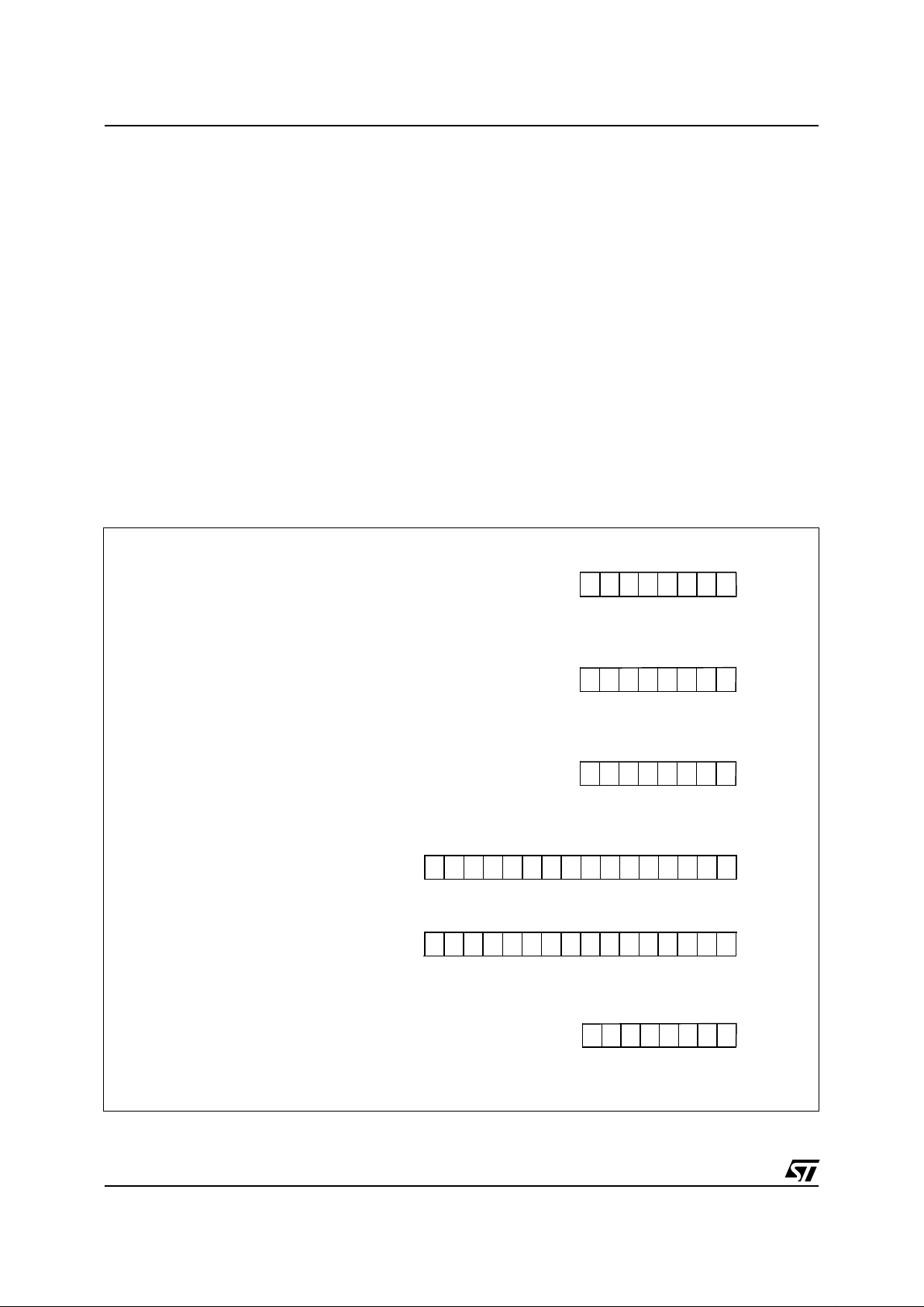
Figure 2. Organi z at io n of In t ernal CPU Regi st ers
ACCUMULATOR:
X INDEX REGISTER:
Y INDEX REGISTER:
STACK POINTER:
CONDITION CODE REGISTER:
PROGRAM COUNTER:
X = Undefined
15
RESET VALUE:
70
XXXXXXXX
RESET VALUE:
70
1X11X1XX
1C11HI NZ
RESET VALUE = RESET VECTOR @ FFFEh-FFFFh
RESET VALUE:
70
XXXXXXXX
RESET VALUE:
70
XXXXXXXX
70
15
70
01000000
RESET VALUE =0 0 0 0 0 0 0 1 0 1 1 1 1 1 1 1
13/103
L9805
CPU REGISTERS
(Cont’d)
Stack Pointer (SP)
The Stack Pointer i s a 16-bit
register. Since the stack is 64 bytes deep, the
most significant bits are forced as indicated in
Figure 2, on page 12 in order to address the stack
as it is mapped in memory.
Following an MCU Reset, or after a Reset Stack
Pointer in stru ction (R SP), the S tac k Po inte r is s et
to point to the next free location in the s tack. It is
then decremented after data has been pushed
onto the stack and incremented before data is
popped from the stack.
Note:
When the lower limit is exceeded, the Stack
Pointer wraps around to the stack upper limit, without indicating the stack overflow. The previously
stored information is then overwritten and therefore lo s t.
The upper and lower limits of the stack area are
shown in the Memory Map.
The stack is used to save the CPU context durin g
subroutine calls or interrupts. The user may also
directly manipulate the stack by means of the
PUSH and POP instructions. In the cas e of an interrupt (refer to Figure 3), the PCL is stored at the
first location pointed to by t he SP. Then the other
registers are stored in the next locations.
– When an interrupt is received, the SP is decre-
mented and the context is pushed on the stack.
– On return from interrupt, the SP is incremented
and the context is popped from the stack.
A subroutine call occupies two locations and an interrupt five locations in the stack area.
Condition Code Register (CC)
The Condition
Code register is a 5-bit register which indicates the
result of the instruction just executed as well as the
state of the processor. These bits can be individually tested by a program and specified action taken
as a result of their state. The following paragraphs
describe each bit of the CC register in turn.
Half carry bit (H)
The H bit is set to 1 when a carry
occurs between bits 3 and 4 of t he ALU during an
ADD or ADC instruction. The H bit is useful in BCD
arithmetic subroutines.
Interrupt mask (I)
When the I bit is set to 1, all interrupts except the TRAP software interrupt are
disabled. Clearing this bi t enables interrupts to be
passed to the processor core. Interrupts requested
while I is set are latched and can be processed
when I is cleared (only one interrupt request per interrupt enable flag can be latched).
Negative (N)
When set to 1, t his bit indic ates that
the result of the last arithmetic, logical or data manipulation is negative (i.e. the most significant bit is
a logic 1).
Zero (Z)
When set to 1, this bit indicate s that the
result of the last arithmetic, logical or data manipulation is ze ro .
Carry/Borrow (C)
When set, C indicates that a
carry or borrow out of the ALU occured du ring the
last arithmetic operation. This bit is also affected
during execution of bit test, branch, shift, rotate
and store instructions.
Figure 3. Sta ck Manipulatio n on Inte rrupt
CONDITION CODE
ACCUMULATOR
X INDEX REGISTER
PCH
PCL
111
0
7
HIGHER ADDRESS
LOWER ADDRESS
CONTEXT RESTORED
CONTEXT SAVED
ON INTERRUPT
ON RETURN
14/103
L9805
3 CLOCKS, RESET, INTERRUPTS & POWER SAVI NG MODES
3.1 CLOCK SYSTEM
3.1.1 General Description
The MCU accepts either a Crystal or Ceramic resonator, or an external clock signal to drive the internal oscillator. The internal clock (f
CPU
) is de-
rived from the external os cillator frequency (f
OSC).
The external Oscillator clock is first divided by 2,
and an additional division factor of 2, 4, 8, o r 16
can be applied, in Slow Mode, to reduce the frequency of the f
CPU
; this clock signal is also routed
to the on-chip peripherals (except the CAN). The
CPU clock signal con si sts of a square wave with a
duty cycle of 50%.
The internal oscillat or is designed to operate with
an AT-cut parallel resonant quartz crystal resonator in the frequency range specified for f
osc
. The
circuit shown in Figure 5 is recommended when
using a crystal, and Tab le 2 lists the recommended capacitance and feedback resistance values.
The crystal and associated components should be
mounted as close as p ossible to the input pins i n
order to minimize output distortion and start-up
stabilisation time.
Use of an external CMOS oscillator is recommended when crystals outside the specified frequency ranges are to be used.
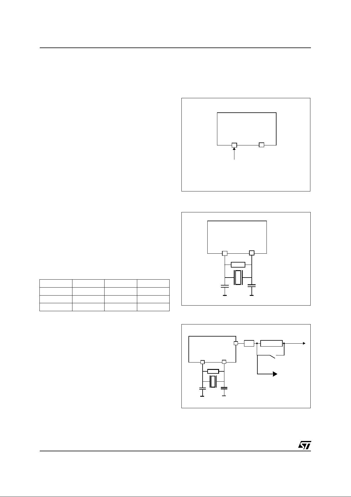
Table 2. Recommended Values for 16 MHz
Crystal Resonator
Note:
R
SMAX
is the equivalent serial resistor of the
crystal (see crystal specification).
C
OSCIN,COSCOUT
:
Maximum total capacitances on
pins OSCIN and OSCOUT (the value includes the
external capacitance tied to the p in plus the parasitic capacitance of the board and of the device).
Rp:
External shunt resistance. Recommended val-
ue for oscillat o r sta bility is 1MΩ.
Figure 4. External Clock Source Connections
Figure 5. Crystal/Ceramic Resonator
Figure 6. Clock Prescaler Block Diagram
R
SMAX
40
Ω
60
Ω
150
Ω
C
OSCIN
56pF 47pF 22pF
C
OSCOUT
56pF 47pF 22pF
R
P
1-10 MΩ 1-10 MΩ 1-10 MΩ
OSC
in
OSC
out
EXTERNAL
CLOCK
NC
OSC
in
OSC
out
C
OSCin
C
OSCout
R
P
OSC
in
OSC
out
C
OSCin
C
OSCout
R
P
%2 %2,4,8,16
CPUCLK
to CPU and
Peripherals
to CAN
15/103
L9805
CLOCK SYSTEM
(Cont’d)
3.1.2 External Clock
An external clock may be applied to the OSCIN input with the OSCOUT pin not connected, as
shown on Figure 4. The t
OXOV
specifications does
not apply when usi ng an external clock input. T he
equivalent specification of the external clock
source should be used instead of t
OXOV
(see ).
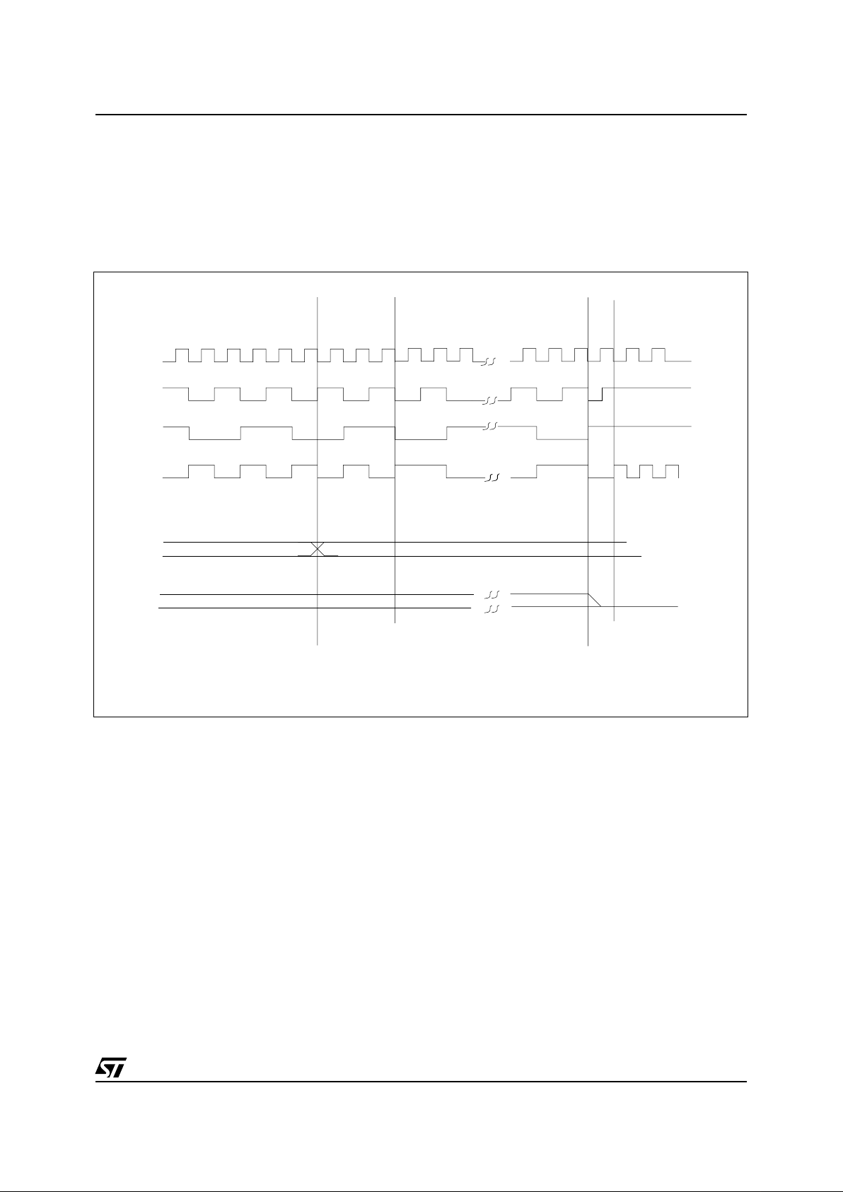
Figure 7. Timing Diagram for Internal CPU Clock Frequency transitions
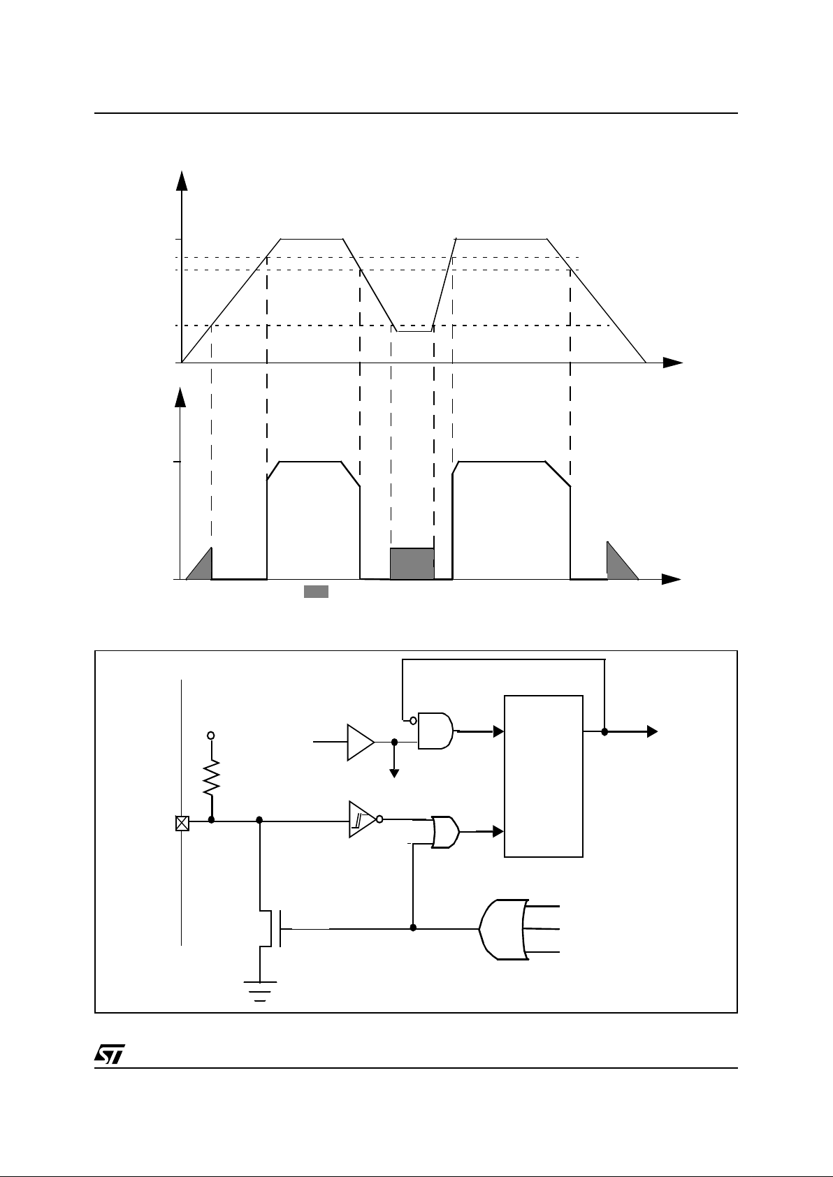
b1 : b2
MISCELLANEOUS REGISTER
00
01
b0
1
1
0
OSC/2
OSC/4
OSC/8
CPU CLK
VR02062B
New frequency
requested
New frequency
active when
osc/4 & osc/8 = 0
Normal mode active
(osc/4 - osc/8 stoppe
d
Normal mode
requested

16/103
L9805
3.2 OSCILLATOR SAFEGUARD
The L9805 contains an oscilla tor safe guard function.
This function provides a real time check of the
crystal oscillator generating a reset condition when
the clock frequency has anomalous value.
If f
OSC<flow
, a reset is generated.
If f
OSC>fhigh,
a reset is generated.
A flag in the Dedicated Control Status Register indicates if the last reset is a safeguard reset.
At the output of reset state the safeguard is disable. To activate the safeguard SFGEN bit must be
set.
Notes:
Following a reset, the safeguard is disabled. Once activated it cannot be disabled, except
by a reset.
3.2.1 Dedicated Control Status Register
DCSR
Address 0022h - Read/Write
Reset Value:xx00 0000 (00h)
b6 =
SGFH:
Safeguard high flag. Set by an Oscillator Safeguard Reset generated for frequency too
high, cleared by software (writing zero) or Power
On / Low Voltage Reset. This flag is useful for distinguishing Safeguard Reset, Power On / Low
Voltage Reset and Watchdog Reset.
b7 =
SGFL:
Safeguard low flag. Set by an Oscillator Safeguard Reset generated for frequency too
low, cleared by software (writing zero) or Power
On / Low Voltage Reset. This flag is useful for distinguishing Safeguard Reset, Power On / Low
Voltage Reset and Watchdog Reset.
b5 =
SFGEN
: Safeguard enable when set. It’s
cleared only by hardware after a reset.
b4 =
CANDS
: CAN Transceiver disable. When this
bit is set the CAN transceiver goes in Power Down
Mode and does not work until this bit is reset.
CANDS is 0 after reset so the standard condition is
with the transceiver enabled. This bit can be used
by application requiring low power consumption
(see Section 5.7 for details).
b3,b2,b1 =
not used
b0 =
PIEN
: PWMI input enable. When set, the
PWMI input line is connected to Input Capture 2 of
Timer 2. Otherwise, ICAP2_2 is the alternate function of PA7. See Figure 31 for the explanation of
this function.
SGFL SGFH SFGEN CANDS
b3b2b
1
PIEN
17/103
L9805
3.3 WATCHDOG SYSTEM (WDG)
3.3.1 Introd uct i on
The Watchdog is used to detect the occurrence of
a software fault, usually generated by external interference or by unforeseen logical conditions,
which causes the application program to give up its
normal sequence. The Watchdog circuit generates
an MCU reset on expiry of a programmed time period, unless the program re freshes the counter’s
contents before it is decremented to zero.
3.3.2 Main Features
– Programm able Time r (64 increments of 12,288
CPU clock)
– Programmable Reset
– reset (if watchdog activated) after an HALT in-
struction or when bit timer MSB reaches zero
– Watchdog Reset indicated by status flag.
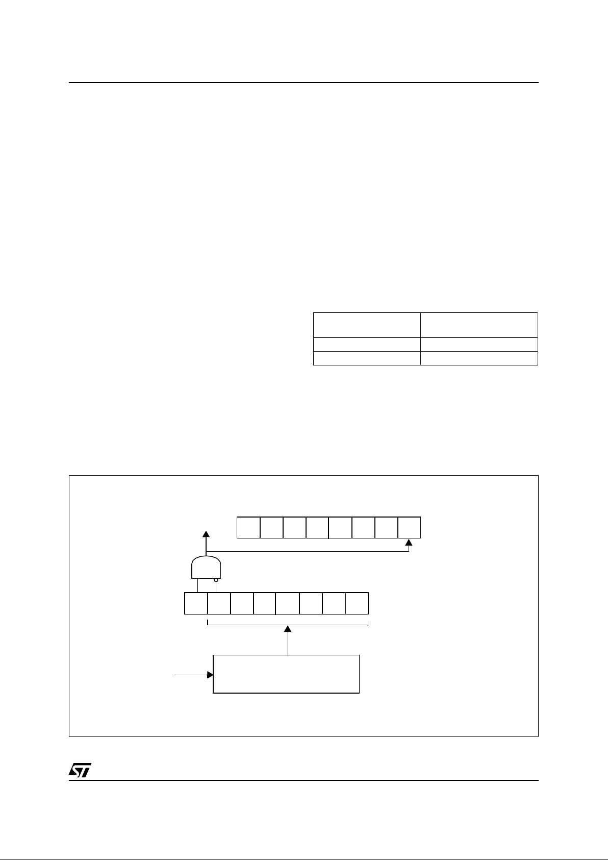
3.3.3 Functional Description
The counter value stored in the CR register (bits
T6:T0), is decremented every 12,288 machine cycles, and the length of the timeout period can b e
programmed by the user in 64 increments.
If the watchdog is activated (the W DGA bit is s et)
and when the 7-bit timer (bits T6:T0) rolls over
from 40h to 3Fh (T6 becom es cleared), it initiates
a reset cycle pulling low the reset pin for typically
500ns.
The application program must write in the CR register at regular intervals during normal operation to
prevent an MCU reset. The value to be stored in
the CR register must be between FFh and C0h
(see Table 1):
– The WDGA bit is set (watchdog enabled)
– The T6 bit is set to prevent generating an imme-
diate reset
– The T5:T0 bit contain the number of increments
which represents the time delay before the
watchdog produces a reset.
Table 3. Wat chdog Timin g (f
OSC
= 16 MHz)
Notes:
Following a reset, the watchdog is disabled. Once activated it cannot be disabled, except
by a reset.
The T6 bit can be used to gen erate a s oftware reset (the WDGA bit is set and the T6 bit is cleared).
If the watchdog is activated, the HALT instruction
will generate a Reset.
Figure 8. Functional Description
WDG Register initial
value
WDG timeout period (ms)
7Fh 98.3
C0h 1.54
RESET
WDGA
7-BIT DOWNCO UNTER
f
CPU
MSB LSB
CLOCK DIVIDE R
WDGF
WATCHDOG STATUS REGISTER (WDGSR)
WATCHDOG CONTROL REGIST ER (WDGCR)
÷12288

18/103
L9805
WATCHDOG SY ST E M
(Cont’d)
The Watchdog delay time is defined by bi ts 5 -0 of
the Watchdog register; bit 6 must always be set in
order to avoid generating an immediate reset.
Conversely, this can be used to generate a software reset (bit 7 = 1, bit 6 = 0).
The Watchdog must be reloaded before bit 6 is decremented to “0” to avoid a Reset. F ollowing a Reset, the Watchdog register will contain 7Fh (bits 0-
7).
If the circuit is not used as a Watchdog (i.e. bit 7 is
never set), bits 6 to 0 ma y be u se d as a simple 7bit timer, for instance as a real t ime clock. Since no
reset will be generated under these conditions, the
Watchdog control register must be monitored by
softw are.
A flag in the watchdog status register indicates if
the last reset is a watchdog reset or not, before
clearing by a write of this register.
3.3.4 Register Description
3.3.4.1 Watchdog Control Register
(WDGCR)
Register Address: 002Ah — Read/Write
Reset Value: 0111 1111 (7Fh)
b7 =
WDGA:
Activation bit.
This bit is set by software and only cleared by
hardware after a reset. When WDGA = 1, the
watchdog can generate a reset.
0: Watchdog disabled
1: Watchdog enabled.
b6-0 =
T6-T0
: 7 bit timer (Msb to Lsb)
These bits contain the decremented value. A reset
is produced when it rolls over from 40h to 3Fh (T6
become cleared).
3.3.4.2 Watchdog Status Register
(WDGSR)
Register Address: 002Bh — Read/W rite
Reset Value
(*)
: 0000 0000 (00h)
b7-1 =
not used
b0 =
WDGF:
Watchdog flag. Set by a Watchdog
Reset, cleared by software (writing zero) or Power
On / Low Voltage Reset. This flag is useful for distinguishing Power On / Low Voltage Reset and
Watchdog Reset.
(*): Except in the case of Watchdog Reset.
70
WDGAT6T5T4T3T2T1T0
70
-------WDGF
19/103
L9805
3.4 MISCELLANEOUS REGISTER
(MISCR)
The Miscellaneous register allows the user to select the Slow operating mode and to set the clock
division prescaler factor. Bits 3, 4 determine the
signal conditions which will trigger an interrupt request on I/O pins having interrupt capability.
Register Address: 0020h — Read/Write
Reset Value:0000 0000 (00h)
b0 -
Slow Mode Select
0- Normal mode - Oscillator frequency / 2
(Reset state)
1- Slow mode (Bits b1 and b2 define the prescaler
factor)
b1, b2 -
CPU clock prescaler for Slow Mode
The selection issued from b3/b4 combination is
applied to PA[0]..PA[7],PB0,PB1 external interrupt. The selection can be made only if I bit in CC
register is reset (interrupt enabled).
b3, b4 can be written only when the Interrupt Mask
(I) of the CC (Condition Code) register is set to 1.
b5,b6,b7 =
not used
b7 b6 b5 b4 b3 b2 b1 b0
b2 b1 Option
00
Oscillator frequency / 4
10
Oscillator frequency / 8
01
Oscillator frequency / 16
11
Oscillator frequency / 32
b4 b3 Option
00
Falling edge and low level (Reset state)
10
Falling edge only
01
Rising edge only
11
Rising and Falling edge

20/103
L9805
3.5 RESET
3.5.1 Introd uct i on
There are four sources of Reset:
– NRESET pin (external source)
– Power-On Reset / Low Voltage Detection (Inter-
nal source)
– WATCHDOG (Internal Source)
– SAFEGUARD (Internal source)
The Reset Service Routine vector is located at ad-
dress FFFEh-FFFFh.
3.5.2 External Reset
The NRESET pin is both an in put and an opendrain output with integrated pull-up resistor. When
one of the internal Reset sources is active, the Reset pin is driven low to reset the whole application.
3.5.3 Reset Operation
The duration of the Reset condition, which is also
reflected on the output pin, is fixed at 4096 internal
CPU Clock cycles. A Reset signal originating from
an external source must have a duration of at least
1.5 internal CPU Clock cycl es in order to b e recognised. At the end of the Power-On Reset cycle, the
MCU may be held in t he Reset condition by an External Reset signal. The NRESET pin may thus be
used to ensure V
DD
has risen to a point where the
MCU can operate correctly before the user program is run. Following a Power-On Reset event, or
after exiting Halt mode, a 409 6 CPU Clock cycle
delay period is initiated in order to allow the oscil-
lator to sta bilise and to ensu re that recovery ha s
taken place from the Reset state.
During the Reset cycle, the device Reset pin acts
as an output that is pulsed low. In i t s high state, an
internal pull-up resistor of about 300KΩ is connected to the Reset pin. This resistor can be pulled
low by external circuitry to reset the device.
3.5.4 Power-on Reset - Low Voltage Detection
The POR/LVD function generates a static reset
when the supply voltage is below a reference value. In this way, the Power-On Reset and Low Voltage Reset function are provided, in order to keep
the system in safe condition when the voltage is
too low.
The Power-Up and Power-Down thresholds are
different, in order to avoid spurious reset when the
MCU starts running and sinks current from the
supply.
The LVD reset circuitry generates a reset when
V
DD
is below:
– V
ResetON
when V
DD
is rising
– V
ResetOFF
when VDD is falling
The POR/LVD function is explained in Figure 9.
Power-On Reset activates the reset pull up tran-
sistor performing a complete chip reset. In the
same way a reset can be triggered by the watchdog, by the safeguard or by external low level at
NRESET pin. An external capacitor connected between NRESET and ground can extend the power
on reset period if required.
21/103
L9805
Figure 9. Power Up/Down behaviour
Figure 10. Reset Block Diagram
= undefined value
5V
t
V
Reset UD
V
Reset OFF
V
Reset ON
5V
t
V
DD
POR/LVD
Internal
RESET
Oscillator
Signal
Counter
NRESET
to ST7
RESET
V
DD
Watchdog Reset
Safeguard Reset
POR/LVD Reset
300K
Reset
CLK
22/103
L9805
3.6 INTERRUPTS
A list of interrupt sources is given in Table 4 below,
together with relevant details for each source. Interrupts are serviced according to t heir order of pri ority, starting with I0, which has the highest priority, and so to I12, which has the lowest priority.
The following list describes the origins for each interrupt lev el:
– I0 connected to Ports PA0-PA7, PB0-PB1
– I1 connected to CAN
– I2 connected to Power Diagnostics
– I3 connected to Output Compare of Timer 1
– I4 connected to Input Capture of TImer 1
– I5 connected to Timer 1 Overflow
– I6 connected to Output Compare of Timer 2
– I7 connected to Input Capture of TImer 2
– I8 connected to Time r 2 Overflow
– I9 connected to ADC End Of Conversion
– I10 connected to PWM 1 Overflow
– I11 connected to PWM 2 Overflow
– I12 connected to EEPROM
Exit from Halt mode may only be triggered by an
External Interrupt on one of the following ports:
PA0-PA7 (I0), PB0-PB1 (I0), or by an Internal Interrupt coming from CAN peripheral (I1).
If more than one input pin of a group connected to
the same interrupt line are selected simultaneously, the OR of this signals generates the interrupt.
Table 4. Interrupt Mapping
Interrupts Register Flag name
Interrupt
source
Vector
Address
Reset N/A N/A - FFFEh-FFFFh
Software N/A N/A - FFFCh-FFFDh
Ext. Interrupt (Ports PA0-PA7,
PB0-PB1)
N/A N/A I0 FFFAh-FFFBh
Receive Interrupt Flag
CAN Status
RXIFi
I1 FFF8h-FFF9hTransmit Interrupt Flag TXIF
Error Interrupt Pending EPND
Power Bridge Short Circuit
Bridge Control
Status
SC
I2 FFF6h-FFF7h
Overtemperature OVT
Output Compare 1
Timer 1 Status
OCF1_1
I3 FFF4h-FFF5h
Output Compare 2 OCF2_1
Input Capture 1
Timer 1 Status
ICF1_1
I4 FFF2h-FFF3h
Input Capture 2 ICF2_1
Timer Overflow Timer 1 Status TOF_1 I5 FFF0h-FFF1h
Output Compare 1
Timer 2 Status
OCF1_2
I6 FFEEh-FFEFh
Output Compare 2 OCF2_2
Input Capture 1
Timer 2 Status
ICF1_2
I7 FFECh-FFEDh
Input Capture 2 ICF2_2
Timer Overflow Timer 2 Status TOF_2 I8 FFEAh-FFEBh
ADC End Of Conversion ADC Control EOC I9 FFE8h-FFE9h
PWM 1 Overflow N/A N/A I10 FFE6h-FFE7h
PWM 2 Overflow N/A N/A I11 FFE4h-FFE5h
EEPROM Programming EEPROM Control E2ITE I12 FFE2h-FFE3h
23/103
L9805
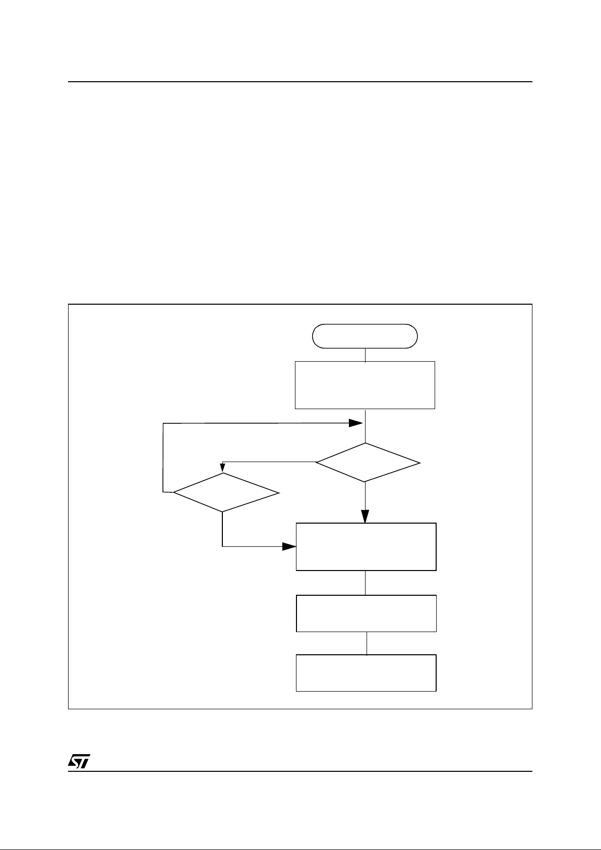
INTERRUPTS
(Cont’d)
Figure 11. Inte rru pt P rocessing Flow c hart
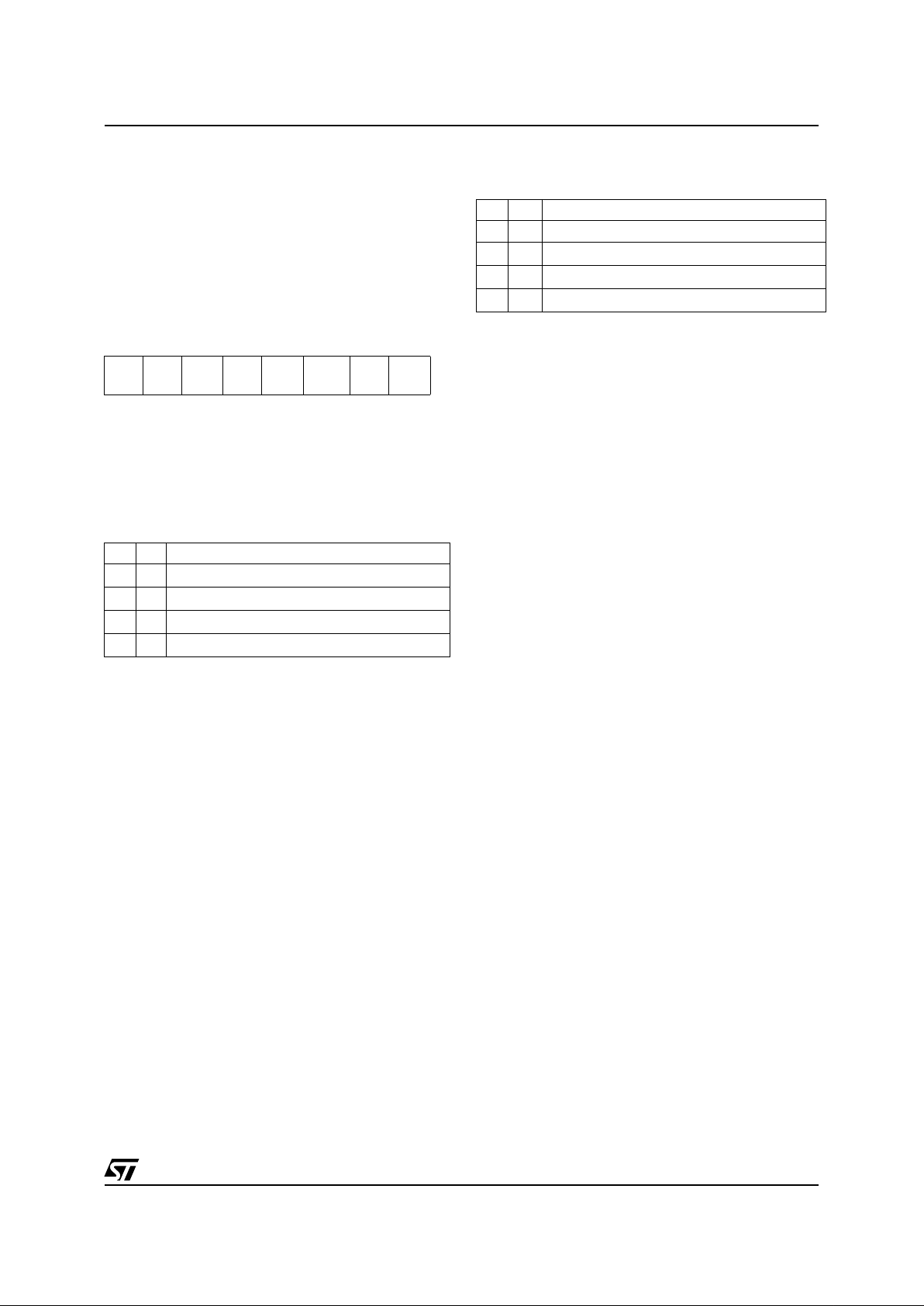
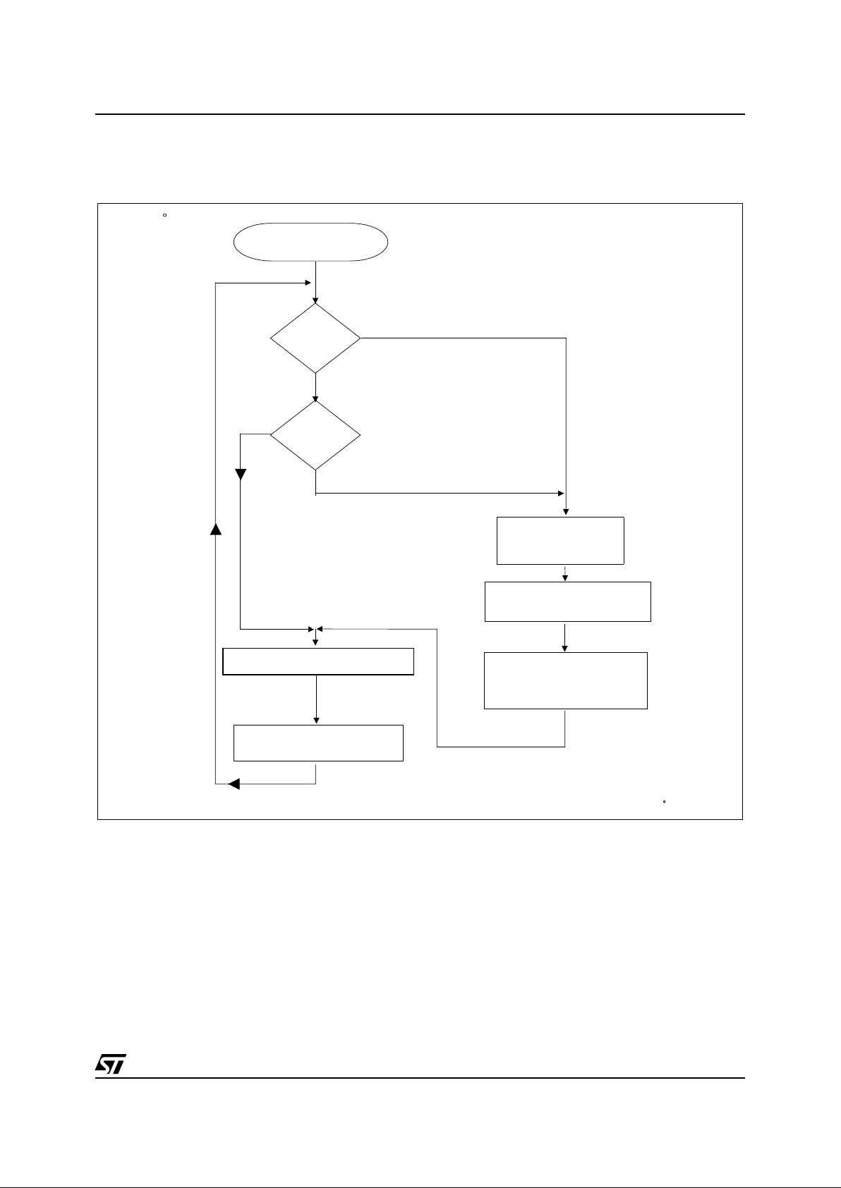
Note
1. See Table 4
INTERRUPT
TRAP
FETCH NEXT
INSTRUCTION
OF APPROPRIATE INTERRUPT
SERVICE ROUTINE
EXECUTE INSTRUCTION
PUSH
PC,X,A,CC
SET I BIT TO 1
VR01172B
N
Y
LOAD PC
WITH APPROPRIATE
INTERRUPT VECTOR
(
1)
I BIT = 1
N
Y
ONTO STACK
24/103
L9805
3.7 POWER SAVI NG MO DE S
3.7.1 Introd uct i on
There are three Power Saving modes. The Slow
Mode may be selected by setting the relevant bit s
in the Miscellaneous register as detailed in Section
3.4. Wait and Halt m odes may be entered usin g
the WFI and HALT instructions.
3.7.2 Slow Mode
In Slow mode, the oscillator frequency can be d ivided by 4, 8, 16 or 32 rathe r than by 2. The CP U
and peripherals (except CAN, see Note) are
clocked at this lower frequency. Slow mode is
used to reduce power consumption.
Note:
Before entering Slow mode and to guarantee low power operations, the CAN Controller
must be placed by software in STANDBY mode.
3.7.3 Wait Mode
Wait mode places the MCU in a low power consumption mode by stopping the CPU. All peripherals remain active. During Wait mode , the I bit (CC
Register) is cleared, so as to enabl e all interrupt s.
All other registers and memory remain unchanged. The MCU will remain in Wait m ode until
an Interrupt or Reset occurs, whereupon the Program Counter branches to t he starting address of
the Interrupt or Reset Service Routine.
The MCU will remain in Wait mode until a Reset or
an Interrupt (coming from CAN, Timers 1 & 2,
EEPROM, ADC, PWM 1 & 2, I/O ports peripherals
and Power Bridge) occurs, causing its wake-up.
Refer to Figure 12 below.
Figure 12. Wait Mode Flow Chart
WAIT INSTRUCTION
RESET
FETCH RESET VECTOR
OR SERVICE INTERRUPT
INTERRUPT
Y
N
N
Y
CPU CLOCK
OSCILLATOR
PERIPH. CLOCK
I-BIT
ON
ON
SET
ON
CPU CLOCK
OSCILLATOR
PERIPH. CLOCK
I-BIT
ON
ON
CLEARED
OFF
25/103
L9805
POWER SAVING MODES
(Cont’d)
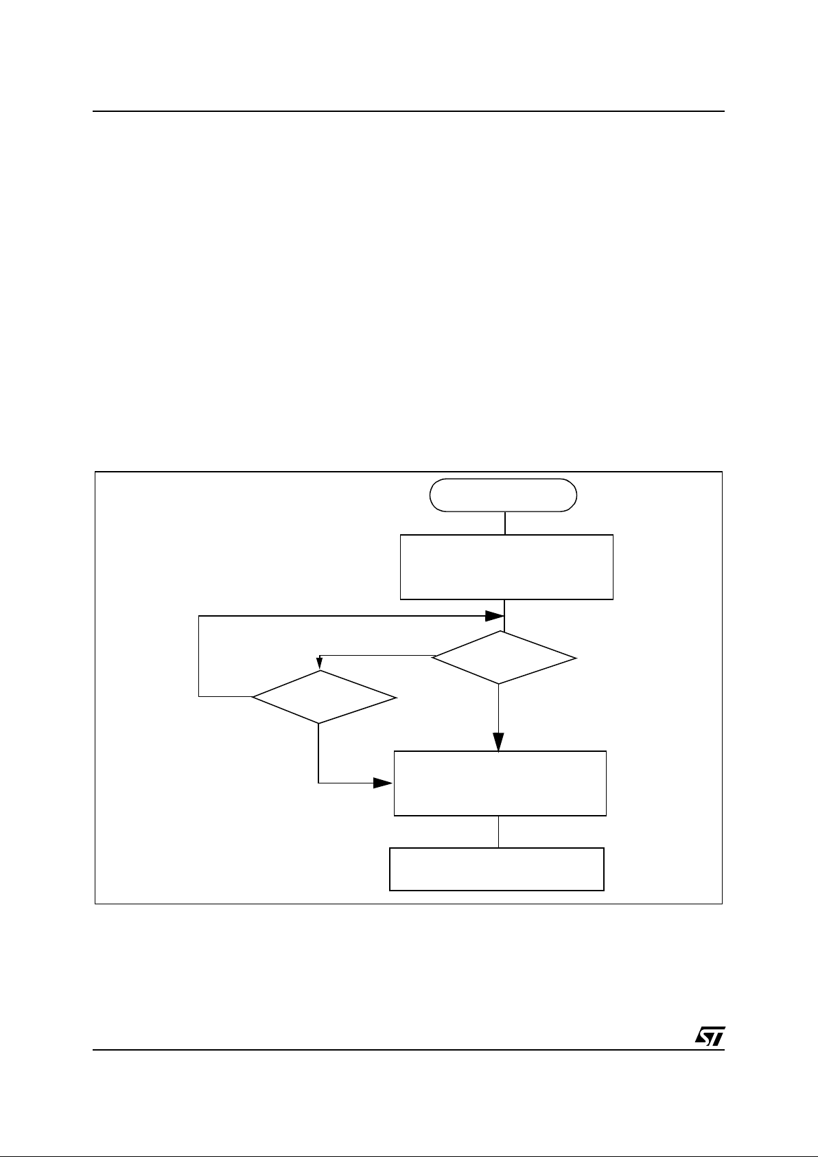
3.7.4 Halt Mode
The Halt mode is the MCU lowest power consumption mode. The Halt mode is entered by executing the HALT instruction. The internal oscillator
is then turned off, causing all internal processing to
be stopped, including the operation of the on-chip
peripherals.
When entering Halt mode, the I bit in the CC Register is cleared so as to enable External Interrupts.
If an interrupt occurs, the CPU becomes active.
The MCU can exit the Halt mode upon reception of
either an external interrupt (I0), a internal interrupt
coming from the CAN peripheral (I1) or a reset.
The oscillator is then turned on and a stabilisation
time is provided before releasing CPU operat ion.
The stabilisation time is 4096 CPU clock cycles.
After the start up delay, the CPU continues operation by servicing the interrupt which wakes it up or
by fetching the reset vector if a reset wakes it up.
Note
The Halt mode cannot be used when the
watchdog or the Safeguard are enabled, if the
HALT instruction is executed while the watchdog
or safeguard system are enabled, a reset is automatically generated thus resetting the entire MCU.
Note
Halt Mode affects o nly the digital section of
the device. All the analog circuit remain in their
status, including ADC, voltage regulators, bus
transceivers and power bridge.
Figure 13. Hal t Mode Flow Cha rt
N
N
EXTERNAL
INTERRUPT
RESET
HALT INSTRUCTION
4096 CPU CLOCK
FETCH RESET VECTOR
OR SERVICE INTERRUPT
CYCLES DELAY
CPU CLOCK
OSCILLATOR
PERIPH. CLOCK
I-BIT
ON
ON
SET
ON
CPU CLOCK
OSCILLATOR
PERIPH. CLOCK
I-BIT
OFF
OFF
CLEARED
OFF
Y
Y
26/103
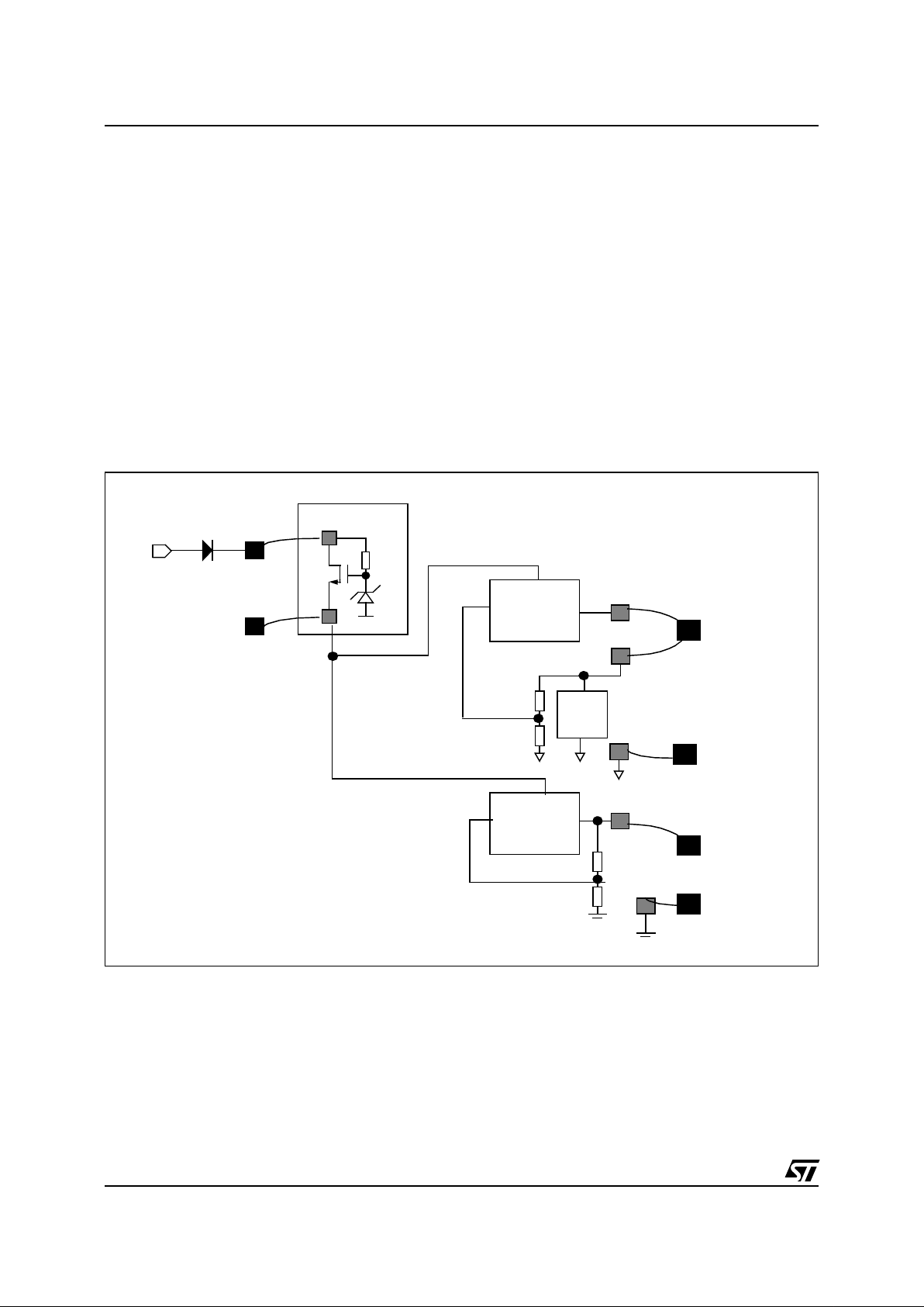
L9805
4 VOLTAGE REGULATO R
4.1 In troduc t ion
The on chip voltage regulator prov ides two regulated voltage, nominally 5V both. VCC supplies
ADC and the analog pe riphery and VDD supplies
the microcontroller and logic pa rts. These voltag e
are available at pins VDD and VCC to supply external components and c onnects a capacitors to
optimize EMI performance. A pre-regulator circuit
allows to connect external tantalum capacitors to a
lower (10V) voltage (VB2 pin).
4.1.1 Functional Description
The main supp ly v oltage is taken from V B 1 pin. A
voltage pre-regulator provides the regulated voltage on pin VB2. VB2 is the supply for the digital
and analog regulators. The bl ock diagram shows
the connections between the regulators and the
external pins.
In order to prevent negative spikes on the battery
line to propagate on the internal supply generating
spurious reset, a series diode suppl y VB1 pin is
recommended.
Figure 14. Vol ta ge regulation bl ock diagram
4.2 Digital Section Power Supply
The digital supply voltage VDD is available at pin
number 42 and 9. The digital ground GND is available at pin number 43 and 12.
Pin 42 and 43 are the actual voltage regulator output and external loads must be supply by these
pin. The 100nF compensation capacitor should be
connected as close as possible to pin 42 and 43.
Pin number 9 and 12 provide an external access to
the internal oscillator supply. Reson ator’s capacitors should be grounded on pin 12.
ADC
PRE-REGULATOR
VB1
VB2
force
ANALOG
VOLTAGE
REGULATOR
sense
VCC
AGND
DIGITAL
VOLTAGE
REGULATOR
VDD(42)
GND(43)
Battery

27/103
L9805
The application board can improve noise reduction
in the chip connecting directly pin 42 to pin 9 and
pin 43 to pin 12 u sing trac es as short as possible.
An additional capacitor mounted close to pin 9 and
12 can lead additional improvement.
4.2.1 VDD Short Circuit Protection
The output current o f the digital voltage regulator
is controlled by a circuit that limits it to a maximum
value (I
MAXVDD
). When the output current exceeds
this value the VDD voltage starts falling down. External loads must be chosen taking in account this
maximum current capability of the regulator.
4.3 Analog Section Power Supply
The analog supply voltage is available on VCC
pin. The external 100nF com pensation capacitor
should be placed as close as possibl e to this pin
and AGND pin.
VCC is the reference voltage f or the AD conversion and must be used to s upply ratiometric sensors feeding AD inputs. Any voltage drop between
VCC pin and the sensor supply pin on the application board, will cause the ADC to be inaccurate
when reading the sensor’s output.
4.3.1 VCC Short Circuit Protection
The output current of th e anal og v oltage regulat or
is controlled by a circuit that limits it to a maximum
value (I
MAXVCC
). When the output current exceeds
this value the VCC voltage starts falling down. External loads must be chosen taking in account this
maximum current capability of the regulator.
WARNING: The pin VB2 i s not short circuit protected so a short circuit on this pin will destroy the
device.

28/103
L9805
5 ON-CHIP PERIPHERALS
5.1 I/O PORTS
5.1.1 Introd uct i on
The internal I/O ports allow the transfer of data
through digital inputs and outputs, the interrupt
generation coming from an I/O and for specific
pins, the input/output of alternate signals for the
on-chip peripherals (TIMERS...).
Each pin can be programmed independently as
digital input (with or without interrupt generation)
or digital output.
5.1.2 Functional Description
Each I/O pin m ay be programmed indepen dently
as a digital input or a digital output, using the corresponding register bits.
Each port pin of the I/O Ports can be individual ly
configured under software control as either i nput
or output.
Each bit of a Data Direction Register (DDR) corresponds to an I/O pi n of the associated po rt. This
corresponding bit must be set to configure its associated pin as output and must be cleared to configure its associated pin as input. The Data Direction Registers can be read and written.
5.1.2.1 Input Mode
When DDR=0, the corresponding I/O is configured
in Input mode.
In this case, the output buffer is switched off, the
state of the I/O is readable through the Data Register address, but the I/O state comes directly from
the Schmitt-Trigger output and not from the Dat a
Register output.
5.1.2.2 Interrupt function
When an I/O is configured in Input with Interrupt
generation mode (DDR=0 and OR=1), a low level
or any transition on this I/O (according to the Miscellaneous register configuration - see Section
3.4, “b3, b4 External Interrupt Option”) will gener-
ate an Interrupt request to the CPU.
Each pin can independently generate an Interrupt
request. When at least one of the interrupt inp uts
is tied low, the port’s common interrupt will activate
a CPU interrupt input according to the e xternal interrupt option in the Miscellaneous Register.
5.1.2.3 Output Mode
When DDR=1, the corresponding I/O is configured
in Output mode. In this mode, the interrupt function
is disabled.
The output buffers c an be individually configured
as Open Drain or Push-Pull b y means of the Option Register.
The output buffer is activated according to the
Data Register’s content.
A read operation is directly performed from the
Data Register output.
5.1.2.4 Alternate function
A signal coming from a on-chip peripheral can be
output on the I/O.
In this case, the I/O is automaticall y configured in
output mode (without pull-up).
This must be controlled directly by the peripheral
with a signal coming from the peripheral which enables the alternate signal to be output.
The I/O’s state is readable as in normal mode by
addressing the corresponding I/O Data Register.
A signal coming from an I/O can be inpu t in a onchip peripheral.
Before using an I/O as Alternate Input, it must be
configured in Input without interrupt mode (DDR=0
and OR=0). So, bot h Alternat e In put co nfigurat ion
(with or without pull-up) and I/O input configuration
(with or without pull-up) are the same.
The signal to be input in the peripheral is taken after the Schmitt-trigger. The I/O’s state is reada ble
as in normal mode by address ing the corres ponding I/O Data Register.
29/103
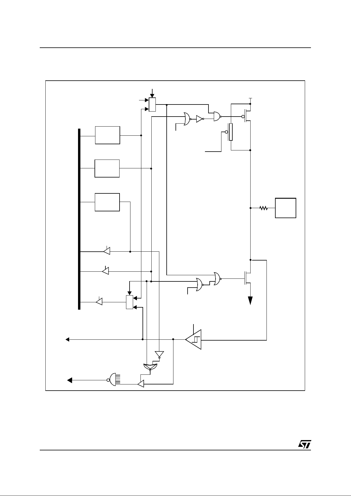
L9805
I/O PO R T S
(Cont’d)
5.1.2.5 I/O Port Implementation
The I/O port register configurations are resumed
as following.
Port PA(7:0), Port PB(2:0)
RESET status: DR=0, DDR=0 and OR=0 (Input
mode, no interrupt).
These ports offer interrupt capabilities.
5.1.2.6 Dedicated Configurations
Table 5. Port A Configuration
Table 6. Port B Configuration
DDR OR MODE
00
input
no interrupt (pull-up enabled)
01
input
interrupt (pull-up enabled)
1 0 Open-Drain output
1 1 Push-Pull output
PORT A
I / O Function
Input Output Alternate Interrupt
PA0 triggered with pull-up push-pull/open drain
OCMP2_1: Output Compare
#2 Timer 1
wake-up interrupt
(I0)
PA1 triggered with pull-up push-pull/open drain
OCMP1_1: Output Compare
#1 Timer 1
wake-up interrupt
(I0)
PA2 triggered with pull-up push-pull/open drain
ICAP2_1: Input Capture #2
Timer 1
wake-up interrupt
(I0)
PA3 triggered with pull-up push-pull/open drain
ICAP1_1: Input Capture #1
Timer 1
wake-up interrupt
(I0)
PA4 triggered with pull-up push-pull/open drain
EXTCLK_1: External Clock
Timer 1
wake-up interrupt
(I0)
PA5 triggered with pull-up push-pull/open drain
OCMP2_2: Output Compare
#2 Timer 2
wake-up interrupt
(I0)
PA6 triggered with pull-up push-pull/open drain
OCMP1_2: Output Compare
#1 Timer 2
wake-up interrupt
(I0)
PA7 triggered with pull-up push-pull/open drain
ICAP2_2: Input Capture #2
Timer 2
wake-up interrupt
(I0)
PORT B
I / O Function
Input Output Alternate Interrupt
PB0 triggered with pull-up push-pull/open drain
ICAP1_2: Input Capture #1
Timer 2
wake-up interrupt
(I0)
PB1 triggered with pull-up push-pull/open drain
EXTCLK_2: External Clock
Timer 2
wake-up interrupt
(I0)
PB2
1)
Note 1. The PB2 bit is not connected to the external. It must be configured as an Input without interrupt, to be used only as an alter nate
function.
Not connected to pad Not connected to pad PWMI: PWM input
30/103
L9805
I/O PO R T S
(Cont’d)
Figure 15
.
Ports PA0-PA7, PB0-PB1
I
DR
DDR
latch
latch
Data Bus
DR SEL
DDR SEL
VDD
PAD
M
U
X
Alternate
Alternate
digital enable
Alternate enable
Alternate
M
U
X
Alternate inpu t
output
P-BUFFER
N-BUFFER
1
0
1
0
OR
latch
OR SEL
from
other
bits
Interrupt
Pull-up
condition
enable
enable
GND
 Loading...