

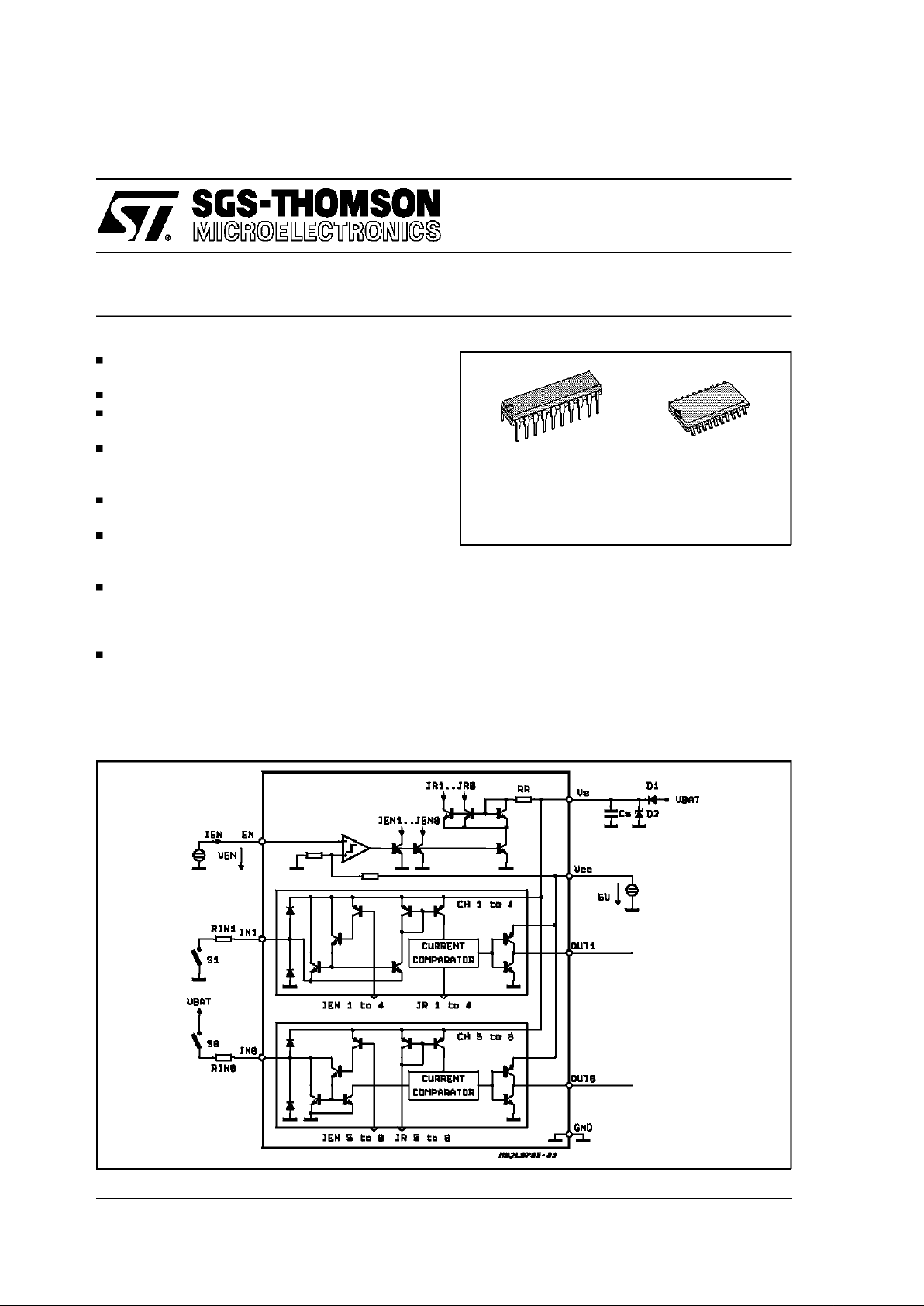
L9705
DOUBLE QUAD CONTACT INTERFACE CIRCUIT
ADVANCE DATA
OPERATINGDC SUPPLY VOLTAGE RANGE
5V TO 25V
SUPPLYOVERVOLTAGEPULSEUP TO 40V
VERY LOW STAND-BY QUIESCENT CUR-
RENT, MAX50µA
INTERNALCLAMPINGDIODESAT CONTACT
INPUTS TO Vs AND gnd WITH PULSE CURRENT CAPABILITYUPTO +50mA,-75mA
CHIP ENABLE FUNCTION AND TRISTATE
OUTPUTS FOR PARALLELBUS CONNECTION
NOMINAL CONTACT CURRENTS OF 10mA
DEFINED WITH EXTERNAL CONTACT SERIES RESISTORSR
IN1-8
CONTACT STATUS MONITORING BY
MEANS OF COMPARING THE RESISTANCE
AT CONTACT SENSE INPUTS WITH THE INTERNAL REFERENCERESISTORVALUE
RESISTANCE COMPARING WITH HYSTERESIS FOR HIGH NOISE IMMUNITY AND IMMUNITY TO GROUND AND BATTERY POTENTIALDIFFERENCES
DESCRIPTION
The L9705 is a bipolar monolithic integrated circuit for monitoring the status of up to four contacts connected to GND and up to four contacts
connectedto the battery. The contact sense input
supply the contact current and perform the contactresistance comparison function.
At the output the contact status is translated into
a logical LOW level (contact closed) or logical
HIGhlevel (contact open).
This isadvanced information on a new product now in development or undergoing evaluation. Details are subject to change without notice.
January1992
BLOCK DIAGRAM
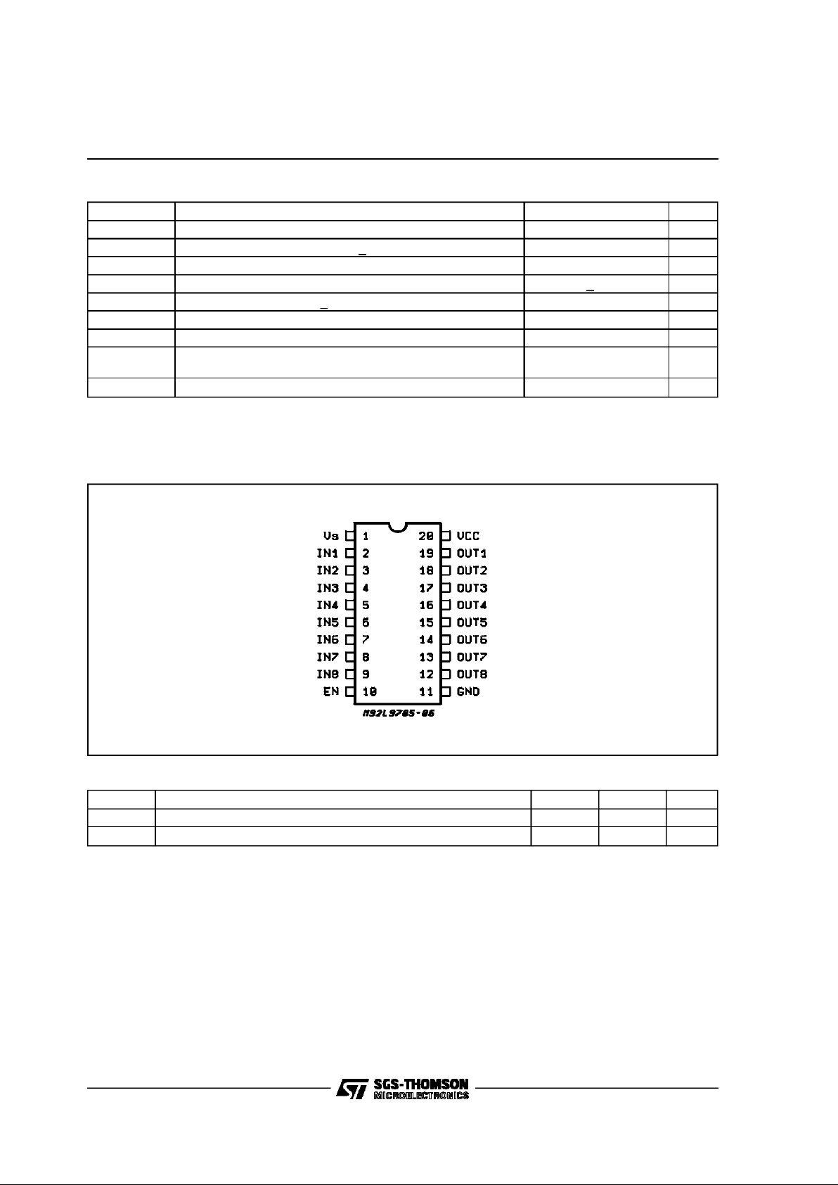
ORDERING NUMBERS : L9705
DIP 20 SO20L
1/8
ABSOLUTE MAXIMUM RATINGS
Symbol Parameter Value Unit
V
SDC
DC Supply Voltage +26 V
V
SP
Peak Transient Supply Voltage (t < 400ms) +40 V
V
CC
Logic Supply Voltage 7 V
I
INDC
Input DC Current +40 mA
I
INP
Input Pulse(tp= 0 to 2ms; f< 0.2Hz; n = 25000) -75 to 50 mA
I
OUT
Output Current (VO = 0 to 5.5V) internally limited
V
EN
Enable Input Voltage VCC+0.3V;-0.3V V
P
tot
TotalPower Dissipation (T
amb
=80°C) DIP 20
SO 20
875
420
mW
mW
T
j
Junction Temperature Range max150 °C
PIN CONNECTION (top view)
THERMAL DATA
Symbol Description DIP20 SO20L Unit
R
th j-amb
Thermal Resistance Junction-ambient 80 °C/W
R
th j-amb
Thermal Resistance Junction-ambient 165 °C/W
L9705
2/8
ELECTRICAL CHARACTERISTICS (VS= 5 to25V, VCC= 4.75 to 5.25V,V
bat
-0.5V <VS,<V
bat
-1V ,
Tj= –40to 150°C unless otherwisespecified.)
Symbol Parameter Test Condition Min. Typ. Max. Unit
V
ENL
Enable Input Voltage LOW
(device activated)
-0.3 0.8 V
V
ENH
Enable Input Voltage HIGH 2.4 V
CC
V
V
ENh
Enable Input Threshold
Hysteresis
200 420 800 mV
I
EN
Enable Input Current 2.4V < VEN<V
CC
0V < VEN< 0.8V -5 -1
5 µA
µA
V
OUTH
Output Voltage HIGH 0 < I
OUT
< 100µA4V
CC
-0.1 V
CC
V
I
OUT
Output Current OUT status= HIGH; V
OUT
= 0 0.5 2 mA
V
OUTL
Output Voltage LOW I
OUT
= -1mA 0.05 0.2 0.4 V
I
OUT
Output Current OUT status= LOW; V
OUT
=5.5V -5 -20 mA
I
OUT TS
Output Tristate Current 0 < VOUT < V
CC
0.5 µA
V
IN 1,4
Input Voltage(device active) EN = LOW;RIN=1KΩ VS-2 VS-1.5 VS-0.4 V
V
IN 5,8
Input Voltage(device active) EN = LOW;RIN=1KΩ 0.4 1.5 2 V
V
IN
Input VoltageDuring Clamp
(device disabled)
EN = HIGH; IIN=30mA
I
IN
= -30mA
V
S
+0.3-2VS+1-1VS+2
-0.3
V
V
R
IL 1,4
Input Resistor LOW Threshold
(note 1)
5V < VS<16V; ∆V
GND
≤ 0.1V
S
∆V
BAT
≤ 0.1V
BAT
1.8 4 KΩ
R
IL 5,8
Input Resistor LOW Threshold
(note 1)
5V < VS<16V; ∆V
GND
≤ 0.1V
S
∆V
BAT
≤ 0.1V
BAT
1.8 4.8 KΩ
R
IH 1,4
Input Resistor HIGH Threshold
(note 1)
5V < VS< 16V; ∆V
GND
≤ 0.1V
S
∆V
BAT
≤ 0.1V
BAT
5.3 20 KΩ
R
IH 5,8
Input Resistor HIGH Threshold
(note 1)
5V < VS<16V; ∆V
GND
≤ 0.1V
S
∆V
BAT
≤ 0.1V
BAT
6.5 29 KΩ
R
IL
Input Resistor Threshold Ratio
(note 1)
5V < VS<16V; ∆V
GND
≤ 0.1V
S
∆V
BAT
≤ 0.1V
BAT
0.65 0.75 0.85
R
IH
Input Resistor Threshold Ratio
(note 1)
5V < VS<16V; ∆V
GND
≤ 0.1V
S
∆V
BAT
≤ 0.1V
BAT
0.65 0.75 0.85
I
QC
Quiescent Current EN = HIGH (t
ENH
>20µs)
V
S
= 5 to 16V; Tj= -40 to 85°C
20 40 µA
I
QS
Quiescent Current all contact open 10 µA
I
QS
Quiescent Current all contact closed 35 µA
ΣI
IN
(2) Quiescent Current ∆V
BAT
≤ 0.1V
BAT
25 µA
I
QC
Quiescent Current EN = LOW 5 mA
I
QS
Quiescent Current EN = LOW 8 mA
t
do
Delay Time/Output (EN LOW to
Output Data Ready) (note 3)
C
OUT
≤ 50pF 15+
3R
IN*CIN
µs
t
dTS
Delay Time/Tristate (EN HIGH
to Output Tristate)(note 3)
C
OUT
≤ 50pF 10 µs
t
dIO
Delay Time Input-Output (note 3) EN = LOW;C
OUT
= 50pF 6 ms
NOTES:
1) The input resistor threshold value is a resistor value from the IN-pin to ground at which the correspondingoutput changes its status (fig.4)
2) ΣI
IN
is the sum of the IN5 to IN8 input currents.
3) The delay times are defined from the crossing point of 50% initiating signal amplitude to the crossing point of 50% output signal amplitude
L9705
3/8

FUNCTIONAL DESCRIPTION
The L9705 circuit monitors the status of the contacts which are connected through the series external resistors R
IN
to the contact sense input
pins. The contacts equivalent circuit is supposed
to be as shown in fig.2 for GND connected contacts (IN 1 to 4) and as shown in fig. 3 for V
BAT
connectedcontacts (IN 5 to 8).
Figure1: Typical applicationdiagram for the L9705 circuit. The currentflowing in the arrow direction is
assumedpositive. The external capacitors C
IN
and C
OUT
representthe totalwiring
capacitanceat the correspondingpins.
Figure2: The contact senseinput connectionwith the contactequivalentcircuit for GND connected
contacts.
Figure3: The contact senseinput connectionwith the contactequivalentcircuit for V
BAT
connected
contacts.
L9705
4/8

The L9705 circuit compares the input current with
the current through the internal reference resistor.
The device is designed to work with an external
input series resistor of R
IN1-8
=1KΩ. With this in-
put resistor the contact current, when the contact
is closedand the deviceactivated (EN =LOW)is:
I
IN
=
V
S
− 2V
1KΩ
,for GND contacts, (1)
I
IN
=
V
BAT
+∆V
BAT
−2V
1KΩ
, for V
BAT
contacts, (2)
For this calculation the limit value of the V
S
to V
IN
and VINsaturation voltage of 2V was considered
so that the lowestlimit value of I
IN
is calculated in
(1)and (2)
Figure4: The output voltage as a functionof theinput resistance at the correspondingsense input.
The function of the circuit can be demonstrated
with the transfer characteristics,showing the output status as a function of the input resistor R
I
,
shown in figure 4. The input resistor is a sum of
the R
IN
and the contact resistance R
CON
or
R
COFF
, for the closed contact:
R
I=RIN+RCON
, (3)
and for the opencontact:
R
I=RIN+RCOFF
,(4)
The output goes HIGH when the input resistance
increases above 5.3KΩ (GND contacts) or 6.5KΩ
(V
BAT
contacts) and goes LOW, when the input
resistance decreases below 4KΩ (GND contacts)
or 4.8KΩ (V
BAT
contacts);these values are typical
values for the switching thresholds.The limit values of R
I
= 1.8KΩ (GND contacts) and RI=
1.8KΩ (V
BAT
contacts) for LOW and RI= 20KΩ
(GND contacts) and 29KΩ (V
BAT
contacts) for
HIGHimplies that a contactwithR
CON
=100Ω(at
I
IN
= 10mA) will be recognized as ON = LOW and
a contact with R
COFF
= 19KΩ (GND contacts) or
28KΩ (V
BAT
contact) will be recognizedas OFF =
HIGH.
These limits are valid within the supply voltage
range 6V < V
S
< 16V, the ground potential differ-
ence of ∆V
GND
=0.1VS, the battery voltage poten-
tial difference of ∆V
BAT
< 0.1V
BAT
and the variation of the reverse battery protection diode D1
voltagefrom 0.5V to 1V.
The internal clamping diodes at the contactmonitoring inputs together with the external contacts
series resistors R
IN
allows to withstand the transients at the contact connection.The contact seriesresistor R
IN
limits the input current at the tran-
sient.
The dynamic behaviour of the circuit is defined
with the times t
do
and t
dTS
. When the contact is
open, the input capacitor C
IN
must be charged
through the resistor R
IN
. In this case the total de-
lay time t
do
may be influenced also with the time
constantR
INCIN
.
The delay time t
dTS
, when disablingthe device, is
defined only with the internal circuitry. In both
cases, output external capacitance less than
50pF is assumed, the internal output capacitance
of the tristatebuffers are less than 5pF.
L9705
5/8

DIP20 PACKAGEMECHANICAL DATA
DIM.
mm inch
MIN. TYP. MAX. MIN. TYP. MAX.
a1 0.51 0.020
B 0.85 1.40 0.033 0.055
b 0.50 0.020
b1 0.38 0.50 0.015 0.020
D 24.80 0.976
E 8.80 0.346
e 2.54 0.100
e3 22.86 0.900
F 7.10 0.280
I 5.10 0.201
L 3.30 0.130
Z 1.27 0.050
L9705
6/8

SO20PACKAGE MECHANICAL DATA
DIM.
mm inch
MIN. TYP. MAX. MIN. TYP. MAX.
A 2.65 0.104
a1 0.1 0.3 0.004 0.012
a2 2.45 0.096
b 0.35 0.49 0.014 0.019
b1 0.23 0.32 0.009 0.013
C 0.5 0.020
c1 45 (typ.)
D 12.6 13.0 0.496 0.512
E 10 10.65 0.394 0.419
e 1.27 0.050
e3 11.43 0.450
F 7.4 7.6 0.291 0.299
L 0.5 1.27 0.020 0.050
M 0.75 0.030
S 8 (max.)
L9705
7/8

Information furnished is believed to be accurate and reliable. However, SGS-THOMSON Microelectronics assumes no responsibility for the
consequences of use of such information nor forany infringement of patents or other rights of third parties which may result from its use. No
license is granted by implication or otherwise under any patent or patent rights of SGS-THOMSON Microelectronics. Specifications mentioned in thispublication are subject to change without notice. This publication supersedes and replaces all informationpreviously supplied.
SGS-THOMSON Microelectronics products are not authorized for use as critical components in life support devices or systems without express written approval of SGS-THOMSON Microelectronics.
1994 SGS-THOMSON Microelectronics - All RightsReserved
SGS-THOMSON Microelectronics GROUP OF COMPANIES
Australia - Brazil- France - Germany - Hong Kong - Italy - Japan - Korea - Malaysia - Malta - Morocco - The Netherlands - Singapore -
Spain - Sweden - Switzerland - Taiwan - Thaliand - United Kingdom - U.S.A.
L9705
8/8
 Loading...