

OCTALSUPPLY CONTACTMONITORINGCIRCUIT
.OPERATING DC SUPPLY VOLTAGE RANGE
5V TO25V
.SUPPLYOVERVOLTAGEPULSEUP TO 40V
.VERY LOW STANDBY QUIESCENT CUR-
RENT0.2mA
.INTERNAL CLAMPINGDIODESAT CONTACT
INPUTS TO V
ANDGND
S
.INPUT PULSECURRENTCAPABILITYUP TO
+ 50mA,– 75mA
.NOMINAL CONTACT CURRENTS OF 10mA
DEFINED BY EXTERNAL CONTACT SERIES
RESISTORSR
IN1-8
.CONTACT STATUS MONITORING BY COM-
PARING THE RESISTANCE AT CONTACT
SENSEINPUTSWITHTHEINTERNALREFERENCERESISTORVALUE
.HIGH IMMUNITYDUETORESISTANCECOM-
PARISONWITH HYSTERESIS
L9704
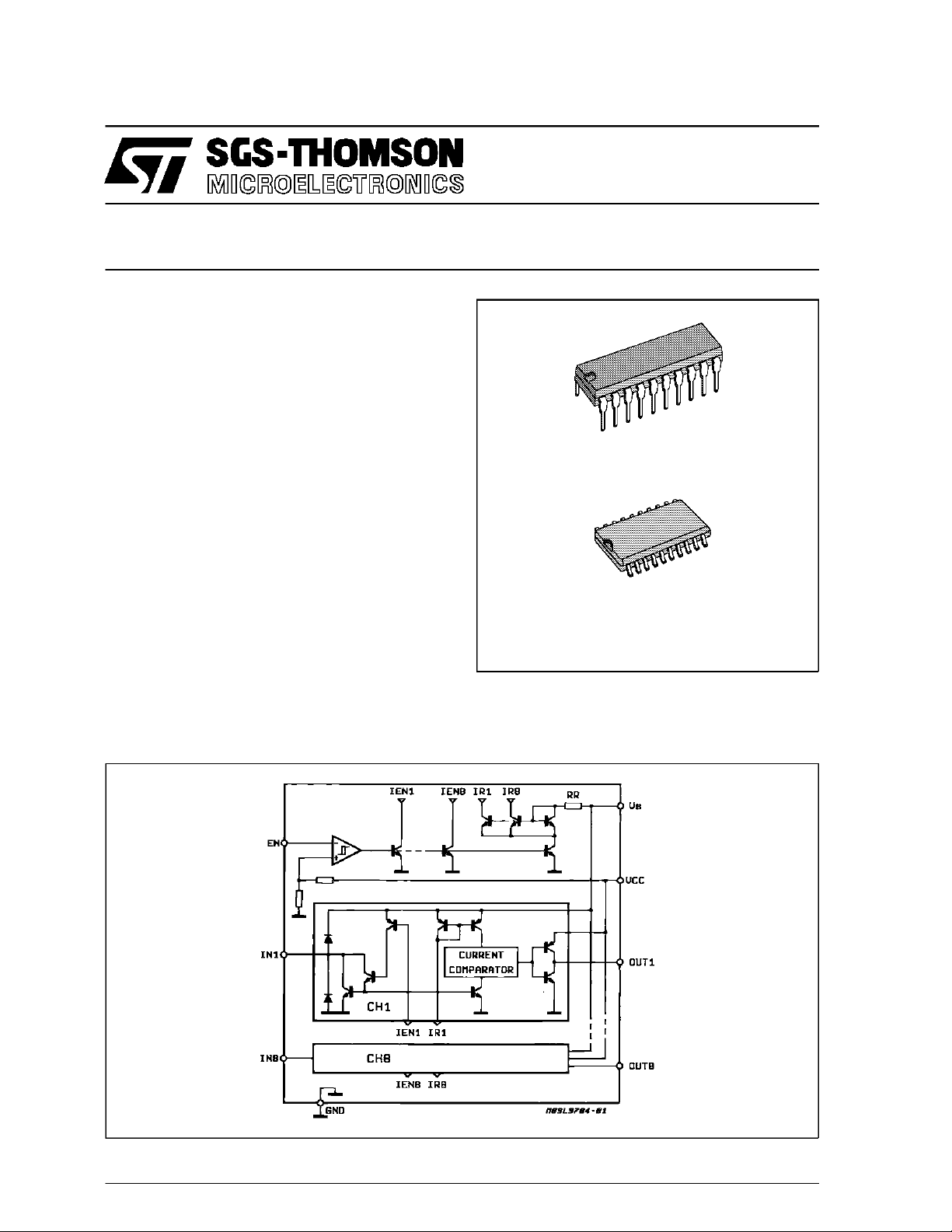
DIP–20
SO–20L
DESCRIP TIO N
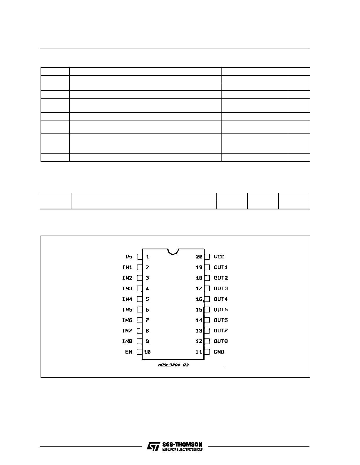
TheL9704 is a bipolarmonolithicintegratedcircuit
formonitoringthestatusofup toeightcontactsconnectedto the powersupply (battery).
BLOCK DI AG RAM
ORDERING NUMBERS: L9704 (DIP–20)
L9704D (SO–20L)
It containseight contactsenseinputsand eight microcomputercompatiblethree-stateoutputs.
March 1992
1/8
L9704
ABSOLUTE MAXIMUM RATINGS
Symbol Parameter Test Conditions Unit
V
V
I
IN DC
I
INP
I
V
P
T
stg,TJ
THERMAL DATA
Symbol Parameter DIP20 SO20 Unit
R
th j-amb
Transient Supply Voltage (t ≤ 1s) +40 V
S
Logic Supply Voltage 7 V
CC
Input DC Current ±40 mA
Input DC Pulse
(test pulse specification: 0 < tP < 2ms, f ≤ 0.2Hz, n = 25000)
Output Current Internally Limited
O
Enable Input Voltage VCC+0.3
EN
50
-75
-0.3
Power Dissipation at T
O
amb
=80°C
DIP20
SO20
875
420
Storage and Junction Temperature Range -55 to 150 °C
Thermal Resistance Junction to Ambient MAX. 80 165 °C/W
mA
mA
V
V
mW
mW
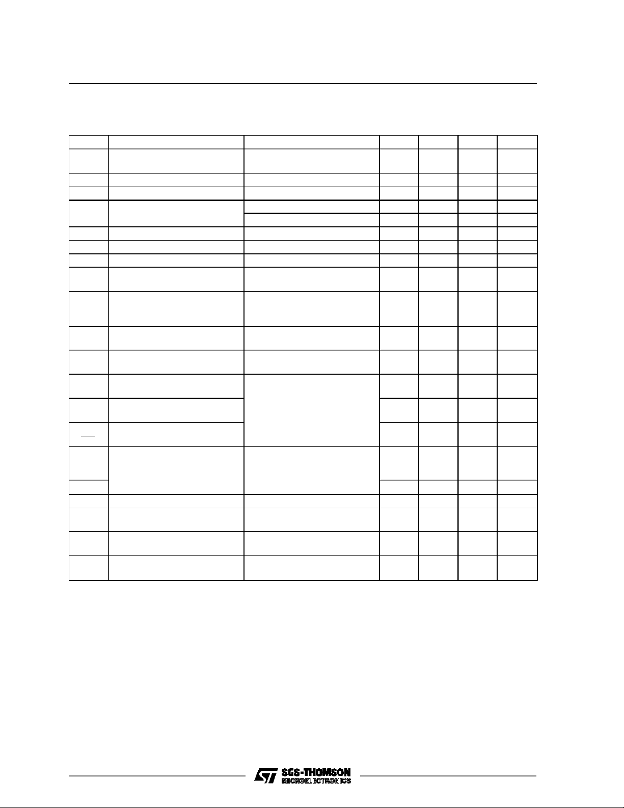
PIN CONNECTION (top view)
2/8
L9704
ELECTRICAL CHARACTERISTICS (5V ≤ VS≤ 25V; -40°C ≤ Tj≤ 125°C; 4.75V ≤ VCC≤ 5.25V unless
otherwise specified; the currents flowing in the arrow direction are assumed positive as marked in the
application circuit diagram, fig. 1).
Symbol Parameter Test Conditions Min. Typ. Max. Unit
V
Enable Input Voltage LOW
ENL
(device activated)
V
V
V
V
I
OUT TS
Enable Input Voltage HIGH 2.4 V
ENH
Enable Input Hysteresis 200 300 800 mV
ENhyst
Enable Input Current 2.4V < VEN<V
I
EN
0V < V
EN
Output Voltage HIGH 0 < I
OUTH
Output Voltage LOW I
OUTL
Output TRISTATE Current 0 < V
Input Voltage (device active) EN = LOW
V
IN
Input Voltage During Clamping
V
IN
(device disabled)
Output Current OUT = HIGH
I
OUT
Output Current OUT = LOW
I
OUT
OUT
= -1mA 0.05 0.2 0.4 V
OUT
OUT<VCC
=1kΩ
R
IN
EN = HIGH
= 30mA
I
IN
= -30mA
I
IN
=0
V
OUT
VOUT = 5.5V
Input Resistor (note 1)
R
IL
LOW Threshold
Input Resistor (note 1)
R
IH
5V < VS< 16V
∆ V
GND
HIGH Threshold
R
Input Resistor
IL
Threshold Ratio (note1)
R
IH
Quiescent Current EN = HIGH (t
I
QC
5V < V
S
-40°C ≤ T
I
QS
SI
2) Input Leakage Current All Inputs Closed V
IN
Quiescent Current EN = LOW 13
I
QC
I
QS
t
Delay Time/Output
do
All Inputs Open
C
≤ 50pF 15
OUT
(EN LOW to output data ready)
Delay Time/Tristate
t
dTS
C
≤ 50pF 10 µs
OUT
(EN HIGH to output TRISTATE)
CC
< 0.8V -5 -1 µA
< 100µA 4.0 VCC-0.1 V
0.4 1.5 2 V
V
+0.3-2VS+1-1VS+2
S
1.1 4.8 KΩ
≤ 0.1V
S
6.5 29 KΩ
0.65 0.75 0.85
ENH
≥ 80µs)
0.12 0.16 mA
< 16V
≤ 100°C
j
≤ V
BAT
D1
0.8 V
5 µA
CC
V
0.5 µA
V
-0.3
V
2mA
-20 mA
0.04 mA
0.24 mA
mA
2
mA
µs
+3R
INCIN
Notes :
1. T he input resi stor threshold value is a resist or value from t he IN–pin to battery at w hi ch the cor r es pondi ng output changes
itsstatus(seefig.3)
is the sum of the input currents SIIN=
2: SI
IN
∑
i = 1
8
I
.
IN1
3/8

L9704
APPLI CATI O N CIRCUIT DIAGRAM
Figure 1 :Typicalapplicationdiagramfor the L9704circuit.The currentflowing inthe arrow directionis as-
sumedpositive.The externalcapacitorsC
the correspondingpins.
IN
andC
representthe totalwiring capacitanceat
OUT
FUNCTIO NAL DESCRI PT I O N
TheL9704circuitmonitorsthestatusofthecontacts
connectedtobatteryandthroughtheseriesexternal
resistors R
to the contact sense input pins. The
IN
contacts equivalent circuit is supposed to be as
shown infig. 2.
The L9704 circuitcompares the input current with
the currentthrough the internalreference resistor.
Thedeviceisdesignedtoworkwithanexternalinput
seriesresistorofR
=1kΩ.Withthisinputresistor
IN1-8
the contactcurrent,when thecontactis closedand
the deviceactivated (EN= LOW) is
+∆V
V
BAT
=
I
IN
1KΩ (1)
Forthis calculationthelimitvalueofthe V
BAT
–2V
(satura-
IN
tionvoltageof 2V)was consideredsothatthelowest
limit value ofI
iscalculatedin (1).
IN
Thefunctionof thecircuitcan bedemonstratedwith
the transfer characteristics, showing the output
4/8
status as a functionof the input resistorR
in figure3. Theinputresistorisa sumoftheR
the contactresistanceR
CON
orR
COFF
, shown
I
and
IN
, fortheclosed
contact:
R
I=RIN+RCON
, (2)
and fortheopen contact:
R
I=RIN+RCOFF
. (3)
TheoutputgoesHIGHwhentheinputresistanceincreasesabove6.5kΩ(typicalvalue)andgoesLOW,
when the inputresistancedecreasesbelow 4.8KΩ
(typical value). The limit values of R
LOW andR
withR
=29kΩ forHIGHimpliesthat acontact
I
=100Ω(atIIN=10mA)will berecognized
CON
as ON= LOWand acontactwithR
= 1.1KΩ for
I
=28kΩwill
COFF
be recognized as OFF = HIGH. These limits are
validwithinthesupplyvoltagerange5V≤ V
≤ 16V,
s
the battery voltage potential difference of
∆VBAT≤0.1V
andthevariationofthereverse
BAT
batteryprotectiondiodeD1voltagefrom0.5V to1V.

L9704
Theinternalclampingdiodesatthecontactmonitoringinputs, togetherwiththe externalcontactseries
resistors R
, allows the device to withstand tran-
IN
sientsatthe contactconnection.Thecontactseries
resistorR
limitsthe input currentat the transient.
IN
The dynamic behaviourof the circuit is definedby
the times t
open, the input capacitor C
do
andt
. Whenthe contact becomes
dTS
must be charged
IN
throughthe resistorR
. In this casethe total delay
IN
timemay alsobeinfluencedbythetimeconstantR
CIN. The delaytime t
, whendisabling thedevice
dTS
isdefinedonlybytheinternalcircuitry. Inbothcases,
anexternaloutputcapacitancelessthan50pFisassumed, the internal output capacitances of the
three-statebuffers areless than5pF.
Figure 2 : The ContactSenseInput Connectionwith theContact EquivalentCircuit.
IN
Figure 3 : The OutputVoltageas a Functionof the InputResistanceat the CorrespondingContact Sense
Input.
5/8

L9704
SO20 PACKAGE MECHANICAL DATA
DIM.
MIN. TYP. MAX. MIN. TYP. MAX.
A 2.65 0.104
a1 0.1 0.3 0.004 0.012
a2 2.45 0.096
b 0.35 0.49 0.014 0.019
b1 0.23 0.32 0.009 0.013
C 0.5 0.020
c1 45 (typ.)
D 12.6 13.0 0.496 0.512
E 10 10.65 0.394 0.419
e 1.27 0.050
e3 11.43 0.450
F 7.4 7.6 0.291 0.299
L 0.5 1.27 0.020 0.050
M 0.75 0.030
S 8 (max.)
mm inch
6/8

DIP20 PACKAGE MECHANICAL DATA
L9704
DIM.
MIN. TYP. MAX. MIN. TYP. MAX.
a1 0.254 0.010
B 1.39 1.65 0.055 0.065
b 0.45 0.018
b1 0.25 0.010
D 25.4 1.000
E 8.5 0.335
e 2.54 0.100
e3 22.86 0.900
F 7.1 0.280
I 3.93 0.155
L 3.3 0.130
Z 1.34 0.053
mm inch
7/8

L9704
Information furnished is believed to be accurate and reliable. However, SGS-THOMSON Microelectronics assumes no responsibility for
the consequences of use of such information nor for any infringement of patents or other rights of third parties which may result from its
use. No license is granted by implication or otherwise under any patent or patent rights of SGS-THOMSON Microelectronics. Specifications mentioned in this publication are subject to change without notice. This publication supersedes and replaces all information previously supplied. SGS-THOMSON Microelectronics products are not authorized for use as critical components in life support devices or
systems without express written approval of SGS-THOMSON Microelectronics.
1994 SGS-THOMSON Microelectronics - All Rights Reserved
Australia - Brazil - France - Germany - Hong Kong - Italy - Japan - Korea - Malaysia - Malta - Morocco - The Netherlands - Singapore-
SGS-THOMSON Microelectronics GROUP OF COMPANIES
Spain - Sweden - Switzerland - Taiwan - Thaliand - United Kingdom - U.S.A.
8/8
 Loading...