

OCTALSUPPLY CONTACTMONITORINGCIRCUIT
.OPERATING DC SUPPLY VOLTAGE RANGE
5V TO25V
.SUPPLYOVERVOLTAGEPULSEUP TO 40V
.VERY LOW STANDBY QUIESCENT CUR-
RENT0.2mA
.INTERNAL CLAMPINGDIODESAT CONTACT
INPUTS TO V
ANDGND
S
.INPUT PULSECURRENTCAPABILITYUP TO
+ 50mA,– 75mA
.NOMINAL CONTACT CURRENTS OF 10mA
DEFINED BY EXTERNAL CONTACT SERIES
RESISTORSR
IN1-8
.CONTACT STATUS MONITORING BY COM-
PARING THE RESISTANCE AT CONTACT
SENSEINPUTSWITHTHEINTERNALREFERENCERESISTORVALUE
.HIGH IMMUNITYDUETORESISTANCECOM-
PARISONWITH HYSTERESIS
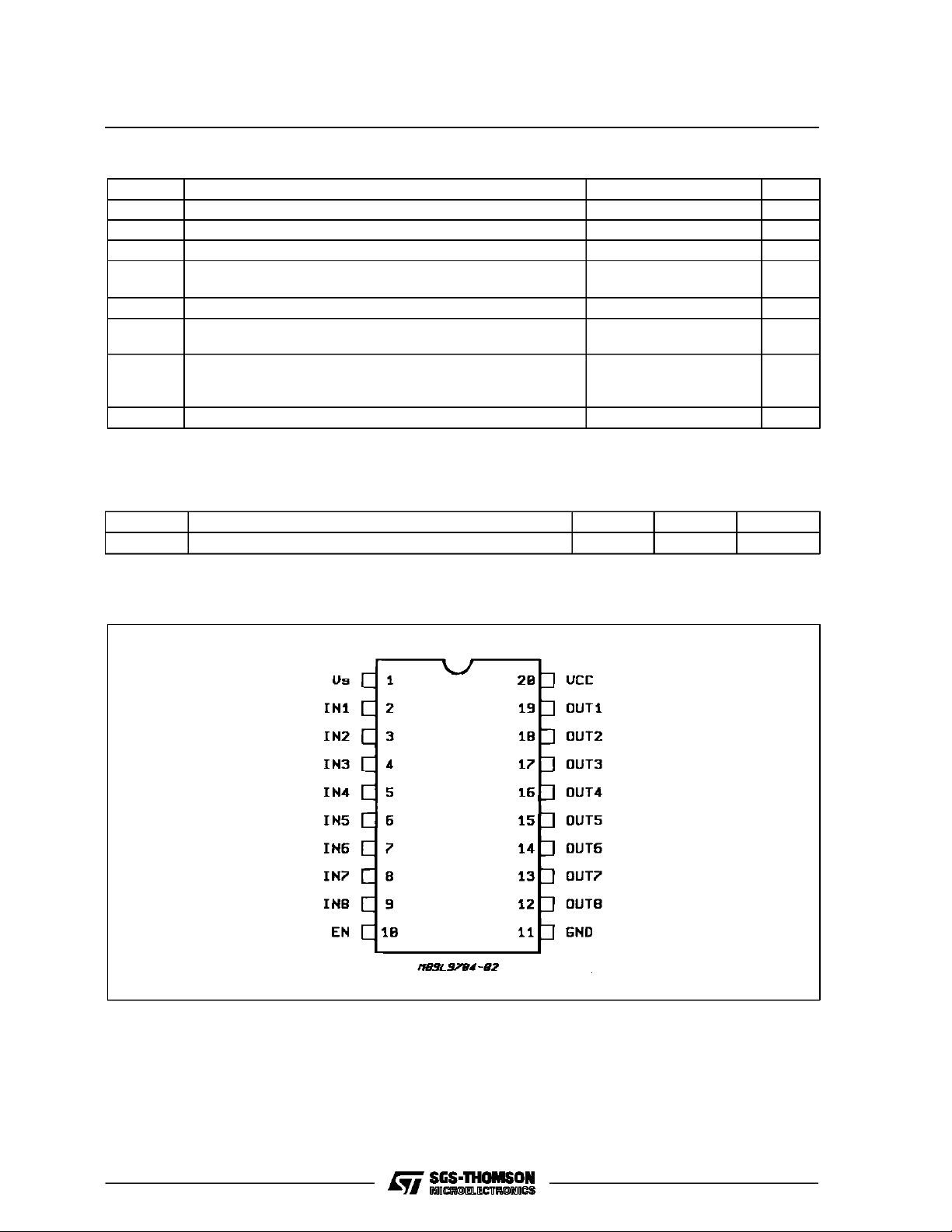
L9704
DIP–20
SO–20L
DESCRIP TIO N
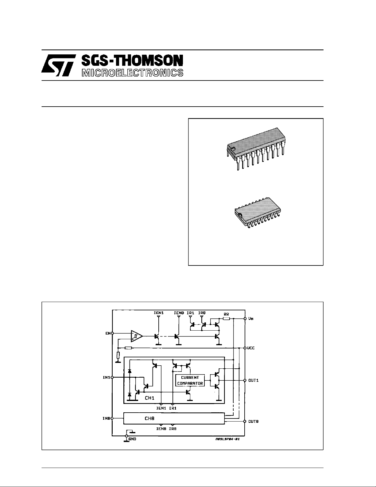
TheL9704 is a bipolarmonolithicintegratedcircuit
formonitoringthestatusofup toeightcontactsconnectedto the powersupply (battery).
BLOCK DI AG RAM
ORDERING NUMBERS: L9704 (DIP–20)
L9704D (SO–20L)
It containseight contactsenseinputsand eight microcomputercompatiblethree-stateoutputs.
March 1992
1/8
L9704
ABSOLUTE MAXIMUM RATINGS
Symbol Parameter Test Conditions Unit
V
V
I
IN DC
I
INP
I
V
P
T
stg,TJ
THERMAL DATA
Symbol Parameter DIP20 SO20 Unit
R
th j-amb
Transient Supply Voltage (t ≤ 1s) +40 V
S
Logic Supply Voltage 7 V
CC
Input DC Current ±40 mA
Input DC Pulse
(test pulse specification: 0 < tP < 2ms, f ≤ 0.2Hz, n = 25000)
Output Current Internally Limited
O
Enable Input Voltage VCC+0.3
EN
50
-75
-0.3
Power Dissipation at T
O
amb
=80°C
DIP20
SO20
875
420
Storage and Junction Temperature Range -55 to 150 °C
Thermal Resistance Junction to Ambient MAX. 80 165 °C/W
mA
mA
V
V
mW
mW
PIN CONNECTION (top view)
2/8
L9704
ELECTRICAL CHARACTERISTICS (5V ≤ VS≤ 25V; -40°C ≤ Tj≤ 125°C; 4.75V ≤ VCC≤ 5.25V unless
otherwise specified; the currents flowing in the arrow direction are assumed positive as marked in the
application circuit diagram, fig. 1).
Symbol Parameter Test Conditions Min. Typ. Max. Unit
V
Enable Input Voltage LOW
ENL
(device activated)
V
V
V
V
I
OUT TS
Enable Input Voltage HIGH 2.4 V
ENH
Enable Input Hysteresis 200 300 800 mV
ENhyst
Enable Input Current 2.4V < VEN<V
I
EN
0V < V
EN
Output Voltage HIGH 0 < I
OUTH
Output Voltage LOW I
OUTL
Output TRISTATE Current 0 < V
Input Voltage (device active) EN = LOW
V
IN
Input Voltage During Clamping
V
IN
(device disabled)
Output Current OUT = HIGH
I
OUT
Output Current OUT = LOW
I
OUT
OUT
= -1mA 0.05 0.2 0.4 V
OUT
OUT<VCC
=1kΩ
R
IN
EN = HIGH
= 30mA
I
IN
= -30mA
I
IN
=0
V
OUT
VOUT = 5.5V
Input Resistor (note 1)
R
IL
LOW Threshold
Input Resistor (note 1)
R
IH
5V < VS< 16V
∆ V
GND
HIGH Threshold
R
Input Resistor
IL
Threshold Ratio (note1)
R
IH
Quiescent Current EN = HIGH (t
I
QC
5V < V
S
-40°C ≤ T
I
QS
SI
2) Input Leakage Current All Inputs Closed V
IN
Quiescent Current EN = LOW 13
I
QC
I
QS
t
Delay Time/Output
do
All Inputs Open
C
≤ 50pF 15
OUT
(EN LOW to output data ready)
Delay Time/Tristate
t
dTS
C
≤ 50pF 10 µs
OUT
(EN HIGH to output TRISTATE)
CC
< 0.8V -5 -1 µA
< 100µA 4.0 VCC-0.1 V
0.4 1.5 2 V
V
+0.3-2VS+1-1VS+2
S
1.1 4.8 KΩ
≤ 0.1V
S
6.5 29 KΩ
0.65 0.75 0.85
ENH
≥ 80µs)
0.12 0.16 mA
< 16V
≤ 100°C
j
≤ V
BAT
D1
0.8 V
5 µA
CC
V
0.5 µA
V
-0.3
V
2mA
-20 mA
0.04 mA
0.24 mA
mA
2
mA
µs
+3R
INCIN
Notes :
1. T he input resi stor threshold value is a resist or value from t he IN–pin to battery at w hi ch the cor r es pondi ng output changes
itsstatus(seefig.3)
is the sum of the input currents SIIN=
2: SI
IN
∑
i = 1
8
I
.
IN1
3/8
 Loading...