

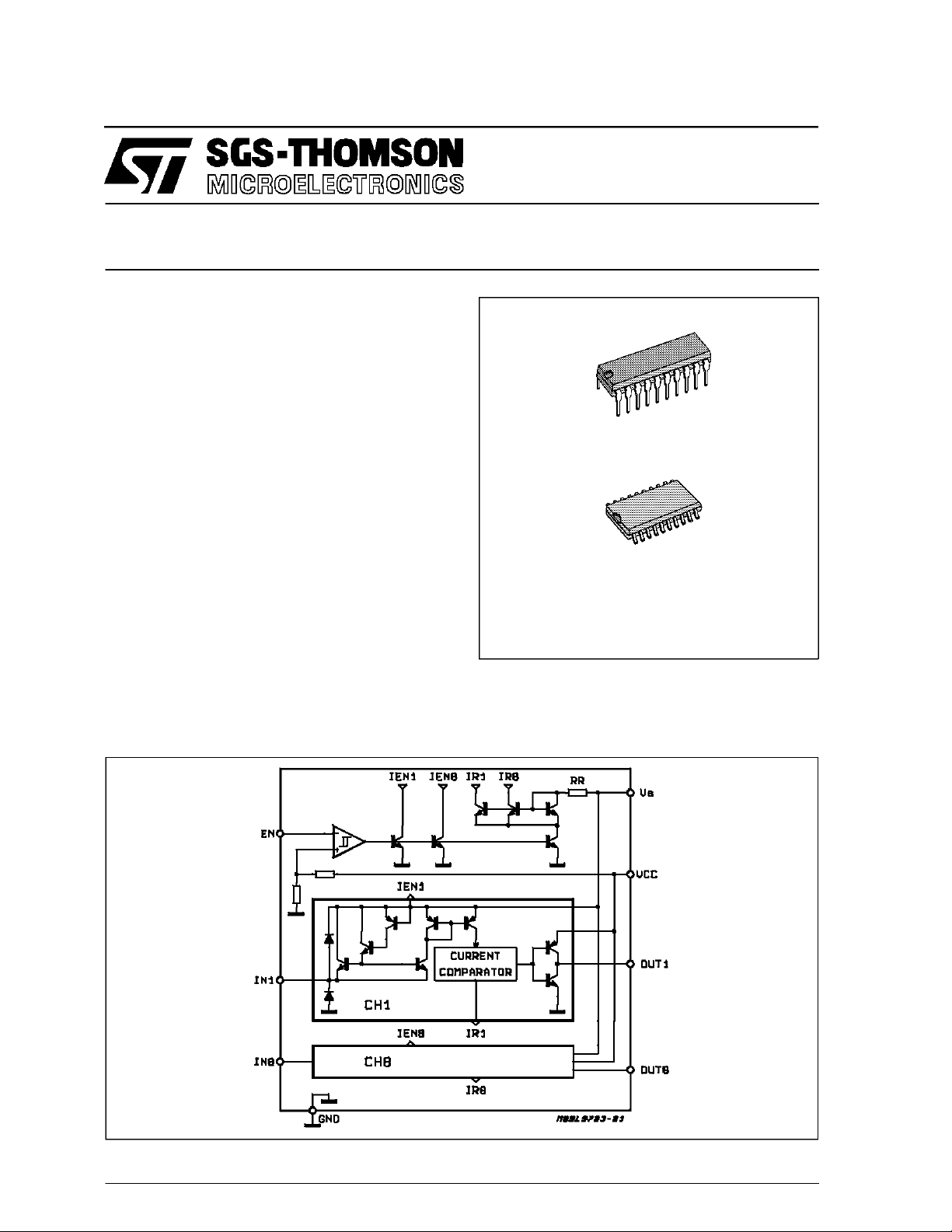
OCTAL GROUND CONTACT MONITORING CIRCUIT
.OPERATING DC SUPPLY VOLTAGE RANGE
5V TO 25V
.SUPPLYOVERVOLTAGEPULSEUP TO 40V
.VERY LOW STANDBY QUIESCENT CUR-
RENT0.2mA
.INTERNAL CLAMPING DIODESATCONTACT
INPUTS TO V
ANDGND
S
.INPUTPULSECURRENT CAPABILITYUPTO
+ 50mA ;– 75mA
.NOMINALCONTACTCURRENT OF10mADE-
FINEDBYEXTERNALCONTACT SERIESRESISTORS R
I N1–8
.CONTACT STATUS MONITORING BY COM-
PARING THE RESISTANCE AT CONTACT
SENSEINPUTSWITHTHEINTERNALREFERENCERESISTOR VALUE
.HIGHIMMUNITYDUETORESISTANCECOM-
PARISONWITH HYSTERESIS
L9703
DIP-20
SO-20L
ORDERINGNUMBERS : L9703 (DIP-20)
L9703D (SO-20L)
DESCRIPTION
TheL9703isa bipolarmonolithicintegratedcircuitfor monitoringthe statusofupto eightcontactsconnectedto GND.
BLOCK DIAGRAM
It containseightcontactsenseinputsandeight
microcomputercompatiblethree-stateoutputs.
March 1992
1/9
L9703
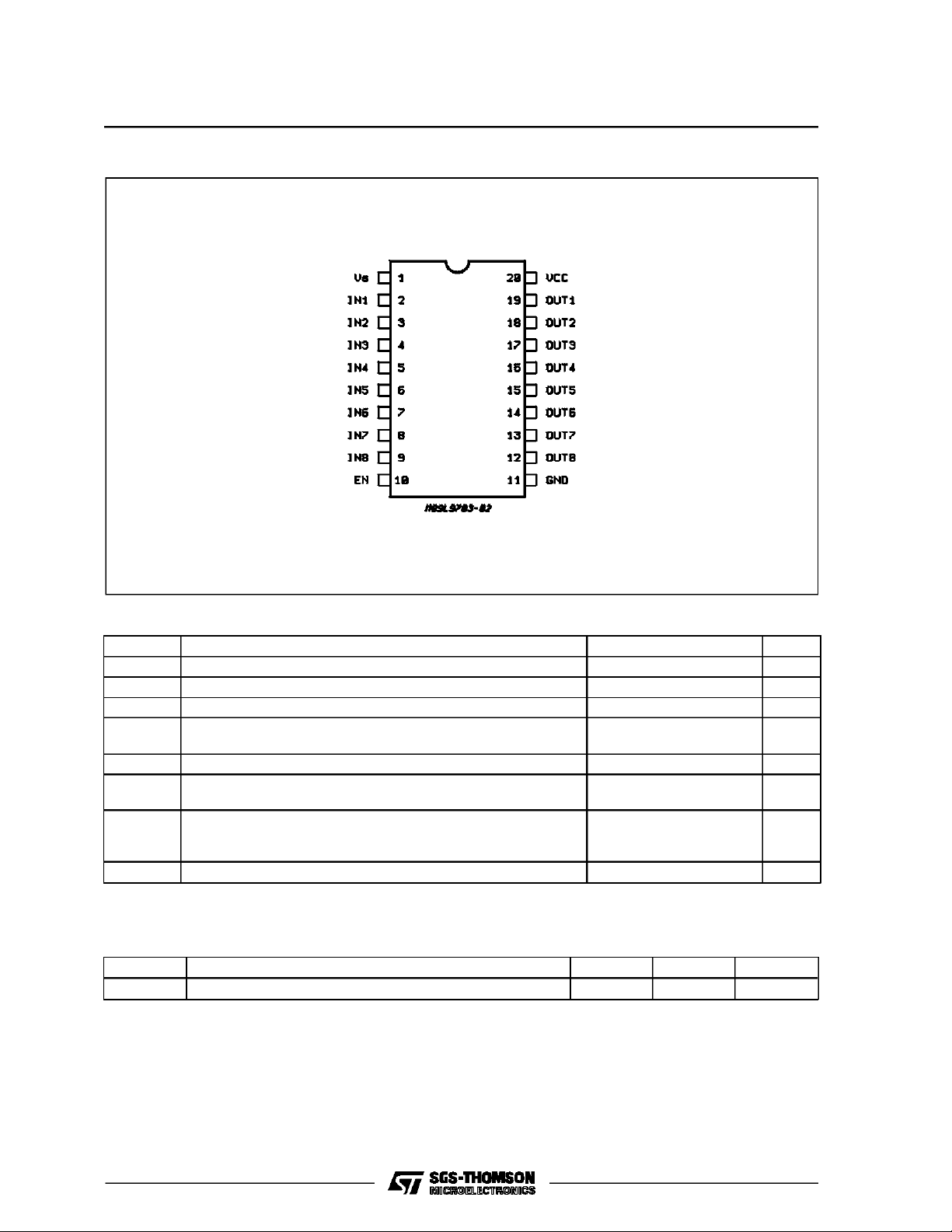
PIN CONNECTION (top view)
ABSOLUTE MAXIMUM RATINGS
Symbol Parameter Test Conditions Unit
V
V
I
IN DC
I
INP
I
V
CC
O
EN
Transient Supply Voltage (t ≤ 1s) +40 V
S
Logic Supply Voltage 7 V
Input DC Current ±40 mA
Input DC Pulse
(test pulse specification: 0 < tP < 2ms, f ≤ 0.2Hz, n = 25000)
50
-75
Output Current Internally Limited
Enable Input Voltage VCC+0.3
-0.3
T
P
O
stg,TJ
Power Dissipation at T
amb
=80°C
DIP20
SO20
875
420
Storage and Junction Temperature Range -55 to 150 °C
THERMAL DATA
Symbol Parameter DIP20 SO20 Unit
R
th j-amb
Thermal Resistance Junction to Ambient MAX. 80 165 °C/W
mA
mA
V
V
mW
mW
2/9
L9703
ELECTRICALCHARACTERISTICS (5V ≤ VS≤ 25V; -40°C ≤ Tj≤ 125°C;4.75V ≤ VCC≤ 5.25Vunless oth-
erwise specified;thecurrentsflowinginthearrowdirectionareassumedpositiveas markedintheapplication
circuitdiagram,fig. 1).
Symbol Parameter Test Conditions Min. Typ. Max. Unit
V
ENL
V
ENH
V
ENhyst
I
EN
V
OUTH
V
OUTL
I
OUT TS
V
IN
V
IN
I
OUT
I
OUT
R
IL
R
IH
R
IL
R
IH
I
QC
I
QS
I
QC
I
QS
t
do
t
dTS
Enable Input Voltage LOW
(device activated)
Enable Input Voltage HIGH 2.4 V
Enable Input Hysteresis 200 420 800 mV
Enable Input Current 2.4V < VEN<V
0V < V
EN
Output Voltage HIGH 0 < I
Output Voltage LOW I
Output TRISTATE Current 0 < V
OUT
= -1mA 0.05 0.2 0.4 V
OUT
OUT<VCC
CC
< 0.8V -5 -1 µA
< 100µA 4.0 VCC-0.1 V
Input Voltage (device active) EN = LOW
=1kΩ
R
Input Clamped Voltage
(device disabled)
IN
EN = HIGH
= 30mA
I
IN
= -30mA
I
IN
-2 VS-1.5 VS- 0.4 V
V
S
V
+0.3-2VS+1-1VS+2
S
Output Current OUT = HIGH
=0
V
OUT
Output Current OUT = LOW
VOUT = 5.5V
Input Resistor (note 1)
LOW Threshold
Input Resistor (note 1)
5V < VS< 16V
GND
≤ 0.1V
∆ V
S
1.8 4 KΩ
5.3 20 KΩ
HIGH Threshold
Input Resistor
0.65 0.75 0.85
Threshold Ratio (note1)
Quiescent Current EN = HIGH (t
5V < V
-40°C ≤ T
< 16V
S
ENH
≤ 100°C
j
≥ 80µs)
0.12 0.16 mA
Quiescent Current All Inputs Open 0.04 mA
All Inputs Closed 0.24 mA
Quiescent Current EN = LOW 6
Delay Time/Output
(EN LOW to output data ready)
Delay Time/Tristate
(EN HIGH to output TRISTATE)
C
≤ 50pF 15
OUT
C
≤ 50pF 10 µs
OUT
0.8 V
5 µA
CC
V
0.5 µA
V
-0.3
V
2mA
-20 mA
mA
6
mA
µs
+3R
INCIN
Note : 1. The input resistor threshold value is theresistor value from theIN-pin to ground at which the corresponding output changes
itsstatus (see fig. 3).
3/9

L9703
APPLICATION CIRCUIT
Figure 1 : TypicalApplicationDiagram for the L9703Circuit.The currentflowingin the arrowdirection is
assumedpositive.TheexternalcapacitorsC
at the correspondingpins.
IN
andC
representthe total wiring capacitance
OUT
4/9

FUNCTIONAL DESCRIPTION
TheL9703circuitmonitorsthestatusofthecontacts
connectedtoground and throughthisseries externalresistorsR
tothecontactsenseinputpins.The
IN
contacts equivalent circuit is supposed to be as
shownin fig.2.
The L9703 circuit compares the input current with
the current through the internalreference resistor.
Thedeviceisdesignedtoworkwithanexternalinput
seriesresistorofR
=1kΩ.Withthisinputresistor
IN1-8
the contact current,when the contactisclosed and
the device activated(EN = LOW)is
-2V
V
S
=
I
IN
1kΩ (1)
For this calculation the limit value of the V
S
to IN
saturationvoltageof2V wasconsideredso thatthe
lowestlimitvalue of I
iscalculatedin(1).
IN
Thefunctionof thecircuitcanbedemonstratedwith
the transfer characteristics, showing the output
statusas a functionof the input resistor R
infigure3.Theinputresistorisasum of theR
thecontactresistanceR
CON
orR
COFF
, shown
I
and
IN
, fortheclosed
contact:
R
I=RIN+RCON,
(2)
and for theopen contact:
R
I=RIN+RCOFF
. (3)
L9703
TheoutputgoesHIGHwhentheinputresistanceincreasesabove5.3kΩ(typicalvalue)andgoesLOW,
when the input resistance decreases below 4kΩ
(typical value). The limit values of R
LOWandR
withR
=20kΩ forHIGHimpliesthat a contact
I
=100Ω (atIIN=10mA)will berecognized
CON
as ON=LOW anda contactwithR
be recognized as OFF = HIGH. These limits are
validwithin the supplyvoltagerange6V ≤ VS≤ 16V
and the ground potential difference of
∆VGND = 0,1V.
The internalclampingdiodes at the contact monitoringinputs,togetherwiththeexternalcontactsseries resistors R
, allows the device to withstand
IN
transientsatthecontactconnection.Thecontactseriesresistor R
limits the input current at the tran-
IN
sient.
The dynamicbehaviour of the circuit is definedby
the timest
do
andt
inputcapacitorC
sistorR
. In this casethe totaldelaytimemay also
IN
. Whenthe contactisopen,the
dTs
mustbe chargedthroughthe re-
IN
be influencedby the timeconstantR
Thedelaytimet
,whendisablingthedevice,isde-
dTs
finedonlyby the internalcircuitry. Inboth cases,an
external output capacitanceless than 50pF is assumed, the internal output capacitances of the
three-statebuffers are less than5pF.
= 1.8KΩ for
I
=19kΩwill
COFF
INCIN
.
Figure 2 : The Contact SenseInputConnectionwith the ContactEquivalentCircuit.
5/9

L9703
Figure 3 : The OutputVoltageas a Functionof theInput Resistanceat the CorrespondingContact Sense
Input.
6/9

SO20 PACKAGE MECHANICAL DATA
L9703
DIM.
MIN. TYP. MAX. MIN. TYP. MAX.
A 2.65 0.104
a1 0.1 0.3 0.004 0.012
a2 2.45 0.096
b 0.35 0.49 0.014 0.019
b1 0.23 0.32 0.009 0.013
C 0.5 0.020
c1 45 (typ.)
D 12.6 13.0 0.496 0.512
E 10 10.65 0.394 0.419
e 1.27 0.050
e3 11.43 0.450
F 7.4 7.6 0.291 0.299
L 0.5 1.27 0.020 0.050
M 0.75 0.030
S 8 (max.)
mm inch
7/9

L9703
DIP20 PACKAGE MECHANICAL DATA
DIM.
MIN. TYP. MAX. MIN. TYP. MAX.
a1 0.254 0.010
B 1.39 1.65 0.055 0.065
b 0.45 0.018
b1 0.25 0.010
D 25.4 1.000
E 8.5 0.335
e 2.54 0.100
e3 22.86 0.900
F 7.1 0.280
I 3.93 0.155
L 3.3 0.130
Z 1.34 0.053
mm inch
8/9

L9703
Information furnished is believed to be accurate and reliable. However, SGS-THOMSON Microelectronics assumes no responsibility for
the consequences of use of such information nor for any infringement of patents or other rights of third parties which may result from its
use. No license is granted by implication or otherwise under any patent or patent rights of SGS-THOMSON Microelectronics. Specifications mentioned in this publication are subject to change without notice. This publication supersedes and replaces all information previously supplied. SGS-THOMSON Microelectronics products are not authorized for use as critical components in life support devices or
systems without express written approval of SGS-THOMSON Microelectronics.
1994 SGS-THOMSON Microelectronics - All Rights Reserved
SGS-THOMSON Microelectronics GROUP OF COMPANIES
Australia - Brazil - France - Germany - Hong Kong - Italy - Japan - Korea - Malaysia - Malta - Morocco - The Netherlands - Singapore-
Spain - Sweden - Switzerland - Taiwan - Thaliand - United Kingdom - U.S.A.
9/9
 Loading...