

.HIGH PERFORMANCE CLAMPING AT
GROUND ANDPOSITIVEREFERENCE
VOLTAGE
.FASTACTIVECLAMPING
.OPERATINGRANGE4.75- 5.25V
.SINGLEVOLTAGEFORSUPPLYANDPOSITI-
VEREFERENCE
.LOW QUIESCENTCURRENT
.LOW INPUT LEAKAGECURRENT
DESCRI P TI ON
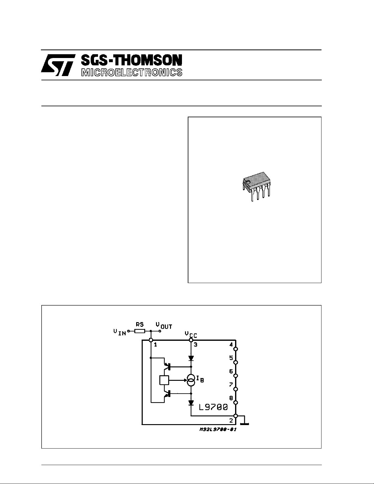
TheL9700isa monolithiccircuitwhichis suited for
input protectionand voltageclampingpurpose.
The limiting function is referred to ground and the
positivesupplyvoltage.
Onesingleelementcontainssix independentchannels.
Very fast speed is achieved by internal feedback
and the applicationofa new vertical PNP-transistor
with isolatedcollector.
L9700
HEX PRECISION LIMITER
Minid i p
ORDE R I N G NUMBE R : L9700
BLOCK DIAGRAM
November 1990
This is advanced informationon a newproduct now in development or undergoing evaluation. Detailsare subject to change withoutnotice.
1/5
L9700
ABSOLUTE MAXIMUM RATINGS
Symb o l Para met er Value Unit
V
T
j,Tstg
Note: Thecircuitis ESDprotected according to MIL-STD-883C
THERMAL DATA
Symb o l Para met er Value Unit
R
thj-amb
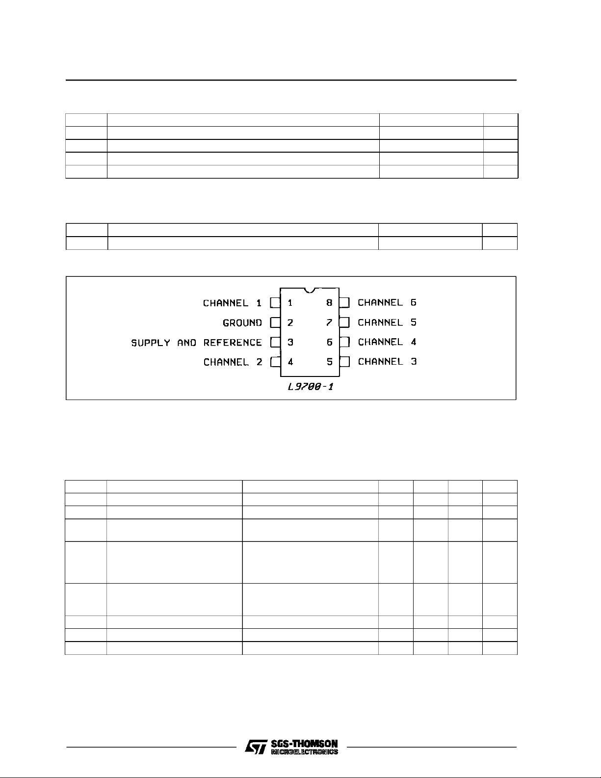
PI N CONNECTION
SupplyVoltage 20 V
CC
InputCurrent per Channel 30 mA
I
IN
Junctionand StorageTemperature –55 to 150 °C
TotalPower Dissipation (T
P
tot
=85°C) 650 mW
amb
Thermal Resistance Junction to Ambient Max. 100 °C/W
ELECTRICAL CHARACTERISTICS (VCC= 5V, TJ= –40 to 125°C unless otherwise specified)
Symb o l Parameter Test condi t ion Mi n . Typ . Max. Unit
V
V
V
cld
t
S
R
C
(*) Design limits are guaranteed by statistical control on production samples over the indicated temperature and supply voltage
ranges. These limits are not used to calculate outgoing quality levels.
2/7
SupplyVoltage 4.75 5.25 V
CC
SupplyCurrent 1.5 3 mA
I
CC
Static InputClamping Voltage Negative IIN=–10mA
cis
PositiveI
Input Current (static) VIN=0
I
IN
V
IN=VCC
VIN= 50mV
V
IN=VCC
= +10mA
IN
–50mV
–250
V
CC
0
V
+2 50
CC
15
15
5
5
(*) Dynamic Input Clamping Voltage IIN= ± 10mA, tR=5ns
PositiveOvershoot
Negative Overshoot
400
400
(*) SettingTime See fig.2 20 ns
(*) Dynamic Input Resistance 5 Ω
IN
(*) Crosstalkbetween any two inputs 0 ≤ VIN≤ VCC,fIN< 1kHz 70 dB
rtk
mV
µA
µA
µA
µA
mV
mV
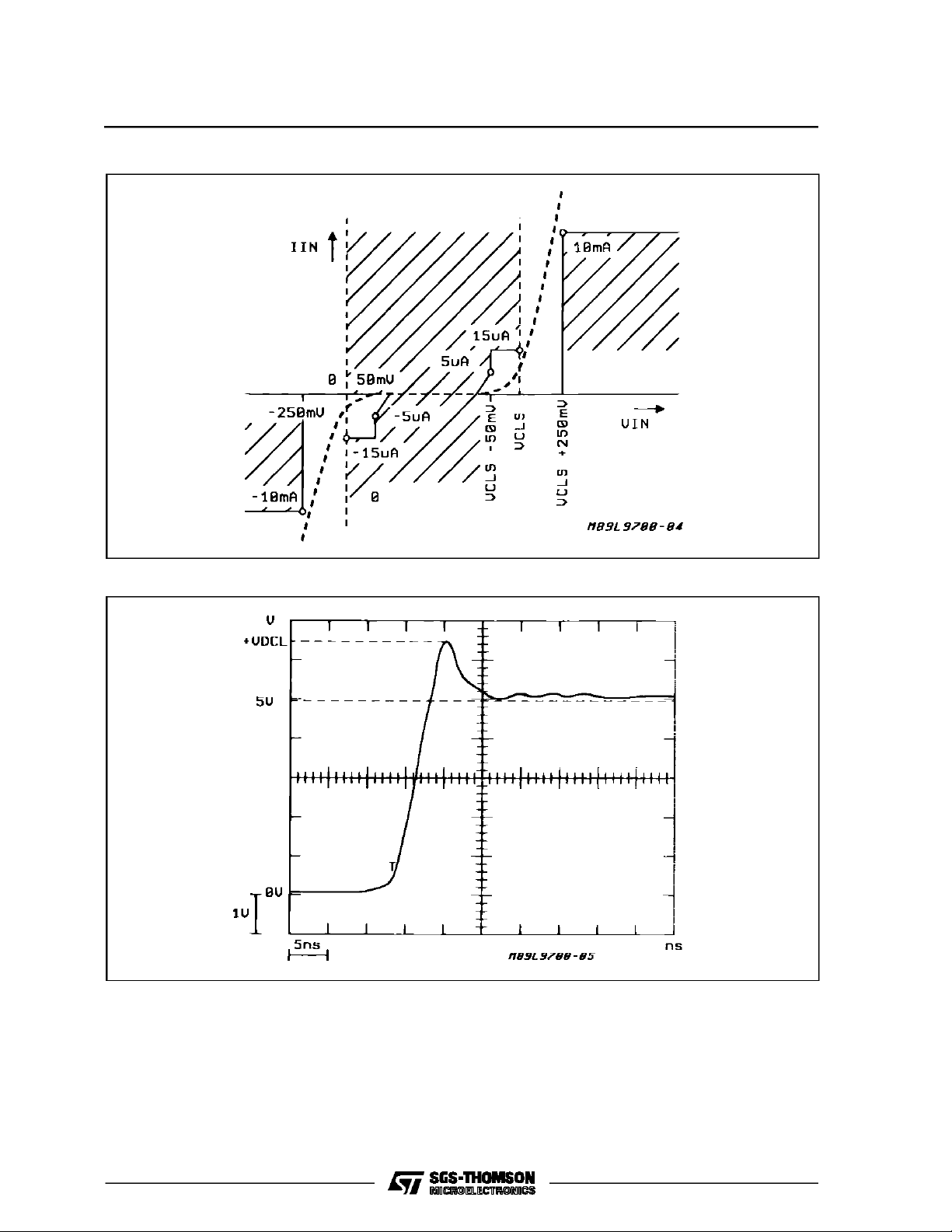
Figure1 : DC INPUTCHARACTERISTIC Limit Points of the CharacteristicApproximation.
L9700
Figure2 : DynamicalInputCharacteristics.
2a
3/7

L9700
Figure2 : DynamicalInputCharacteristics (continued).
2b
APPLI CATI ON INFORMATION
Mostintegratedcircuits, bothHNMOSand bipolar,
are very sensitivetopositive and negativeovervoltageson the supplyand atthe inputs.
These transients occur in large numbers and with
different magnitudes in the automotive environment, making adequate protection for devices aimed at it indispensible.
Overvoltageson the supply line are facedthrough
high voltage integrationtechnologiesorthroughexternalprotection(transil, varistor).
Signalinputsaregenerallyprotectedusingclampdiodestothesupplyandground,andacurrentlimi-ter
resistor. However, such solutions do not always
completely satisfy the protection specifications in
termsofinterventionspeed,negativeclamping and
current leakage high enough to change analog signals.
The L9700 device combines a high intervention
speed with a high precision positive and negative
clamp anda lowcurrent leakageprovidingthe optimalsolutionto the problems of the automotiveenvironment.
Thehighintervention speed, due to the pre-bias of
the limiter stage and internal feedback, limits the
voltageovershootandavoidthe use of externalcapacitorsfor thelimitation of thetransient rise times.
Figure3 illustratesa typicalautomotiveapplication
scheme.The resistor R
limits the input current of
S
the device and is thereforedimensionedconsideringthe characteristicsof the transients to be eliminated.Consequently:
V
RS=
transientPeak
I
IN MAX
TheCINcapacitorsmust be used onlyonanalog inputsbecausetheypresenta low impedanceduring
thesampling period.
4/7

Figure3 : TypicalApplication.
L9700
The minimum valuefor C
isdeterminedby theac-
IN
curacyrequired,the timetakentosamplethe input
and theinputimpedance duringthat time,while the
maximum value is determinedby the requiredfrequencyresponseandthe valueof R
.
S
Thusfor a resistive inputA/D connectorwhere :
T
= Sampletime(Seconds)
S
R
= Deviceinputresistance(Ohms)
D
V
= Inputvoltage(Volts)
IN
k = Requiredaccuracy(%)
Q
= Chargeon capacitor beforesampling
1
Q
= Chargeon capacitor aftersampling
2
I
= Deviceinputcurrent (Amps)
D
Thus:
k ⋅ Q
Q1–Q2=
1
100
but Q
and Q1–Q2=ID–T
so that IDTS=
and CIN(min) = Farad
so CIN(min) = Farad
1=CINVIN
k⋅CIN–V
S
100
⋅ T
I
D
V
IN
100 ⋅ T
k ⋅ R
IN
S
⋅ k
S
D
Thecalculationforasampleandholdtypeconvertor
is even simpler :
k = Requiredaccuracy(%)
C
= Hold capacitor(Farad)
H
CIN(min) = Farad
100⋅ C
H
k
5/7

L9700
MINIDIP PACKAGE MECHANICAL DATA
DIM.
MIN. TYP. MAX. MIN. TYP. MAX.
A 3.32 0.131
a1 0.51 0.020
B 1.15 1.65 0.045 0.065
b 0.356 0.55 0.014 0.022
b1 0.204 0.304 0.008 0.012
D 10.92 0.430
E 7.95 9.75 0.313 0.384
e 2.54 0.100
e3 7.62 0.300
e4 7.62 0.300
F 6.6 0.260
I 5.08 0.200
L 3.18 3.81 0.125 0.150
Z 1.52 0.060
mm inch
6/7

L9700
Information furnished is believed to be accurate and reliable. However, SGS-THOMSON Microelectronics assumes no responsibility for
the consequences of use of such information nor for any infringement of patents or other rights of third parties which may result from its
use. No license is granted by implication or otherwise under any patent or patent rights of SGS-THOMSON Microelectronics. Specifications mentioned in this publication are subject to change without notice. This publication supersedes and replaces all information previously supplied. SGS-THOMSON Microelectronics products are not authorized for use as critical components in life support devices or
systems without express written approval of SGS-THOMSON Microelectronics.
1994 SGS-THOMSON Microelectronics - All Rights Reserved
Australia - Brazil - France - Germany - Hong Kong - Italy - Japan - Korea - Malaysia - Malta - Morocco - The Netherlands - Singapore -
SGS-THOMSON Microelectronics GROUP OF COMPANIES
Spain - Sweden - Switzerland - Taiwan - Thaliand - United Kingdom - U.S.A.
7/7
 Loading...