

FAULT TOLERANT CAN TRANSCEIVER
■ FAULT TOLERANT DIFFERENTIAL
CAN TRANSCEIVER
■ OPERATING SUPPLY VO LT AG E 6V TO 28V,
TRANSIENTS UP TO 40V
■ LOW QUIESCENT CURRENT IN STANDBY
MODE (100
■ ON CHIP DIAGNOSIS FO R ERRORS ON THE
PHYSICAL BUSLINES WITH MICRO
CONTROLLER INTERFACE
■
OPTIMIZED EMI BEHAVIOUR DUE TO LIMITED
AND SYMM ETRIC SLOPES OF CAN SIGNALS
■ AUTOMATIC SWITCHING TO SINGLE WIRE
MODE UPON BUS FAILURES
■ TWO-EDGE SENSITIVE WAKE-UP PIN
■ SUPPORTS TRANSMISS ION WITH G ROUND
SHIFT VOLTAGES:
SINGLE WIRE: 1.5V
DIFFERENTIAL WIRE: 3v
■ AN UNPOWERED NODE OR UNSUFFICIENT
µA) AND SLEEP MOD E (37 µ A)
L9669
SO14
ORDERING NUMBER: L9669
SUPPLIES DO NOT DISTURB THE BUS
LINES
DESCRIPTION
The L9669 is an integrated circuit which contains a
CAN physical line interface. It integrates all main local functions for automotive body electronic applications connected to a CAN bus.
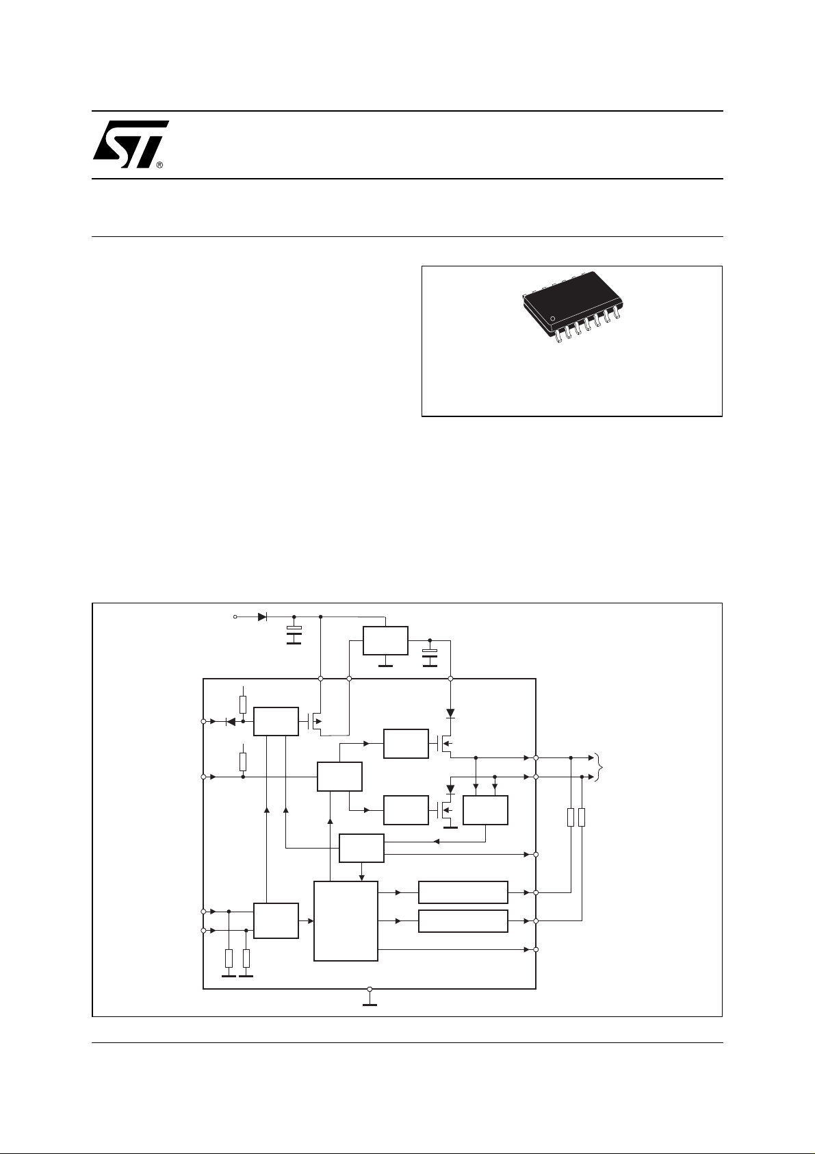
Figure 1. Block Diagram
KL30
(+12V)
5Vint
75k
7
WAKE
VCC
12.5k
2
TXD
5
NSTB
6
EN
99AT0001
Wake-up
Control
Low
Power
Control
100k100k
INHVS
14 1
TXD
Control
Receiver
Error
Management
& Diagnosis
Voltage
Regulator
13
GND
CANH
Driver
CANH
Driver
+5V
VCC
10
Filter
CANH T ermination
CANL T ermination
CANH
11
12
CANL
R
RTH
3
RXD
8
RTH
9
RTL
4
NERR
R
RTL
CAN
BUSLINE
July 2003
1/13
L9669
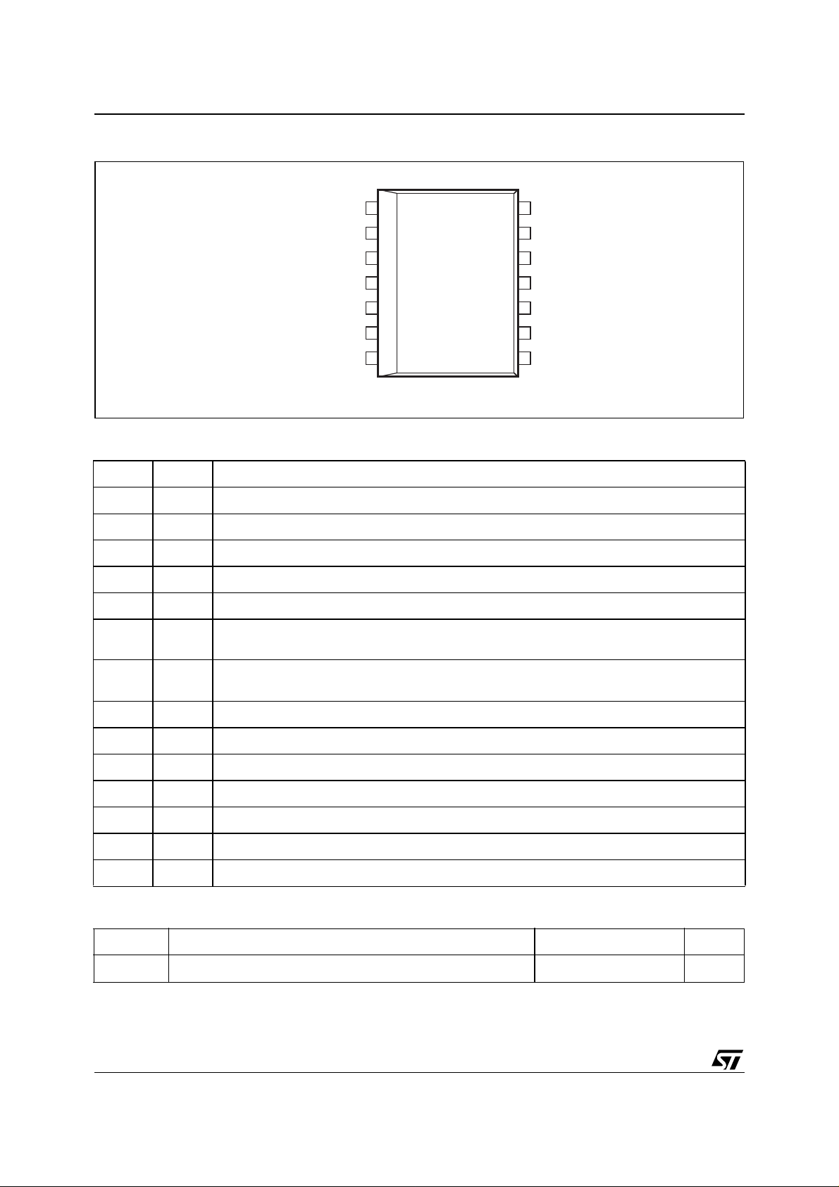
Figure 2. Pin Connection top view.
INH
TXD
RXD
NERR
NSTB
EN
WAKE
99AT0002
1
2
3
4
5
6
7
Table 1. Pin Functions
N° Pin Function
1INH
2TXD
3RXD
4NERR
5NSTB
Inhibit Output
Transmit Data Input
Receive Data Output
Error/Diagnostic Output
Not Standby Input
- for switching external 5V Regulator
- active LOW dominant Bit transmission
- active LOW dominant Bit reception
- Digital control signal for low power modes
- active LOW error/Wake-up and Diagnostic output
14
13
12
11
10
VS
GND
CANL
CANH
VCC
9
RTL
8
RTH
6EN
7 WAKE
8RTH
9RTL
10 VCC
11 CANH
12 CANL
13 GND Ground
14 VS
Enable Input/Diagnostic Clock
Digital control signal for low power modes/Diagnostic clock
Wake-Up Input
switching INH to VS
Termination Resistor for CANH
Termination Resistor for CANL
Supply Voltage Input
High Voltage Bus Line
Low Voltage Bus Line
Battery Voltage Input
- If level of V
- +5V
- High: dominant state
- Low: dominant state
- +12V
-
changes the device initiates a wake-up from sleep mode by
WAKE
- controlled by internal error management
- controlled by internal error management
Table 2. Thermal Data
Symbol Parameter Value Unit
R
thj-amb
Thermal resistance junction to ambient 120 °C/W
2/13
Table 3. Absolute Maximum Ratings
For externally applied voltages or currents exceeding these limits damage of the circuit may occur!
Symbol Parameter Value Unit
L9669
V
S-DC
V
S-P
V
CC
V
CANH,L-DC
V
V
WAKE
T
STG
T
Notes: 1. All pins of t he IC are pr otected aga inst ESD. T he verifica tion is perfor med accord ing to MIL 883C, hu man body mo del with
2. Voltage forced means voltage l i m i ted to spec i fied values while current is not l i m i ted. Current force d m eans voltage unlimi t ed but
DC operating battery voltage -0.3 to +28 V
Pulse operating battery voltage (t<400ms) -0.3 to +40 V
Supply voltage -0.3 to +6 V
DC voltage CANH, CANL -28 to +40 V
Voltage TXD, RXD, NERR, NSTB, EN -0.3 to VCC+0.3 V
X
Voltage WAKE -0.3 to VS+0.3 V
Storage temperature -55 to +150
Operating junction temperature -40 to +150
j
R = 1.5kΩ, C = 100pF and discharge vol t age ±2kV, corresponding to a m aximum discharge energy of 0.2mJ.
current li m i ted to specified value.
o
C
o
C
Table 4. Electrical Characteristcs
VCC= 4.75V to 5.25V, VS= 6V to 28V, Tj=-40°C to 150°C unless otherwise specified.
Item Symbol Parameter Test Condition Min. Typ. Max. Unit
1 Supplies
1.1 I
SSL
Supply current in sleep mode
= IVS)
(I
SSL
V
= 0V, VS = 14V 37 65 µA
CC
1.2 I
1.3 I
SSB
SND
Supply current in standby mode
= IVS + I
(I
SSB
Supply current in normal mode
(I
SND
2 CAN Line Interface
2.1 V
Differential receiver recessive to
r-d
dominant threshold
V
CANH
2.2 V
Differential receiver dominant to
d-r
recessive threshold
V
CANH
2.3 V
2.4 V
2.5 V
CANHr
CANHd
CANLr
CANH recessive output voltage V
CANH dominant output voltage V
CANL recessive output voltage V
= IVS + I
- V
CANL
- V
CANL
VCC
VCC
I
= 0 110 160 µA
INH
)
V
= 14V, V
)
S
(dominant state)
TXD
= 0
27 mA
no load at CAN
No bus errors.
= 5V
V
CC
No bus errors.
= 5V
V
CC
= V
TXD
RTH
TXD
TXD
RTH
CC
< 4kΩ
= 0V
= -40mA
= V
CC
< 4kΩ
R
I
CANH
R
-3.50 -2.20 V
-3.85 -2.5 V
0.35 V
VCC-
1.4
VCC-
0.2
V
V
3/13
L9669
Table 4. Electrical Characteristcs (continued)
VCC= 4.75V to 5.25V, VS= 6V to 28V, Tj=-40°C to 150°C unless otherwise specified.
Item Symbol Parameter Test Condition Min. Typ. Max. Unit
2.6 V
2.7 I
2.8 I
2.9 I
2.10 I
2.11
V
2.12
2.13 V
2.14 V
2.15
CANLd
CANH
CANL
CANHl
CANLl
CANHWK
V
CANLWK
CANHs
CANLs
V
CANHOV
CANL dominant output voltage V
CANH output current V
CANL output current V
CANH leakage current V
TXD
I
CANL
CANH
V
TXD
CANL
V
TXD
CANH
= 0V
= 40mA
= 0V
= 0V
= 5V
= 0V
= 14V
1.4 V
-160 -110 -70 mA
70 110 160 mA
0 µA
Sleep mode.
CANL leakage current V
CANL
= 0V
0 µA
Sleep mode.
CANH wake-up voltage Sleep/standby mode. 1.2 1.9 2.7 V
CANL wake-up voltage Sleep/standby mode. 2.4 3.1 3.8 V
CANH single ended receiver
threshold
CANL single ended receiver
threshold
CANH overvoltage detection
threshold
Normal mode.
= 5V
V
CC
Normal mode.
= 5V
V
CC
Normal mode.
= 5V
V
CC
1.5 1.8 2.15 V
2.7 3.1 3.4 V
7.2 V
2.16 V
CANLOV
2.17 t
2.18 t
2.19 t
2.20 t
2.21 t
wuCAN
2.22 t
drd
ddr
r,f
r,f
wuWK
CANL overvoltage detection
threshold
Propagation delay
TXD to RXD
recessive to dominant
Propagation delay
TXD to RXD
recessive to dominant
CANH, CANL output
rise/fall time
dominant to recessive
CANH, CANL output
rise/fall time
dominant to recessive
Minimum dominant time for
wake-up on CANH or CANL
Minimum pulse time for
wake-up on WAKE
Normal mode.
= 5V
V
CC
10% to 90%
= C2 = 3.3nF
C
1
7.2 V
1 1.6 µs
R1 = 100Ω
10% to 90%
= C2 = 3.3nF
C
1
2.2 µs
R1 = 100Ω
10% to 90%
= C2 = 3.3nF
C
1
0.6 1.5 µs
R1 = 100Ω
10% to 90%
= C2 = 3.3nF
C
1
2.6 6 µs
R1 = 100Ω
Sleep/standby mode. 8 44 µs
Sleep/standby mode 4 44 µs
4/13
 Loading...