

■
Modified VDMOS Power Stage (U
■
RDSON < 500 mOhm (Tj = 25°C)
■
CMOS Compatible Inputs
■
Enable Input (Reset)
■
Outputs Capable of up to 2.2 Amperes
■
Outputs Internally Clamped at 70V for Fast
DSBR
> 80V)
Inductive Load Switch Off
■
Wide operating supply voltage from 4.7V up to
30V
DIAGNO STIC FUNCTIONS
■
Open Load Detection (Output off, 100µsfiltering time)
■
Short to Ground Detection (Output off, 100µs filtering time)
■
Short to Battery Detection (Output on)
■
Over temperature detection (Output on)
■
Storage of last fault in 8 Bit - Serial Register
■
Fault Signal Indication at Serial Data Out
without need to read out the Serial Interface
■
Daisy Chainable Serial Diagnostic
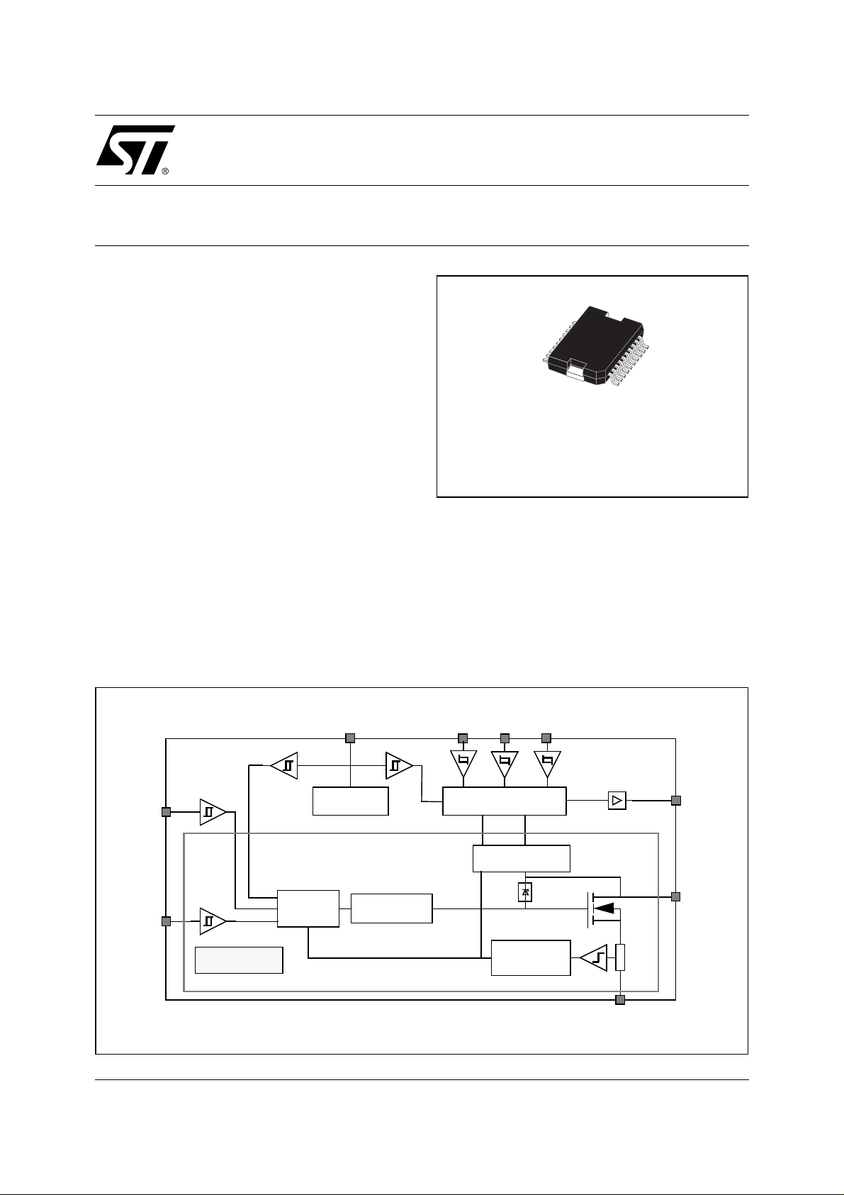
L9651
SMART QUAD SWITCH
PowerSO-20
ORDERING NUMBER: L9651
■
Serial Interface Clock Frequency up to 500kHz
DESCRIPTION
The L9651 consists of four identical low side power
switches. A serial diagnostic interface indicates failure mode of each switch (short circuit to V
ground and open load or over temperature).
BAT
or
BLOCK DIAGRAM
Reset
Inputs 1..4
April 2001
Four Fold
Turn On
Logic
V
BAT
Underv. Shutd.
●
References
Control
Gate
Data In
Clock Sync.
Serial Diagnostic
Fault Detection
Short Circuit
●
●
●
Protection
Serial Data Out
●
●
Output 1..4
Ground
1/9
L9651
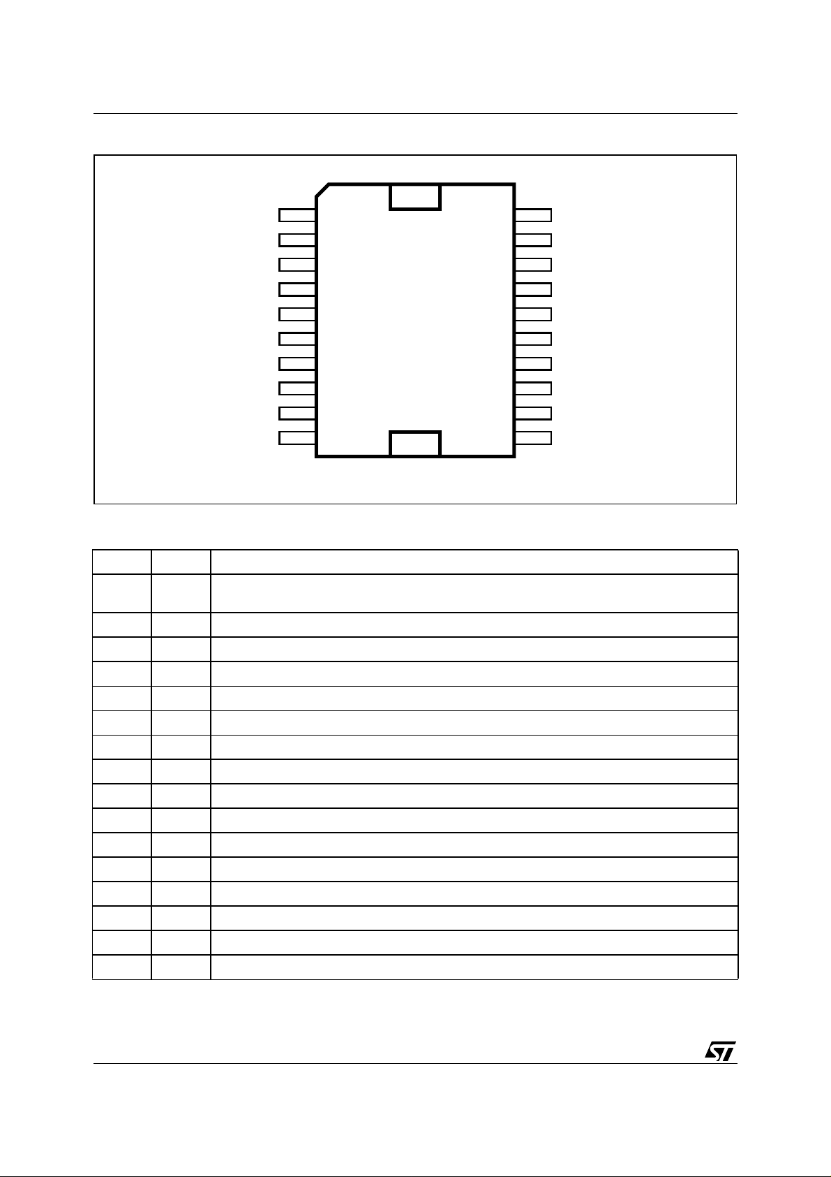
PIN CONNECTION
(Top view)
GND
N.C.
IN1
IN2
OUT1
VBAT
OUT2
DO
CL
1
2
3
4
5
6
7
8
9
GND 10
SO20POW
PIN FUNCTION
N° Pin Function
20
19
18
17
16
15
14
13
12
11
GND
N.C.
IN4
IN3
OUT4
R
OUT3
DI
SY
GND
1, 10,
11, 20
2, 19 N.C. Not Connected
3 IN1 Input 1
4 IN2 Input 2
5 OUT1 Output 1
6 VBAT Supply Voltage
7 OUT2 Output 2
8 DO Serial Data Out
9 CL Clock
12 SY Synchronization
13 DI Serial Data In
14 OUT3 Output 3
15 R Reset
16 OUT4 Output 4
17 IN3 Input 3
18 IN4 Input 4
GND Ground
2/9
ABSOLUTE MAXIMUM RATINGS
Symbol Parameter Value Unit
L9651
V
VR,V
VCLV
T
STG
T
V
BA T
V
BATtr
V
OUT
OUTtr
E
CL
-I
OUT
INi,VDI,
V
DO
Storage Temperature -55 to 150
Operating Junction Temperature -40 to 150
J
DC Supply Voltage -2 to 30 V
Transient Supply Voltage; t < 400ms 40 V
Output Voltage 65 V
Transient Output Voltage; during clamping 78 V
Output Clamping energy; repetition rate < 100 Hz 10 mJ
Output reverse current 2 A
Control Input voltage -0.3 to 6.5 V
SY
Control Output voltage -0.3 to 6.5 V
THERMAL DATA
Symbol Parameter Value Unit
R
th j-case
Thermal Resistance Junction to Case 2.5 °C/W
o
C
o
C
ELECTRICAL CHARACTERISTCS
(6.5V < V
< 25V, -40 < TJ < 150°C)
BAT
Symbol Parameter Test Condition Min. Typ. Max. Unit
Supply Voltage
V
BATU
I
BA T
Turn on threshold voltage 2.0 4.7 V
Supply current V
V
BAT
OUTi
= 14V
> 0V
41015mA
Output stage
R
DSON
V
On resistance V
Clamping voltage,
CL
= 14V
BAT
T
= 25°C; I
J
= 14V
V
BAT
T
= 150°C; I
J
I
= 0.5 A 63 70 76 V
out
out
= 1A
out
= 1A
500
850
inductive load
I
OUTi
Over current shutdown
= -40°C
T
J
3.0
4.3
(Shutdown latch resets
with pos. slope at INi)
= 25°C
T
J
= 150°C
T
J
2.5
2.2
3.7
3.5
Output leakage current see: Open load diagnostic current
mΩ
mΩ
A
A
A
3/9
 Loading...