

OPERATING POWER SUPPLY VOLTAGE
RANGE 4.5V ≤ V
≤ 36V (40V FOR TRAN-
S
SIENTS)
REVERSE SUPPLY (BATTERY) PRO-
TECTED DOWNTOV
≥ -24V
S
STANDBY MODE WITH VERY LOW CURRENT CONSUMPTIONIS
1µA@VCC0.5V
SB
LOW QUIESCENT CURRENT IN OFF CONDITIONIS
OFF
= 120µA
TTL COMPATIBLETX INPUT
BIDIRECTIONAL K-I/O PIN WITH SUPPLY
VOLTAGEDEPENDENT INPUTTHRESHOLD
OVERTEMPERATURE SHUT DOWN FUNC-
TION SELECTIVETO K-I/OPIN
WIDE INPUT AND OUTPUT VOLTAGE
RANGE-24V≤V
V
≤
K
S
K OUTPUT CURRENT LIMITATION, TYP IK=
60mA
DEFINEDOFF OUTPUT STATUS IN UNDERVOLTAGE CONDITION AND VS OR GND INTERRUPTION
CONTROLLED OUTPUT SLOPE FOR LOW
EMI
HIGH INPUT IMPEDANCE FOR OPEN V
OR
S
GND CONNECTION
L9637
ISO 9141 INTERFACE
SO8 Minidip
ORDERING NUMBERS:
L9637D L9637
DEFINED OUTPUT ON STATUS OF LO OR
RXFOROPENLIOR K INPUTS
DEFINED K OUTPUT OFF FOR TX INPUT
OPEN
INTEGRATED PULL UP RESISTORS FOR
TX, RX AND LO
EMI ROBUSTNESS OPTIMIZED
DESCRIPTION
The L9637 is a monolithic integrated circuit containing standard ISO 9141 compatible interface
functions.
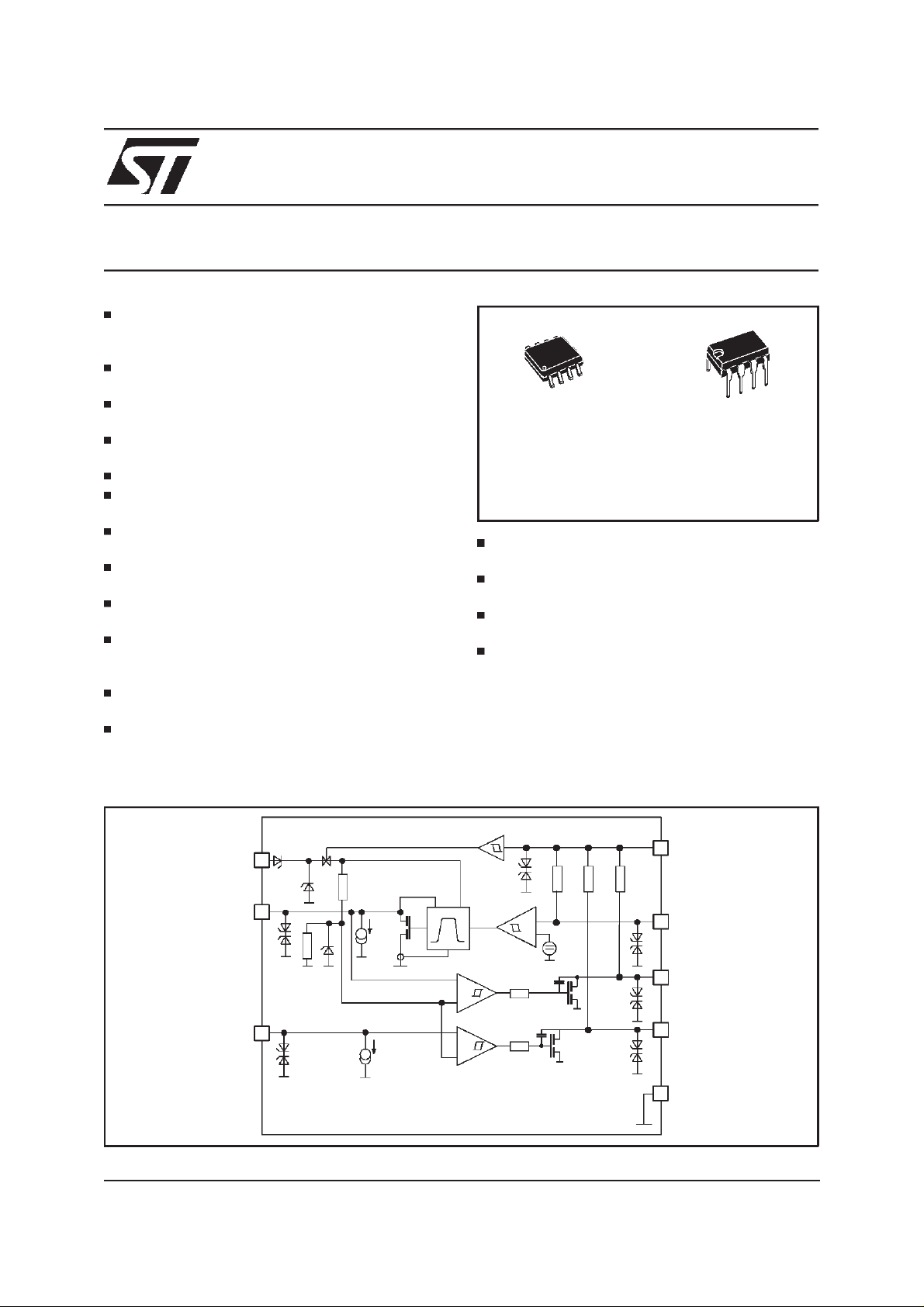
BLOCK DIAGRAM
December 1998
VS
RTX RLO RRX
K
IK
OFF
+
LI
ILI
+
-
+
1,75V
VCC
TX
RX
LO
GND
1/11
L9637
ABSOLUTE MAXIMUM RATINGS (Nodamage or latch)
Symbol Parameter Value Unit
V
S
Supply Voltage
ISO transients t = 400ms
V
CC
/dt Supply Voltage transient -10 to +10 V/µs
∆V
S
V
LI, K
V
LO, RX, TX
Note: Max. ESD voltages are ±2kV withhuman body model C= 100pF,R = 1.5k corresponds to maximumenergy dissipation0.2mJaccording
to MIL883C.
Stabilized Voltage -0.3 to +7 V
Pin Voltage -24 to V
Pin Voltage -24 to V
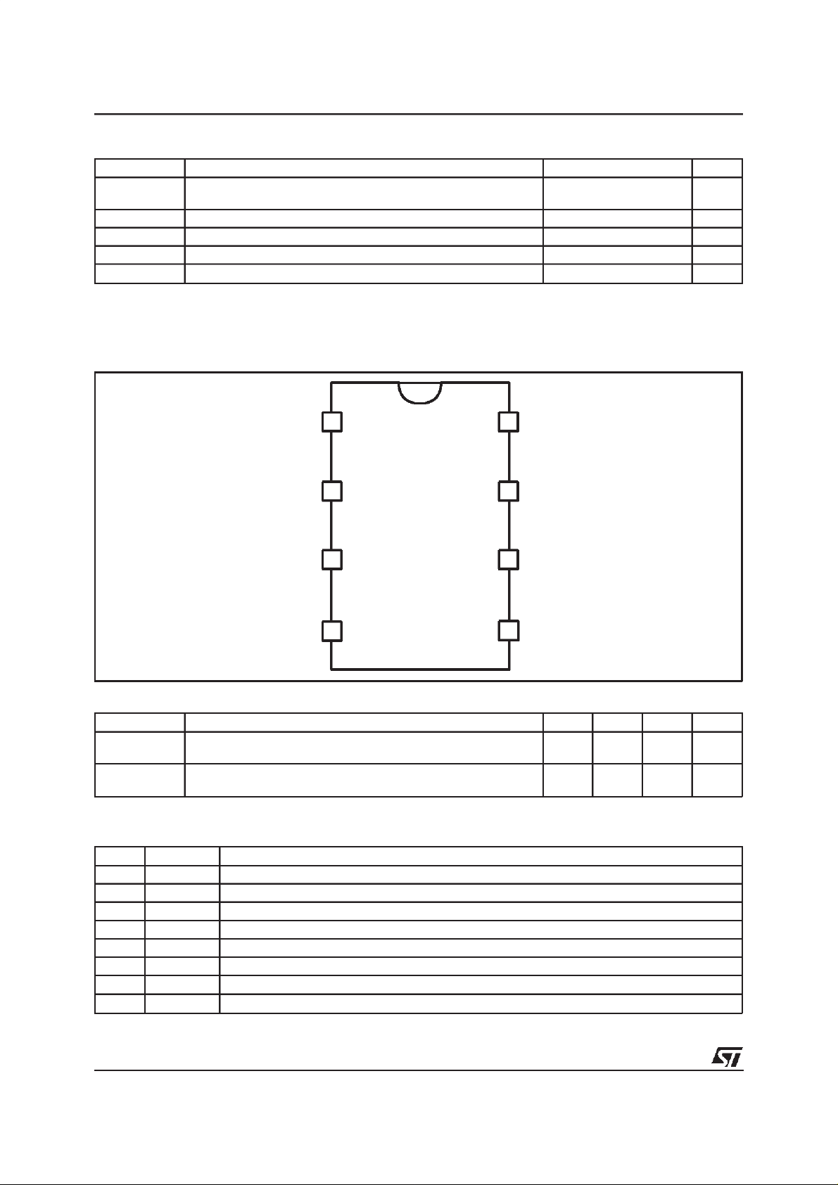
PIN CONNECTION(Top view)
RX
LO
1
2
8
LI
7
VS
-24 to +36
-24 to +40
CC
V
V
S
V
V
U537
VCC
TX
3
45
6
K
GND
THERMAL DATA
Symbol Parameter Min. Typ. Max. Unit
T
JSDon
T
JSDoff
R
th j-amb
Temperature K shutdown switch on threshold
Temperature K shutdown switch off threshold
Thermal steady state junction to ambient resistance for SO8
Thermal steady state junction to ambient resistance for Minidip
160
150
130
80
155
100
200
200
180
120
PIN DESCRIPTION
N. Name Function
1 RX Output for K as input
2 LO Output L comparator
3 VCC Stabilized voltage supply
4 TX Input for K as output
5 GND Common GND
6 K Bidirectional I/O
7 VS Supply voltage
8 LI Input L comparator
°C
C
°
C/W
°
°C/W
2/11
L9637
ELECTRICALCHARACTERISTICS (The electrical characteristicsare valid within the below defined op-
erating conditions, unless otherwise specified. The function is guaranteed by design until T
peratureshutdown switch-on-threshold.)
Symbol Parameter Test Condition Min. Typ. Max. Unit
V
S
V
CC
T
j
I
CC
IS
ON
IS
OFF
IS
SB
VK
low
VK
high
VK
hys
IK
off
RK
ON
IK
SC
VTX
VTX
RRX
RLO
IRX
ILO
VRX
VLO
RLO
RRX
RTX Input pull up resistance -0.15V≤VTX≤V
VLI
low
VL
high
VLI
hys
Supply Voltage 4.5 36 V
Stabilized Voltage 3 7 V
Junction temperature -40 150 °C
Supply VCCCurrent V
5.5V; VLI,VTX = 0V 1.4 2.3 mA
≤
CC
VK≥VK
; VLI≥VLI
high
high
-5 <1 5
VTX = VCC@VCC≤ 5.5V
Supply VS Current VS≤ 16V; VLI, VTX = 0V 1.2 3 mA
VK ≥ VK
VTX≥VTX
V
CC
Input Voltage Low state RX output status LOW
4.5V ≤ V
RX output status LOW
18V < V
Input Voltage High state RXoutput status HIGH
4.5V≤V
RX output status HIGH
18V < V
Input Threshold Hysteresis VK
high
Input Current @ VTX≥VTX
high
0.5V @ V
≤
S
S
S
S
-VK
; VLI ≥ VLI
high@VS
S
≤ 18V
18V
≤
low
high
high
12V
≤
12V <1
≤
-24 0.45V
-24 8 V
0.55V
S
12 V
-5 4 25
120 220 µA
0.025
V
S
VK ≤ VSVS,VCC≥ 0or
V
Output ON Impedance @ VS≥ 6.5V
VTX≤ VTX
S,VCC
low
= open
10 30 Ω
IK≥ 7mA 1)
Short Circuit Current 30 60 100 mA
Input voltage LOW state -24 1 V
low
Input voltage HIGH state 2.5 V
high
Output ON Impedance VK ≤ VK
ON
ON
Output Short Circuit Current 9 20 35 mA
SC
SC
Output Voltage HIGH state 10MΩ ≤ R
H
H
V
S
10MΩ ≤ R
6.5V I
≥
;VLI≤VLI
low
RX, LO
LRX
LLO
low
1mA 1) 40 90
≥
VCC-
0.25
VCC-
0.1
Output pull-up resistance Output status = (HIGH)
-0.15V ≤ VLO ≤ V
-0.15V ≤ VRX ≤ V
Input voltage LOW state LO output status LOW
4.5V ≤ V
≤ 18V
S
LO output status LOW 18V < V
Input voltage HIGH state LO output status HIGH
4.5V ≤ V
≤ 18V
S
LO outputstatusHIGH 18V < V
Input threshold hysteresis VLI
high
- VLI
low
+ 0.15V
CC
+ 0.15V
CC
+ 0.15V 10 20 40 K
CC
51020KΩ
-24 0.45V
-24 8 V
S
0.55V
S
12 VS V
S
0.025VS0.8 V
V
S
S
0.8 V
CC
V
CC
VS V
JSDon
S
S
tem-
A
µ
A
µ
V
V
V
A
µ
V
Ω
V
Ω
V
ILI Input current VLI ≤ V
SVS,VCC
V
S,VCC
≥ 0or
= open
-5 4 25 µA
3/11
L9637
ELECTRICALCHARACTERISTIC (continued)
Symbol Parameter Test Condition Min. Typ. Max. Unit
C
Ki, LO,RX
f
LI-LO
f
K-RX
f
TX-k
t
rLI-LO
t
rK-RX
t
rTX-K
t
fLI-LO
t
fK-RX
t
fTX-K
t
OFF,LI-LO
t
OFF,K-RX
t
OFF,TX-K
t
ON,LI-LO
t
ON,K-RX
t
ON,TX-K
1) For outputcurrents lower than this value a series protection diode can become active. See also Fig. 4 and 5.
Internal output capacities 20 pF
Transmission Frequency 9V < VS< 16V
(external loads)
R
= 510Ω,CK≤1.3nF
KO
50 100 kHz
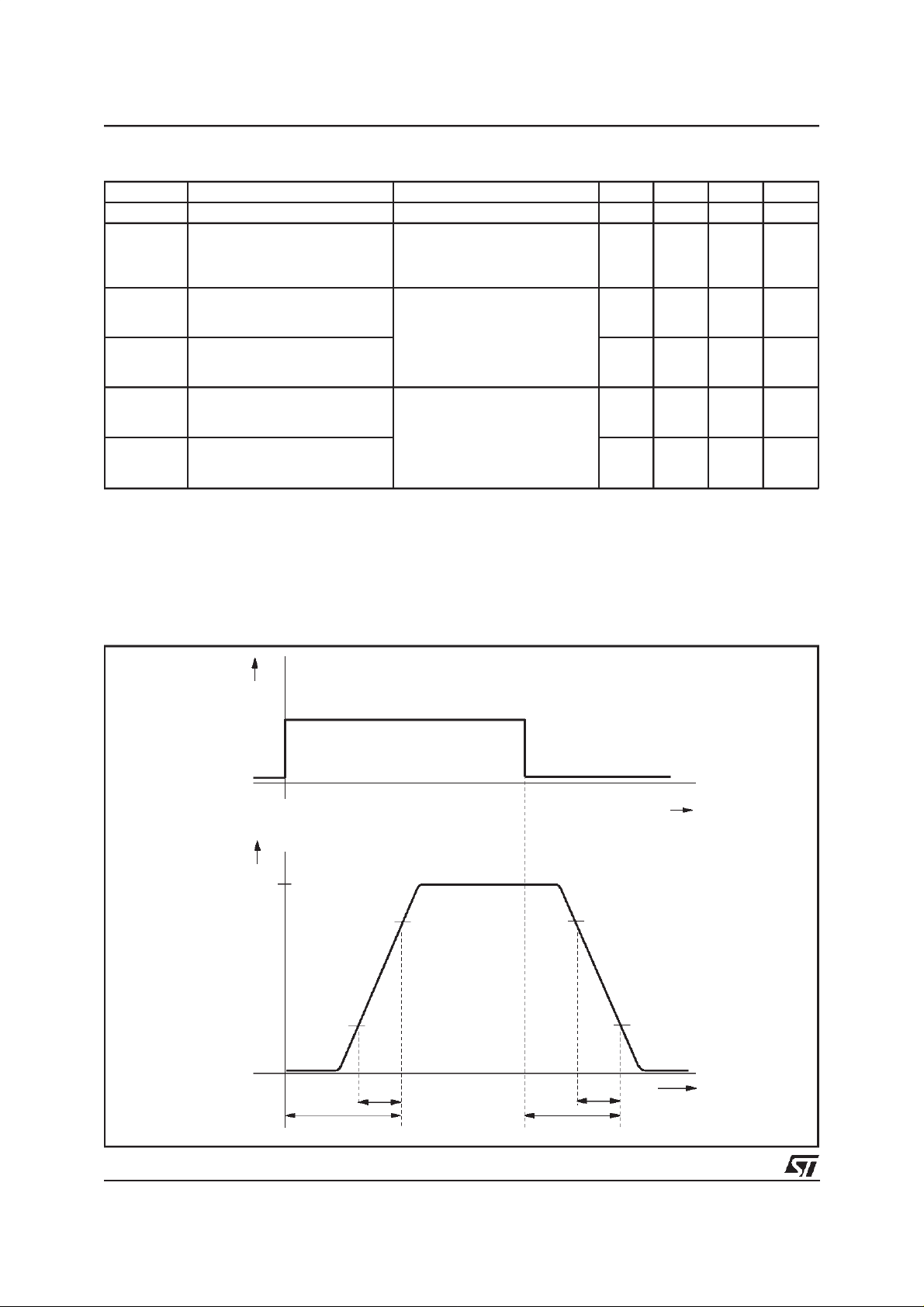
in active mode see Fig. 3
Rise Time for the definition of tr, tfsee
Fig.1.
Fall Time
9V < V
R
< 16V (external loads)
S
= 510Ω,CK≤1.3nF
KO
Switch OFF time for the definition of ton, t
Fig.1.
Switch ON time
9V < V
R
< 16V (external loads)
S
= 510Ω,CK≤1.3nF
KO
(inactive mode see Fig. 3)
OFF
see
26µs
26µs
417
417µs
s
µ
Figure 1:
Input to OutputTimings and Output Pulse Shape.
V
I
V
OUT
80% 80%
20%
t
20%
4/11
t
OFF
t
r
t
f
t
ON
t

Figure 2: ISOApplication Circuit
L9637
510 Ohm
0.4 Ohm
VS
Diagnostic
Tester
VS
40V
R
KO
K
K Line
C
K
LI
L Line
ECU1
K
C
K
IK
OFF
-
+
-
ILI
+
K
L
RTX RLO RRX
-
+
1,75V
VCC
TX
RX
LO
GND
I/O
I/O
I/O
5V
VCC
uP
VDD
LI
ECU2
FUNCTIONAL DESCRIPTION
The L9637 is a monolithic bus driver designed to
provide bidirectional serial communicationin automotive diagnostic applications according to the
specification”DiagnosticSystems ISO9141”.
The device provides a bidirectionallink, called K,
to the V
related diagnosis bus. It also includes
Bat
a separatecomparator L which is also able to be
linked to the V
RX of K are related to V
bus. The input TX and output
Bat
with her integrated pull
CC
up resistances. Also the L comparator output LO
has a pullup resistance connectedto V
CC
.
The maximum external pull up resistance at K related to V
should not be higher than RKO≤ 5KΩ
S
to achieve clear outputON conditions.
All V
bus defined inputs LI and K have supply
Bat
voltage dependent thresholds together with suf-
ficent hysteresis to suppress line spikes. These
pins are protected against overvoltages, shorts to
GND and V
and can also be driven beyond V
S
and GND. These features are also given for TX,
RX and LI only taking into account the behaviour
of the internal pull up resistances. The thermal
shut down function switches OFF the K output if
the chip temperatureincreases above the thermal
shut down threshold. To reactivate K again the
chip temperature must decrease below the K
switch ON temp.To achieve no fault forV
under-
S
voltage conditions the outputs will be switched
OFF and stay at high impedance. The device is
also protected against reverse battery condition.
During lack of V
or GND all pins shows high im-
S
pedance characteristic.To realize a lackof theV
related bus line LI and K the outputs LO and RX
showsdefined ON status.
S
S
5/11

L9637
Supressing all 4 classes of ”Schaffner”signals all
pins can be load with short energy pulses of max.
±0.2mJ. All these features together with a high
possible baud rate >50Kbaud, controlled output
slopes for low EMI, a wide power supply voltage
range and a very small quiescent current during
OFF (TX LI K=High) condition IS
off typ
≤ 120µA,
and a real standby function with zero power consumption IS
ing V
≤ 0.5V make this device high efficient for
CC
≤ 1µA during system depower-
SB typ
automotivebus system.
Figure 3: Typicaltimingfor modetransitions.
OFF active activeOFF
LI
After wake up of the system from OFF or SB
condition the first output signal will have an additional delay time td
≤ 5µs see also Fig. 3.
typ
The typical output voltage behaviour for the K,
LO, RX outputs as a functionof the output current
is shown in Fig.4. Fig.5 shows a waveform of the
output signal when the low level changes from
R
ON*IOUT
to I
*2*RON+UBEstate.Thisvari-
OUT
ation occurs due to too low output current or after
a negative transient forced to the output or to the
supplyvoltage line.
LO
TX
K
RX
6/11
tdt
ON
LI - LO
tdt
ON
TX - K

Figure 4: OutputCharacteristicsat K, LO, RX.
I
OUT
I
OUT
MIN
L9637
N
O
S
D
R
protection diode
Figure 5: OutputSignal Shape Related to OutputCurrent.
V
OUT
V
OUT
I
=
OUT DSON
I
=
OUT DSON
R
*
2
**
R
0.8V
+U
BE
V
OUT
I
OUT DS ON
R
2
**
I
OUT DSON
V
IN
t
V
OUT
+U
BE
R
*
t
I
OUT
I
I
>
OUT
OUT
>
I
OUT
MIN
I
OUT
I
<
OUT
MIN
MIN
7/11

L9637
Figure 6: EMSPerformance(ISO 9141 BUS system).
VS = 12V
=
510 Ohm
10kHz
D
Signal comparison
∆≤± 10%
D£ 10 %
Figure 7.
P
i(mW )
10000
50 Ohm
VS
TX K
IS O i n te rface
VS
RX
IS O i n te rface
1.5nF
K
not incident power resistant
136 Ohm
68 Ohm
Probe
NAP - 73
P
i
NAP
P
ima x
40dB
=5W
Rhode
& Schwartz
SMG
0.1 - 1000MH z
8/11
5000
1000
incident power resistant
100
1 10 100 1000
f
(M H z)

L9637
DIM.
MIN. TYP. MAX. MIN. TYP. MAX.
A 1.75 0.069
a1 0.1 0.25 0.004 0.010
a2 1.65
a3 0.65 0.85 0.026 0.033
b 0.35 0.48 0.014 0.019
b1 0.19 0.25 0.007 0.010
C 0.25 0.5 0.010 0.020
c1 45° (typ.)
D (1) 4.8 5.0 0.189 0.197
E 5.8 6.2 0.228 0.244
e 1.27 0.050
e3 3.81 0.150
F (1) 3.8 4.0 0.15 0.157
L 0.4 1.27 0.016 0.050
M 0.6 0.024
S8°(max.)
mm inch
0.065
OUTLINE AND
MECHANICAL DATA
SO8
(1) D and F do not include moldflash or protrusions. Moldflash or
potrusions shallnot exceed 0.15mm (.006inch).
9/11

L9637
DIM.
MIN. TYP. MAX. MIN. TYP. MAX.
A 3.32 0.131
a1 0.51 0.020
B 1.15 1.65 0.045 0.065
b 0.356 0.55 0.014 0.022
b1 0.204 0.304 0.008 0.012
D 10.92 0.430
E 7.95 9.75 0.313 0.384
e 2.54 0.100
e3 7.62 0.300
e4 7.62 0.300
F 6.6 0.260
I 5.08 0.200
L 3.18 3.81 0.125 0.150
Z 1.52 0.060
mm inch
OUTLINE AND
MECHANICAL DATA
Minidip
10/11

L9637
Information furnished is believed to be accurate and reliable. However, STMicroelectronics assumes no responsibility for the consequences
of use of such information nor for any infringement of patents or other rights of third parties which may result from its use. No license is
granted by implication or otherwise under any patent or patent rights of STMicroelectronics. Specification mentioned in this publication are
subject to change without notice. This publication supersedes and replaces all information previously supplied. STMicroelectronics products
are not authorized for use as critical components in life support devices or systems without express written approval of STMicroelectronics.
The ST logo is a registered trademark of STMicroelectronics
1998 STMicroelectronics – Printed in Italy – AllRights Reserved
STMicroelectronics GROUP OF COMPANIES
Australia - Brazil - Canada - China - France - Germany - Italy - Japan - Korea - Malaysia - Malta - Mexico - Morocco - The Netherlands -
Singapore - Spain - Sweden - Switzerland - Taiwan - Thailand - United Kingdom - U.S.A.
http://www.st.com
11/11
 Loading...