

PWMPOWER MOS CONTROLLER
.HIGH EFFICIENCY DUE TO PWM CONTROL
ANDPOWERMOSDRIVER
.LOADDUMP PROTECTION
.LOADPOWERLIMITATION
.EXTERNALPOWERMOSPROTECTION
.LIMITEDOUTPUTVOLTAGESLEWRATE
DESCRIPTION
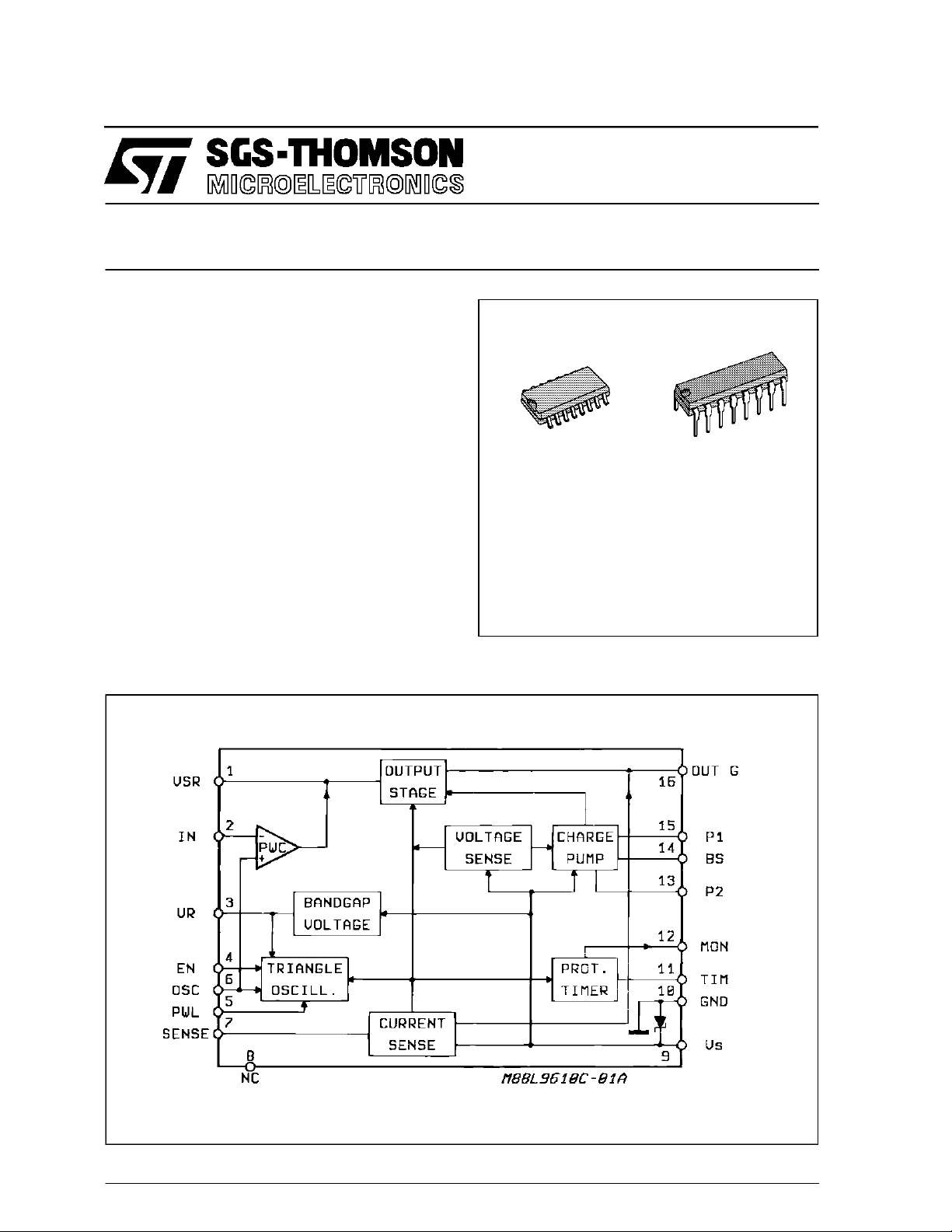
The L9610C/11Cis a monolithic integrated circuit
workingin PWM mode as controller of an external
powerMOStransistorinHighSide Driver configuration.
Features of the device include controlled slope of
the leadingand trailing edgeof the gate drivingvoltage,linearcurrentlimitingwithprotectiontimer,settableswitchingfrequencyfo,TTLcompatibleenable
function,protectionstatus ouput pin. Thedevice is
mountedin SO16micropackage,and DIP16package.
L9610C
L9611C
SO16
ORDERING NUMBERS: L9610C
DIP16
L9611C
BLOCK DIAGRAM
November 1991
This is advanced informationon a new product now in development or undergoing evaluation. Details are subject to change withoutnotice.
1/9
L9610C - L9611C
ABSOLUTE MAXIMUM RATINGS
Symbol Parameter Value Unit
V
Max. Supply Voltage 26 V
S
Transient Peak Supply Voltage (R1 ≥ 100Ω):
Load Dump:
5ms ≤ t
≤ 10ms; τfFall Time Constant = 100ms; R
rise
SOURCE
≥ 0.5Ω
60
Field Decay:
5ms ≤ t
≤ 10ms; τrRise Time Constant = 33ms; R
fall
SOURCE
≥ 10Ω
–80
V
V
T
J/Tstg
Low Energy Spike: t
I
V
Max. Supply Current (t < 300 ms) 0.3 A
S
Input Voltage –0.3 < VIN<VS– 2.5 V
IN
rise
=1µs, t
Junction and Storage Temperature Range – 55 to 150 °C
= 2ms, R
fall
SOURCE
≥ 10Ω
±100
THERMAL DATA
Symbol Parameter SO16 DIP16 Value
R
th j-amb
Thermal Resistance Junction-alumina Max 50 90 °C/W
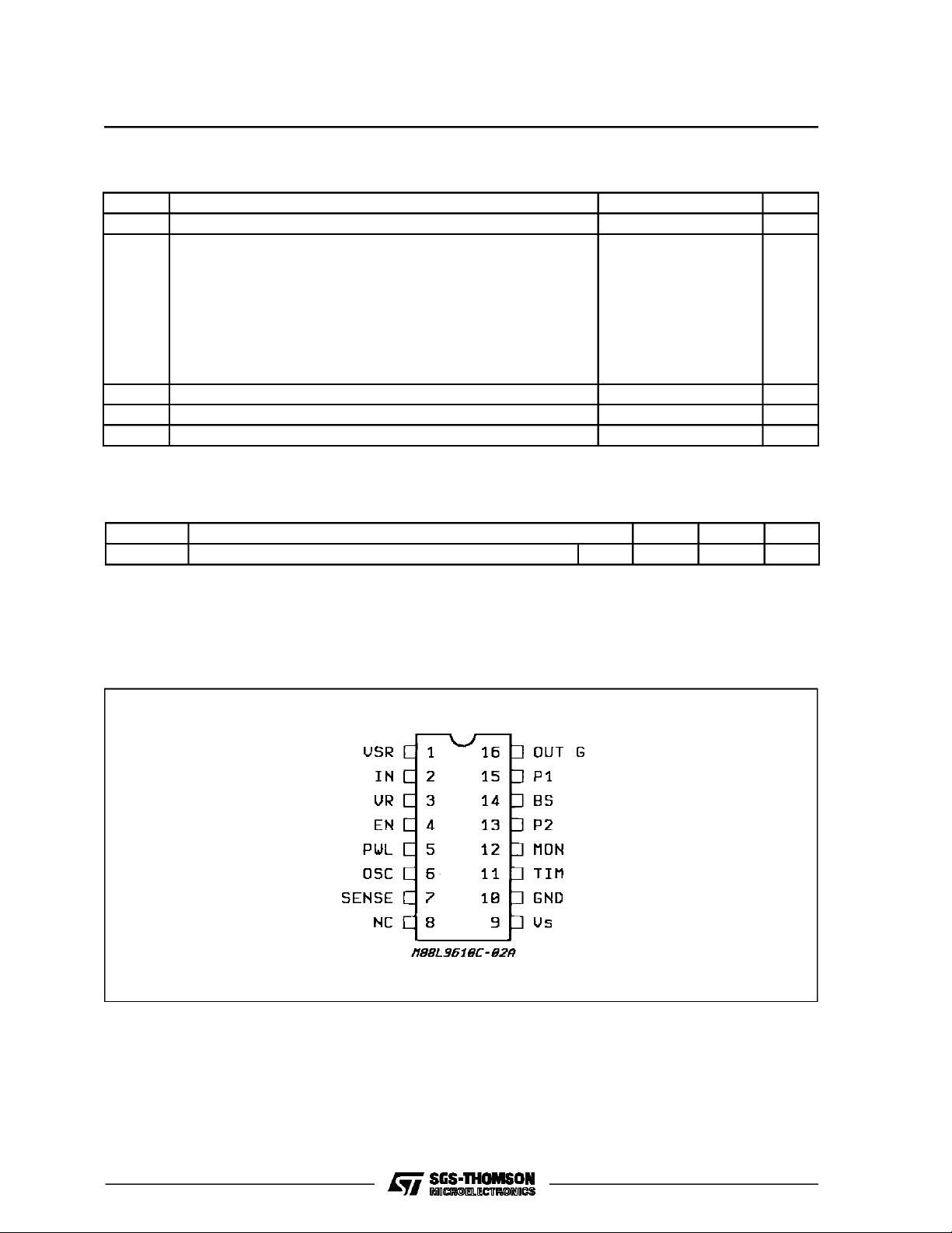
PI N CONNECTI O N (Top view)
V
2/12

L9610C - L9611C
PIN FUNCTIONS
Pin Name Functions
1 INT A Capacitor Connected Between this Pin and Out
Voltage Slew Rate.
2 IN Analog Input Controlling the PWM Ratio. The operating range of the input
.
R
3V
R
voltage is 0 to V
Output of an Internal Voltage Reference
4 EN TTL Compatible Input for Switching off the Output.
5 PWL If this Pin is Connected to GND and V
Frequency f
are Reduced : this Allows to Transfera Costant Power to the
o
> 13 V, the Duty Cycle and the
S
Load.
6 Osc Current Sink and Source StageConnection of a Triangle Oscillator with
Definite Voltage Swing.
7 IND Input of an Operational Amplifier for Short Current Sensing and Regulation.
8 NC Not Connected.
9V
S
Common Supply Voltage Input
10 GND Common Ground Connection
11 TIM A Capacitor Connected Between this Pin and GND Defines the Protection
Delay Time.
12 MON Open Collector Monitoring Output off the PowerMOS Protection.
13,15 P2, P1 Connection for the Charge Pump Capacitor.
14 BS The Capacitor Connected Between thisPin and theSource of the Power MOS
Allows to Bootstrap the Gate Driving Voltage.
16 Out G Output for Driving the Gate of the External PowerMOS.
Defines the GATE
G
3/12
L9610C - L9611C
ELECTRICAL CHARACTERISITCS (T
=–40°Cto85°C;6V<VS<16 V unless otherwise specified)
amb
Symbol Parameter Test Conditions Min. Typ. Max. Unit
V
S
I
q
V
SC
V
SH
V
SL
V
R
I
R
V
INL
K
F
K
S
Operating Supply Voltage 6 16 V
Quiescent Current 2.5 6 mA
Internal Supply Voltage Clamp IS= 200mA 28 32 36 V
Supply Voltage High Threshold 16 18.5 21 V
Supply Voltage Low Threshold 4 5 6 V
Reference Voltage 3.3 3.5 3.7 V
Reference Current ∆VR≤ 100mV 1 mA
Input Low Threshold 0.13 0.15 0.2 VIN/V
Oscillator Freq. Constant Note 1 800 2500 nF/s
Gate Voltage Slew Rate
Note 2 3 5 9 nFV/ms
Constant
Protection Time Delay Constant Note 3 0.12 0.44 ms/nF
Sense Input Volt. 80 100 120 mV
Gate Driving Volt. above V
VS= 16V 8 16 V
S
Gate Voltage in OFF Condition IG= 100 µA 1.2 V
Input Current – 5 – 1 µA
Low Enable Voltage 0.8 V
High Enable Voltage 2.0 V
V
V
V
V
K
T
V
Si
GON
GOFF
I
IN
ENL
ENH
IEN Enable Input Current 2 µA
SR Slew Rate Without C
V
MONsat
Saturation Voltage (pin 12) I
MON = 2.5 mA
S
0.5 V/µs
1.5 V
R
Notes : 1. fo=KF/CF.
2. dV
3. t
prot=KTCT
/dt= Ks/Cs.
G
.
FUNCTIONAL DE SCRI PTION
PULSEWIDTH COMPARATOR
A ground compatible comparator generates the
PWMsignal whichcontrols thegate of theexternal
powerMOS.
Theslopes of the leadingand trailing edges of the
gate driving signal are defined by the external capacitorC
accordingto :
S
dV
/dt= KS/C
G
S
Thisfeature allowsto optimize theswitching speed
for the powerand RFIperformancebest suitedfor
the application.
Thelowerlimit of theduty cycle is fixedat 15% of
the ratio between the input and the reference voltage(seefig.1).Inputvoltageslowerthanthisvalue
disable the internal oscillator signal and therefore
the gate driver.
GROUNDCOMPATIBLETRIANGLE
OSCILLATOR
The triangle oscillator provides the switching frequencyf
setbytheexternalcapacitorCFaccording
o
to :
f
o=KF/CF
If the pin PWL (power limitation) is connected to
ground and Vs is higher than the PWL threshold
voltage,the duty cycle and thef
frequencyare re-
o
duced:this allowstotransferacostantpowertothe
load (seefig.2).
TIMERAND PROTECTIONLATCH
When an overcurrent occurs, the device starts
chargingthe externalcapacitorC
; the protection
T
time is set accordingto :
.
t
prot=KT
C
T
4/12

L9610C - L9611C
Afterthe overcurrentprotectiontimeis reached,the
powerMOSisswitched-off; thisconditionis latched
by settinganinternalflip-flopandis externallymonitored by the low state of theMON pin.
Toresetthelatchthesupplyvoltagehastofallbelow
or the devicemust beswitchedoff.
V
SL
UNDER AND OVERVOLTAGE SENSE WITH
LOADDUMP PROTECTION
The undervoltagedetectionfeatureresetsthetimer
and switchesoff theoutputdrivingsignal when the
supplyvoltageisless than V
SL
.
If the supply voltage exceeds the max operating
supply voltage value, an internal comparator disablesthe chargepump,theoscillatorandtheexternal powerMOS.
Figure1 : TypicalTransferCurve.
In both casesthe thresholdsare providedwith suitable hysteresisvalues.
Theloaddumpprotectionfunctionallowsthedevice
to withstand- for alimited time - highovervoltages.
It consistsof an active clamping diodewhich limits
the circuitsupplyvoltageto V
andanexternal
CLAMP
current limiting resistor R1. The maximum pulse
supply current (see abs. max. ratings is equal to
0.3A.Thereforethemaximum loaddumpvoltageis
givenby :
V
DUMP=VSC
+0.3R
1
In this conditionthe gate of the powerMOSis held
at the GNDpin potentialand thusthe loadvoltage
is :
V
=Vs-V
L
CLAMP-VGS
5/12

L9610C - L9611C
Figure2 : The Typical Waveformsfor the PowerLimitationFunction.
SHORTCIRCUITCURRENT REGULATION
The maximum load currentin the short circuitcon-
dition can be chosen by the value of the current
sensingresistorR
I
SC=VSI/RS
accordingto :
S
Two identicalVScompatiblecomparators are provided to realize the short circuit protection.
After reaching the lower thresholdvoltage (typical
value V
-10 mV), the first comparator enablesthe
SI
timer and the gateis drivenwith the fullcontinuous
pump voltage : when the upper threshold voltage
valueis reachedthe secondcomparatormaintains
the chosenI
drivingtheNMOSgatein continuous
SC
mode.
This function - showed in fig. 3 - speeds up the
switchon phase fora lamp as a load.
BANDGAP VOLTAGEREFERENCE
The circuitprovidesa referencevoltagewhichmay
6/12
beusedas controlinputvoltagethrougha resistive
divider.Thisreferenceisprotectedagainsttheshort
circuitcurrent.
CHARGEPUMP
The charge pump circuit holds the N-MOS gate
abovethesupplyvoltageduringtheONphase.This
circuitconsistsofanRCastablewhichdrivesacomparatorwith a push-pulloutputstage. The external
chargepumpcapacitorC
mustbeat least equalto
P
the NMOSparasiticinput capacitance.
ForfastgatevoltagevariationC
mustbeincreased
P
orthebootstrapfunctioncanbeused.Thebootstrap
capacitorshould be at least 10 times greater than
the powerMOSparasiticcapacitance.
The chargepump voltageV
V
=2VS-VBE-V
PUMP
canreach to :
PUMP
CESAT
Thecircuitis disabledifthe supplyvoltageis higher
SH
.
thanV

Figure3 : The Typical Waveformsfor ShortCircuit Current Condition.
L9610C - L9611C
7/12

L9610C - L9611C
APP LI CATI O N CI RCUI T
Figure4.
Note : Allnode voltages arereferred to groundpin (GND)
The currents flowing in the arrow direction are assumed positive
without C
without C
= 1nF
BS:CP
mustbe at least 10 times higher than the gate capacitance : CP= 100 pF.
BS:CBS
CONTROLLINGA 120W HALOGEN LAMP WITH
THEL9610C/11CDIMMER
The L9610C/11CLamp Dimmer is used to control
the brightnessof vehicleheadlampsusingH4 type
lamps(see fig. 5). With switchS1openthe fullsupply voltage is applied to the lamps : closing the
8/12
switch it is a possible to reduce the averagelamp
voltageas desired:
R3
VL = VS
R2+ R3
If pin 5 is connected to ground the average lamp
voltageis constant,even forsupply voltagesin excessof 13V.

Figure5 : ApplicationCircuit.
L9610C - L9611C
The sensing resistor R
and timing capacitor C
S
shouldbe dimensionedaccordingto :
V
RS=
2Inom (@Vs=14V)
2 xlimitation time
C
=
t
Si
K
T
In normal conditions(VCC=14V, maximum brightness) the voltage drop across the sense resistor
must be 50 mV. The current limiter intervenes
attwicethe nominalcurrent,I
nom
.
ThetimingcapacitorC
t
=3.5V)mustbechosen
t(Vct
sothatthedelay beforeinterventionistwicethe durationof the current limitationat power-on.
Theoptimalvalueofthe oscillatorfrequency,taking
tolerancesintoaccount,mustbeslightlyhigherthan
the frequencyat whichlampflicker isnoticable(min
60Hz).
The switching times are a compromise between
possibleEMI andswitchingpower losses.The recommendedvaluefor Cs is47pF.
9/12

L9610C - L9611C
DIP16 PACKAGE MECHANICAL DATA
DIM.
MIN. TYP. MAX. MIN. TYP. MAX.
a1 0.51 0.020
B 0.77 1.65 0.030 0.065
b 0.5 0.020
b1 0.25 0.010
D 20 0.787
E 8.5 0.335
e 2.54 0.100
e3 17.78 0.700
F 7.1 0.280
I 5.1 0.201
L 3.3 0.130
Z 1.27 0.050
mm inch
10/12

L9610C - L9611C
DIM.
MIN. TYP. MAX. MIN. TYP. MAX.
A 1.75 0.069
a1 0.1 0.25 0.004 0.009
a2 1.6 0.063
b 0.35 0.46 0.014 0.018
b1 0.19 0.25 0.007 0.010
C 0.5 0.020
c1 45 (typ.)
D 9.8 10 0.386 0.394
E 5.8 6.2 0.228 0.244
e 1.27 0.050
e3 8.89 0.350
F 3.8 4.0 0.150 0.157
L 0.4 1.27 0.016 0.050
M 0.62 0.024
S 8 (max.)
mm inch
11/12

L9610C - L9611C
Information furnished is believed to be accurate and reliable. However, SGS-THOMSON Microelectronics assumes no responsibility for
the consequences of use of such information nor for any infringement of patents or other rights of third parties which may result from its
use. No license is granted by implication or otherwise under any patent or patent rights of SGS-THOMSON Microelectronics. Specifications mentioned in this publication are subject to change without notice. This publication supersedes and replaces all information previously supplied. SGS-THOMSON Microelectronics products are not authorized for use as critical components in life support devices or
systems without express written approval of SGS-THOMSON Microelectronics.
1994 SGS-THOMSON Microelectronics- All Rights Reserved
Australia - Brazil - France - Germany - Hong Kong - Italy - Japan - Korea - Malaysia - Malta - Morocco - The Netherlands - Singapore-
SGS-THOMSON Microelectronics GROUP OF COMPANIES
Spain - Sweden- Switzerland - Taiwan - Thaliand- United Kingdom - U.S.A.
12/12
 Loading...