

CAR ALTERNATOR VOLTAGE REGULATOR
■ FULLY MONOLI THIC D ESIGN
■ LOW SIDE FIELD DRIVER
■ THERMAL PROTECTION
■ FIELD SHORT CIRCUIT PROTECTION
■ PROTECTED DIAGNOSTIC LAMP DRIVER
■ PROTECTED HIGH SIDE RELAY DRIVER
■ COMPLEX DIAGNO STICS
■ LOAD RESPONSE CONTROL
■ DFM OUTPUT (FIELD MONITOR)
DESCRIPTION
The L9407F is a monolithic multifunction alternator
voltage regulator intended for use in automotive application. It inc ludes the control s ection, the field power stage, fault diagnostic circuit which drives a
warning lamp, and the protection against short circuits .
CIRCUIT OPERATION
The alternator's voltage regulator performs the following main functions:
– 1) voltage regulation
– 2) protection
– 3) control fault diagnosis
– 4) load response control
L9407F
PRODUCT PREVIEW
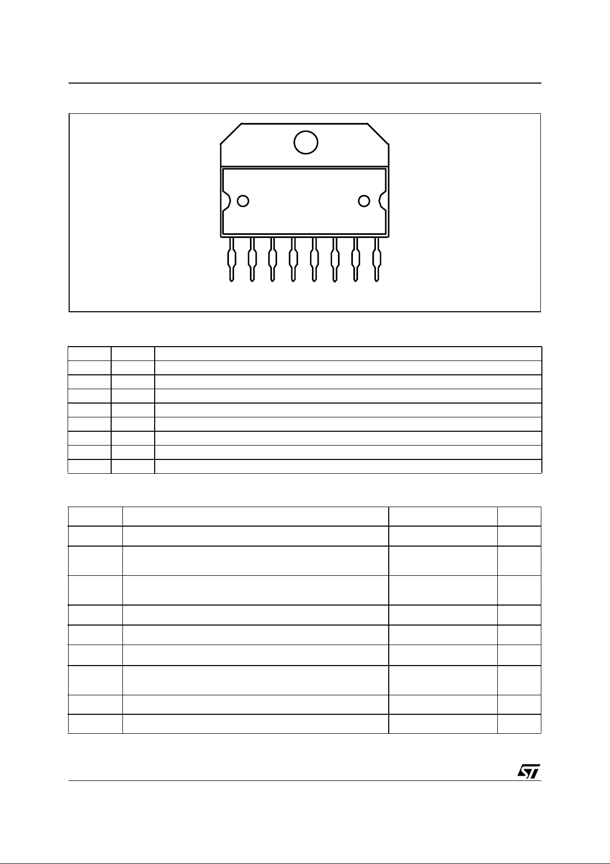
Multiwatt 8
ORDERING NUMBER: L9407F
device also with very long cables connecting the alternator to the battery with an impedance so high to
cause a superimposed ripple on the alternator voltage higher than 5-6V. Consequently it doesn't need,
in the standard application, any external component.
Anyway an external application (2.2uF or 2.7uF)
must be inserted be tween A+ and gr ound when using
the device with very long cables.
PROTECTION
It is present a protection against short circuits of the
lamp and the relay power drivers (D+) and of the field
power driver (DF), a thermal drivers shutdown protection and an overvoltage protection of D+ power
drivers.
VOLTAGE REGULATION
The alternator voltage is compared with a reference
voltage in an amplifier, whose output determines the
switching frequency of output power MOS whose
current excites the coil of the alternator; as the regulators are a self-oscillating type this frequency depends on the whole system parameter set including
DIAGNOSIS
The circuit detects fault conditions related to the
phase and DF status and receives informations from
one of the three alternator phas es. In order to prevent
spurious indications, fault warnings are not displa yed
immediately but are dalayed by a fixed time.
the alternator characteristics. The regulators have an
integrated filter in the voltage sensing path guaranteeing the correct behavio ur of the devices also when
the rectifier diodes feature very high switching
spikes. The internal filtering allows the usage of the
February 2003
This is preliminary information on a new product now in development. Details are subject to change without notice.
LOAD RESPONSE CONTROL
The internal circuit regulates the soft start characteristics (activated always at engine start) and the soft
attack characteristics.
1/11
L9407F
PIN CONNECTION
12345678
D+
A+
NC
DF
GND
DFM
NC
PH
PIN DESCRIPTION
N° Pin Function
1 D+ Lamp terminal low side driver; relay terminal high side driver
2 A+ Alternator output voltage supply
3 NC Not connected
4 DF Field low side driver output
5 GND Ground
6 DFM Field monitor output
7 NC Not connected
8 PH Phase sense input
ABSOLUTE MAXIMUM RATINGS
Symbol Parameter Value Unit
V
DC Supply Voltage (2 min. @ 25°C) [all pins vs. GND] 24 V
S
Transient Supply Voltage (load dump) [see application circuit]
t<500ms
Transient Supply Voltage (low energy spikes) [see application
circuit] ISO7637-1 pulse 1,2,3 /ISO7637-3
100 (clamped at 60 by
40 V
application)
V
T
2/11
stg
P
T
, T
tot
Junction temperature range -40 to 170 °C
j
Storage and case temperature range -40 to 150 °C
case
Total
power Dissipation (@ Tcase = 150°C, Ifield = 5A)
Reverse Voltage (see application diagram) @ 25°C, T = 15 sec
all pins, except for PH (normal working condition)
DC Pin Current on DF, A+, GND (bonding limitation) 15 A
ESD Voltage MILSTD883C (All pins vs.GND) ±4 KV
8W
-2.5 V
THERMAL DATA
Symbol Parameter Value Unit
L9407F
R
th j-case
ELECTRICAL CHARACTERISTCS
(T
= -40ºC ÷ 150ºC; unless otherwise specified)
case
Symbol Parameter Test Condition Min. Typ. Max Unit
Vbat Operating Supply Voltage 6 18 V
Ib-sinked Supply Battery Current 50 mA
Ib-stby Stand-by Current Vbat = A+, DF = 12.5V 500 uA
Vreg Regulated Volt. & Therm. Drift
fsw Switching Frequency preexcitation 30 400 Hz
Vreg Reg. Voltage without Battery Ialt = 3A resistive; Tcase=25º;
Thermal Resistance Junction to Case 0.6 °C/W
Ialt=1A-0.9*Inom; Tcase=20ºC;
1200<rpm<RPMMAX;
Vreg clamped at 14.8V Max. (Fig.3)
Delta Vrpm 1500<rpm<RPMMAX; Ialt=5A;
Tcase=23ºC
Delta Vload 5A<Ialt<Inom; rpm=6000rpm;
Tcase=23ºC
2000<rpm<RPMMAX
13.9
-4.5
14.35
-3.5
12 16 V
14.8
-2.5VmV/°C
200 mV
250 mV
Vov D+ Drivers Disable Threshold Voltage on pin A+ to have D+
Tj-sd Thermal Shut-down D+/DF = OFF STATE 180 200 220 ºC
Tj-sd-hys Thermal Shut-down hysteresis D+/DF from OFF STATE (due to
Vuv Low voltage detection
threshold
Vuv-hys Low voltage detection
threshold hysteresis
Ron LSD Low Side Driver Rdson T = 150ºC; I = 4.5A 189 mΩ
Ron LSD Low Side Driver Rdson T = 25ºC; I = 7A 107 mOhm
Vf Freewheeling diode DF I=5A 2 V
If_SCTH Short Circuit Threshold DF DF = 12V; Tcase = -40ºC 11 18 A
Vs1 Output Short to GROUND DF
Threshold
FS_duty Pre-excitation F.S.D.F. f = 333Hz +/- 15% 15.93 18.75 21.57 %
OFF
thermal shutdown) to ON STATE
D+ low side driver ON after
diagnosis delay time
D+ low side driver OFF without
delay
DF = 12V; Tcase = -25ºC 8.5 18 A
DF = 12V; Tcase = -150ºC 5.5 18 A
2.1 3.9 V
18 22 V
Tj-sd-2 Tj-sd-10 ºC
7.7 8.6 9.5 V
Vuv +
0.40
Vuv +
0.50
Vuv +
0.60
V
3/11
L9407F
ELECTRICAL CHARACTERISTCS
(T
= -40ºC ÷ 150ºC; unless otherwise specified)
case
Symbol Parameter Test Condition Min. Typ. Max Unit
t_ST Soft Start Delay Time (see fig. 5)activated always at engine start 0 s
t_SL Soft Attack Time / Soft Start
Time (see fig. 5)
Bl Soft Attack Blind Zone percentage of maximum duty
t-rise Output Voltage Rise Time Ifield = 3A resistive (Fig. 6) 4 50 µs
t_fall Output Voltage Fall Time Ifield = 3A resistive (Fig. 6) 5 50 µs
If_leak Output Field Driver Leakage
Current
VH_SAT High Side Driver Saturation
VL_SAT1 Low Side Driver Saturation
VL_SAT2 Low Side Driver Saturation
Voltage (Fig. 9)
Voltage
Voltage
(continued)
from 0 to 100% field duty cycle 2.45 3 3.45 s
010%
cycle immediate variation at soft
attack
DF = 24V 1 mA
I source = 1A 1.2 V
I sink = 0.5A 2 V
I sink = 0.3A 1.5 V
VLSB Selfbias without supply Lamp
driver Voltage
IHSC High Side Driver short circuit
current (Fig. 9)
ILSC Low Side Driver short circuit
current
VthD+ Enable Regulator Voltage D+ 0.5 0.7 0.9 V
IthD+ Enable Regulator pull-down
Current D+
L-t-D Lamp on delay at Ign. switch
turn on
Vcan Test mode to cancel soft start/
attack (voltage)
VPHL1 Enable control voltage input
high threshold
t_PH PH Filtering Time 50 200 µs
VPHH1 Diagnosis phase loss input
high threshold
VPHH2 Diagnosis phase loss input low
threshold
A+ = 17.5V; D+ = GND 1.2 3 A
A+ = D+ = 17.5V 0.7 2.5 A
0.4 3.5 mA
(Fig. 7) 2 ms
(Fig. 8) 36 44 V
square wave f = 1KHz 0.67 0.795 0.92 V
9 10.25 11.5 V
guaranteed by design 4 5 6 V
4V
tPHd Diagnostic PH Filtering Time guaranteed by design 50 200 µs
I_Th-PH Phase Pull-down Current 1 8 mA
4/11
 Loading...