

SGS Thomson Microelectronics L9386MD Datasheet
L9386MD
DUAL INTELLIGENT POWER LOW SIDE SWITCH
DUAL POWER LOW SIDE DRIVER WITH 2 x
5A
LOW R
TYPICALLY200mΩ@TJ=25°C
DSON
INTERNAL OUTPUT CLAMPING DIODES
=50V FOR INDUCTIVE RECIRCULATION
V
FB
LIMITED OUTPUT VOLTAGE SLEW RATE
FOR LOW EMI
µP COMPATIBLEENABLE AND INPUT
WIDE OPERATING SUPPLY VOLTAGE
RANGE4.5V TO 45V
REAL TIMEDIAGNOSTIC FUNCTIONS
- OUTPUTSHORTED TO GND
- OUTPUTSHORTED TO VSS
- OPENLOAD
- LOADBYPASS
- OVERTEMPERATURE
DEVICEPROTECTIONFUNCTIONS
- OVERLOADDISABLE
- REVERSEBATTERY UP TO -16V @ V
- THERMALSHUTDOWN
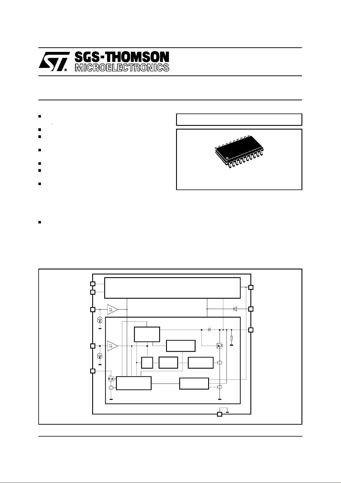
BLOCK DIAGRAM
IN1
DIAG1
S
Channel 1
MULTIPOWERBCD TECHNOLOGY
SO20 (12+4+4)
ORDERING NUMBER: L9386MD
DESCRIPTION
The L9386MD is a monolithic integrated dual low
side driver realized in an advanced MultipowerBCD mixed technology. It is especially intended
to drive valves in automotive environment. Its inputs are µP compatible for easy driving.Particular
care has been taken to protect the device
against failures, to avoid electro-magnetic interferences and to offer extensive real time diagnostic.
OUT1
VS
OUT2
DIAG2
IN2
EN
Diagnostic
Control
Output
Control
R
QS
Delay
Timer
Overtemp
Overload
Openload
R
O
Channel 2
GND
January 1995
This is advanced information on a new product now in development or undergoing evaluation. Details are subject to change without notice.
1/10
L9386MD
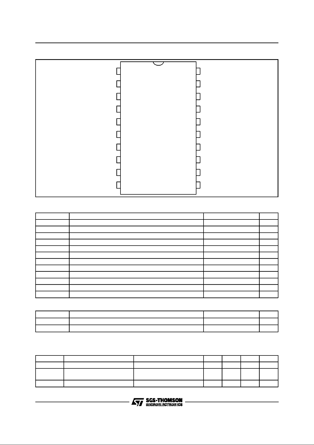
PIN CONNECTION(Top view)
IN1
DIAG2
OUT2
GND
GND
GND
GND
N.C.
EN
VS
ABSOLUTE MAXIMUM RATINGS
1
2
3
4
5
6
7
8
9
10
(no damage or latch)
IN2
20
DIAG1
19
OUT1
18
GND
17
GND
16
GND
15
GND
14
N.C.
13
N.C.
12
N.C.
11
Symbol Parameter Value Unit
VS
DC
VS
TR
V
IN,EN
VD
DC
VO
DC
VO
TR
I
O
I
OR
EO Switch-off energyfor inductive loads (t
T
jEO
T
j
T
a
DC supply voltage -16 to 45 V
Transient supply voltage ( t ≤ 500ms ) 60 V
Input voltage ( | ≤ | 10mA | ) -1.5 to 6 V
Diagnostic DC output voltage ( |≤| 50mA | ) -0.3 to 16 V
DC output voltage 45 V
Transient output voltage ( R
)60V
≥4Ω
L
Output load current internal limited
Reverse outputcurrent limited by load -4 A
= 250µs, T = 5ms) 50 mJ
EO
Junction temperature during switch-off ∑t = 30min 175 °C
Junction temperature -40 to +150 °C
Storage temperature -55 to +150 °C
THERMAL DATA
Symbol Parameter Value Unit
T
jDIS
R
th j-pins
ELECTRICAL CHARACTERISTICS
Thermal disable junction temperature threshold 160 to 190
Thermal resistance junction to pins 14
(Operating Range) - The electrical characteristics are valid within
the below defined operative range, unless otherwise specified.
Symbol Parameter Test Condition Min. Typ. Max. Unit
2/10
V
S
V
D
T
j
Board supply voltage 4.5 12 32 V
Stabilized diagnostic output
-0.3 5 16 V
voltage
Junction Temperature -40 150 °C
°
C/W
°
C
L9386MD
ELECTRICALCHARACTERISTICS
(continued)
Symbol Parameter Test Condition
IS
SB
Static standby supply current b)
c) V
EN
=L,VO≤VO
IS DC supply current b)
VD
ID
LE
Diagnostic ouput low voltage b) ID= 2mA
L
Diagnostic output leakage
current
ID Diagnostic output current
c) V
EN=VIN
c) I
D
VS = 0V or VS = open;
VD = 5.5V T
VD ≤ 16V DIAG = L 2 6 30 mA
= 1mA
=H
≤
j
capability
VO
UV
VO
∆
UV1,2
Open load voltage threshold VEN=X,VIN= L 0.51
Open load difference voltage
threshold
b) VEN = X, V
VS ≥ VO
C
≥ VO
IN1,2
VOC= output voltage of other
channel
c)
IO
UC
Open load current threshold a) VEN=VIN=H
c)
IO
VO
S
ON,OFF
R
R
DSON
V
(EN,IN)L
OC
IO
Over load current threshold b) 5 7 A
Output voltage during clamping IO
CL
100mA 45 52 60 V
≥
CL
Output (fall, rise) slew rate a) Fig. 2 200 1500 3200 V/ms
Internal output pull down resistor VEN= L 10 20 40 KΩ
Output on resistance VS > 9.5V IO = 2A
T
=25°C
j
T
= 150°C
j
Logic input low voltage |I
EN, IN
|≤10mA
b)
c)
V
(EN,IN)H
V
(EN,IN)hys
I
EN
I
IN
t
DON
t
D OFF
t
D H-L, Diag.
t
D IOu
t
DOL
Logic input high voltage 2.2 5.5 V
Logic input hysteresis 0.2 0.4 1 V
Enable input sink current 1V≤V
Logic input sink current 1V≤V
5.5V 10 30 60
≤
EN
5.5V 40 95 180
≤
IN
Output delay ON time a) Fig. 2 4 25
Output delay OFF time a) Fig. 2 5 15 30 µs
Diag. delay output OFF time a) Fig. 2 5 30 65 µs
Diagnostic open load delay time a) Fig. 4 8 50 µs
Diagnostic overload delay
a) Fig. 1 50 160 300 µs
switch-off time
125°C
=L
UV
Value
T
j1
Unit
Min. Typ. Max.
0.73 1.5
uv
15
1.3 5
15
mA
mA
mA
mA
0.35 0.5 V
0.1 2 µA
xVS
VO
0.9V
VO
0.7V
100
20
-1.5
-1.5
0.55
xVS
-
VO
C
1.25V
VO
-
C
1.25V
320 480 mA
200 300
0.59
V
xVS
-
VO
C
C
1)
-
V
1.6V
VO
-
C
C
V
-
1.8V
mA
mΩ
500
1
0.5
m
Ω
V
V
A
µ
A
µ
s
µ
a) 9V ≤ VS≤16V (Nominal operating range)
R
≤ 6Ω,
L
≤ IO
I
O
b) 6.5V ≤ VS≤ 16V(Diagnostic operation range)
c) 4.5V ≤ V
1) Limit under evaluation.
OC
< 6.5V and 16V < VS≤ 32V (Extended operation range)
S
3/10
 Loading...