

TRIPLE HIGH-SIDE MOSFET DRIVER
OVERVOLTAGE CHARGE PUMP SHUT OFF
FOR V
REVERSE BAT TER Y PR OTEC TI ON ( REFER RING TO THE APPLICATION CIRCUIT DIAGRAM)
PROGRAMMABLE OVERLOAD PROTECTION FUNCTION FOR CHANNEL 1 AND 2
OPEN GROUND PROTECTION FUNCTION
FOR CHANNEL 1 AND 2
CONSTANT GATE CHARGE/DISCHARGE
CURRENT
> 25V
VS
L9380
DESCRIPTION
The L9380 device is a controller for three external
N-channel power MOS transistors in "High-Side
Switch" configuration. It is intended for relays replacement in automotive electric control units.
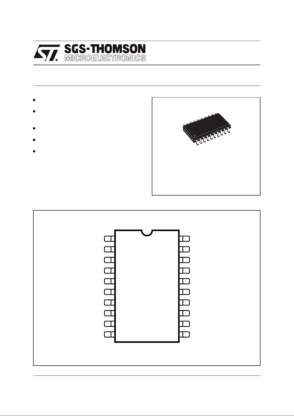
PIN CONNECTION (Top view)
T1
VS
N.C.
T2
PR
IN3
IN2
2
3
4
5
6
7
ORDERING NUMBER:
20
19
18
17
16
15
14
CP1
D1
N.C.
D2
G1
S1
S2
SO20
L9380
April 1998
IN1
EN G2
GND G3
8
9
10
13
12
11
D98AT391
N.C.
1/12
L9380
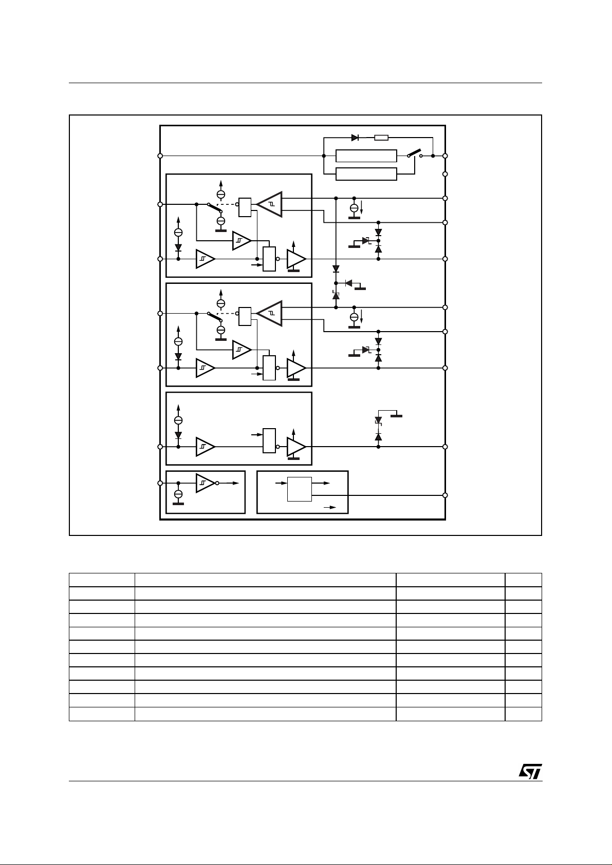
BLOCK DIAGRAM
VS
IN1
IN2
IN3
CHARGE PUMP
OVERVOLTAGE
VSI
T1
VSI
DRI VER 1
VSI
T2
VSI
DRI VER 2
VSI
DRI VER 3
≥1
ENN
≥1
ENN
ENN
-
+
CP
≥1
-
+
CP
≥1
CP
≥1
IPR
IPR
CP
GND
D1
S1
G1
D2
S2
G2
G3
EN
ENN
VS VSI
REG.
2V
I
REFERENCE
PR
PR
D98AT390
ABSOLUTE MAXIMUM RATINGS
Symbol Parameter Value Unit
V
S
V
S
/dt Supply Voltage slope -10 to +10 V/µs
V
∆
S
V
IN,EN
V
T
V
D, G, S
V
D, G, S
I
D, G, S
T
j
T
stg
Note: ESD for all pins, except the timer pins, are according to MIL 883C, tested at 2KV, corresponds to a maximum energy dissipation of 0.2mJ.
The timer pins are tested with 800V
2/12
DC Supply Voltage -0.3 to +27 V
Supply Voltage pulse (t ≤ 400ms) 45 V
Input / Enable Voltage -0.3 to +7 V
Timer Voltage -0.3 to 27 V
Drain, gate, source voltage -15 to +27 V
Drain, gate, source voltage pulse (t ≤ 400ms) 45 V
Drain, gate, source current (t ≤ 2ms) 0 to +4 mA
Operating Junction Temperature -40 to 150 °C
Storage Temperature -65 to 150 °C
THERMAL DATA
Symbol Parameter Value Unit
R
th j-amb
Thermal Resistance Junction to Ambient 100 °C/W
LIFETIME
Symbol Parameter Condition Value Unit
t
B
t
b
Useful life time VS = 0V 20 years
Operating life time VS = 7 to 18.5V 5000 hours
PIN FUNCTIONS
N. Name Function
1 T1 Timer capacitor; the capacitor defines the time for the channel 1 shut down, after overload of
2V
4 T2 Timer capacitor; the capacitor defines the time for the channel 2 shut down, after overload of
5 PR Programming resistor for overload detetcion threshold; the resistor from this pin to ground
6 IN3 Input 3; equal to IN1.
7 IN2 Input 2; equal to IN1.
8 IN1 Input 1; logic signal applied to this pin controls the driver 1; this pin features a current source to
9 EN Enable logic signal high on this pin enables all channels
10 GND Ground
11 G3 Gate 3 driver output; current source from CP or ground
12 G2 Gate 2 driver output; current source from CP or ground
14 S2 Source 2 sense input; monitors the source voltage.
15 S1 Source 1 sense input; monitors the source voltage.
16 G1 Gate 1 driver output; current source from CP or ground
17 D2 Drain 2 sense input; a programmable input bias current defines the drop across the external
19 D1 Drain 1 sense input; a programmable input bias current defines the drop across the external
20 CP Charge pump capacitor; a alternating current source at this pin charges the connected
3, 13, 18 NC Not connected
the external MOS transistor has been detected.
Supply Voltage.
S
the external MOS transistor has been detected.
defines the drain pin current and the charging of the timer capacitor.
assure defined high status when the pin is open.
resistor RD1; this drop fixes the overload threshold of the external MOS.
resistor R
capacitor C
; this drop fixes the overload threshold of the external MOS.
D1
to a voltage 10V higher than VS; the charge stored in this capacitor is thanused
CP
to charge all the three gates of the power MOS transistors.
L9380
3/12
L9380
ELECTRICAL CHARACTERISTICS (7V ≤ V
≤ 18.5V; -40°C ≤ TJ ≤ 150°C, unless otherwise specified.)
S
Symbol Parameter Test Condition Min. Typ. Max. Unit
SUPPLY
I
VS
Static Operating Supply Current VS = 14V 2.5 mA
CHARGE PUMP
V
CP
t
CP
V
SCP off
V
SCP hys
f
CP
Charge Pump Voltage Above V
S
817V
Charging Time VCP = VS + 8V CCP = 100pF 200
Overvoltage Shut down 20 30 V
Overvoltage Shut down
Hysteresis
1)
Charge Pump frequency
1)
50 200 1000 mV
100 250 400 KHz
s
µ
GATE DRIVERS
I
GSo
I
GSi
Gate Source Current VG = V
S
-5 -3 -1 mA
Gate Sink Current VG ≥ 0.8V 1 3 5 mA
DRAIN - SOURCE SENSING
V
PR
Bias Current Programming
10µA ≤ IPR ≤ 100µA; VD ≥ 4V 1.8 2 2.2 V
voltage
I
D Leak
I
I
Smax
V
HYST
D
Drain pin leakage current VS = 0V; VD =14V 0 5
Drain pin bias current VS ≥ VD + 1V; VD ≥ 5V 0.9 I
PR
1.1 I
Source pin input current VS ≥ VD + 1V; VD ≥ 7V 10 60
µ
PR
µ
Comparator Hysteresis 20 mV
A
A
TIMER
V
THi
V
TLo
I
T
Timer threshold high 4 4.4 4.8 V
Timer threshold low 0.3 0.4 0.5 V
Timer Current IN = 5V; VT = 2V
IN = 0V; V
V
≥ 5V; VT = 2V
D
< VD;
S
0.4 I
-0.6 I
PR
PR
0.6 I
-0.4 I
PR
PR
INPUTS
V
LOW
V
HIGH
V
INhys
I
IN
I
EN
t
d
NOTE: Not measured guaranteed by design
Input Enable low voltage -0.3 1 V
Input Enable high voltage 3 7 V
Input Enable Hysteresis
Input source current VIN ≤ 3V -30 -5
Enable sink current VEN ≥ 1V 5 30
(1)
50 200 500 mV
µ
µ
Transfer time IN/ENABLE VS = 14V VG = VS; OPEN GATE 2.5
A
A
s
µ
Function is given for supply voltage down to 5.5V. Function means: The channels are controlled from the
inputs, some other parameters may exceed the limit. In this case the programming voltage and timer
threshold will be lower. This leads to a lower protection threshold and time.
FUNCTIONAL DESCRIPTION
The Triple High-Side Power-MOS Driver features
all necessary control and protection functions to
switch on three Power-MOS transistors operating
as High-Side switches in automotive electronic
control units. The key application field is relays replacement in systems where high current loads,
usually motors with nominal currents of about 40A
connected to ground, has to be switched.
A high signal at the EN pin enables all three
channels. With enable low gates are clamped to
ground. In this c ondition the gate sink current is
higher than the specified 3mA. An enable low sig-
4/12
nal makes also a reset of the timer.
A low signal at the inputs switch on the gates of
the external MOS. A short circuit at the input
leads to permanent activation of the concerned
channel. In this case the device can be disabled
with the enable pin. The charge pump loading is
not influenced due to the enable input.
An external N-channel MOS driver in high side
configuration needs a gate driving voltage higher
than V
. It is generated by means of a charge
S
pump with integrated charge transfer capacitors
and one external charge storage capacitor C
CP
The charge pump is dimensioned to load a ca-
.

Figure 4. Timing Characteristic.
V
IN
V
G
L9380
t
d
V
S
V
T
4.4V
0.4V
pacitor CCP of 33nF in less than 20ms up to 8V
above V
. The value of CCP depends on the input
S
capacitance of the external MOS and the decay
of the charge pump voltage down to that value
where no significant influence on the application
occurs.
The necessary charging time for C
has to be
CP
respected in the sequence of the input control signals. As a consequence the lo wer gate to source
voltage can cause a higher drop across the
Power-MOS and get into overload condition. In
this case the overload protection timer will start.
After the protection time the concerned channel
will be switched off. Channel 3 is not equipped
with an overload protection. The same situation
can occur due to a discharge of the storage capacitor caused by the gate s hort to ground. The
gate driver that is supplied from the pin CP, which
is the charge pump output, has a sink and source
current capability of 3mA. For a short-circuit of the
load (source to ground) the L9380 has no gate t o
source limitation. The gate source protection must
be done externally.
Channel 1 and 2 provide drain to source voltage
sensing possibility with programmable shut-off
delay when the activation threshold was exceeded. This threshold V
nal resistor R
. The bias current flowing through
D
is set by the exter-
DSmin
this resistor is determined by the programming re-
t
d
V
DSmin
T
off
D98AT392
Figure 5. Drain, source input current.
I
D
IPR + I
sistor R
Dmax
V
D
> V
S
I
PR
0
. This external resistor RPR defines also
PR
D98AT393
V
V
S
S
D
= V
> V
D
the charge and discharge current of the timer capacitor C
and the timer shut off delay time T
. The drain to source threshold V
CT
off
culated:
min = VPR (RD /RPR)
V
DS
T
= 4.4 CT R
off
PR
I
SmaxIS
DSmin
can be cal-
5/12

L9380
In application which don’t use the overload protection or if one channel is not used, the Timer pin
of this channel must be connected to ground and
bat
the drain pin with a resistor to V
.
The timing characteristic illustrates the function
and the meaning of V
DSmin
and T
(see figure 4).
off
The input current of the overload sense comparator is specified as I
. The sum IPR + I
Smax
erates a drop across the external resistor R
Dmax
gen-
if
D
the drain pin voltage is higher than the source pin
(see Fig. 5). In the switching point the comparator
input source pin currents are equal and the half of
the specified current I
sation equal external resistors (R
. For an offset compen-
Smax
= RS) at drain
D
and source pin are imperative. The drain sense
comparator, which detects the overload, has a
symmetrical hysteresis of 20mV (see Fig. 6). Exceeding the source pin voltage by 10mV with respect to the drain voltage forces the timer capacitor to discharge. Decreasing the source pin
voltage 10mV lower than the drain pin voltage an
overload of the external MOS is detecte d and the
timer capacitor will be loaded. After reaching a
voltage at pin CT higher than t he timer threshold
the influenced channel is switched off . In this
V
Thi
case the overload is stored in the timer capacitor.
The timer capacitor will be discharged with a
’High’ signal at the input (see Fig. 4). After r eaching the lower timer threshold V
the overload
TLo
protection is reset and the channel is able to
switch on again.
The application diagram is shown in Fig. 7. Because of the transients present at the power lines
during operation and possible disturbances in the
system the external resistors are necessary.
Positive ISO-Pulses at Drain, Gate Source are
clamped with an active clamping structure. The
clamping voltage is less than 60V. Negative
Pulses are only clamped with the ESD-Structure
less than -15V. This transients lower than -15V
can influence the other channels.
In order to protect the transistor against overload
and gate breakdown protection diodes between
gate and source and gate and drain has to be
connected. In case of overvoltage into V
(VS >
S
20V) the charge pump oscillation is stopped.
Then the charge pump capacitor will be loaded by
Figure 6. Comparator hysteresis.
V
T
D98AT394
-10mV
a diode and a resistor in series up to V
V
Dr
+10mV
V
S
So
(see
Block Diagram). In this case the channels are not
influenced. In reverse battery condition the pins
D1, D2, S1, S2 follow the battery potential down
to -13V (high impedance) and the gat e dr iv er pins
G1, G2 is referred to S1, S2. In this way it is assured that M1 and M2 will not be driven into the
linear conductive mode. This protection function
is operating for V
, VS2 down to -15V. The gate
S1
driver output G3 is referred to the D1 in this case.
This function guarantees that the source to
source connected N-Channel MOS transistors M3
and M4 remains OFF.
All the supplies and the in- and output of the PCBoard are supplied with a 40 wires flat cable (not
used wires are left open). This cable is submitted
to the RF in the strip-line like described in DIN
40839-4 or ISO 11456-5.
The measured circuit was build up on a PCB
board with ground plane. In t he frequency range
from 1MHz to 400MHz and 80% AM-modulation
of 1KHz with field strength of 200V/m no influence
to the basic function was detected on a typical device. The failure criteria is an envelope of the output signal with 20% in the amplitude and 2% in
the time.
6/12

Figure 7. Application Circuit.
L9380
D1
V
BAT
MICROCONTROLLER
C1D2
C2
C3
VS
T1
IN1
T2
IN2
IN3
EN
VSI
VSI
DRIVER 1
VSI
VSI
DRIVER 2
VSI
DRIVER 3
LOAD CONTROL
≥1
ENN
≥1
ENN
ENN
ENN
+
CP
≥1
+
CP
≥1
CP
≥1
VS VSI
REG.
2V
REFERENCE
I
CHARGE PUMP
OVERVOLTAGE
PR
CP
GND
D1
IPR
G1
S1
D2
IPR
G2
S2
G3
PR
C4
R1
D3
R2
D4
R3
R4
D5
R5
D6
R6
D7
R7
R8
VALUE DRIVER
U405
M1
M2
MM1
M3
D8
M4
MM2
L4L3L2L1
D98AT395
Recommendations to the application circuit: The timer and the charge capacitors are loaded wit h an alternating current source. A short ground connection of the charge capacitor is indispensable to avoid
electromagnetic emigrations. The dimension of the resistors RD, RG and RS have to respect the maximum current during transients at each pin.
7/12

L9380
TYPICAL CHARACTERISTICS
Depending on production spread, certain deviations may occure. For limits (see pag. 4)
Figure 8. Charge Loading Time as function of V
(Vcp = 8V +VS)
t
CH
(ms)
20
10
0
68nF
33nF
10nF
6 10121416VS(V)8
D98AT396
Figure 10. Ground Loss Protection Gate Dis-
carge Current for Source Voltage
I
(µA)
-200
G
D98AT398
Figure 9. Charge Pump Current as function of
S
the Charge Voltage
I
CP
(µA)
100
10V
50
7V
0
71727V
12V
16V
Figure 11. Input Current as function of the Input
Voltage
I
C
(µA)
-5
D98AT397
D98AT399
(V)
C
-400
-600
-800
-1000
-15 -10 -5 VS(V)
Figure 12. Overvoltage Shutdown of the Charge
Pump with Hysteresis
V
CH
(V)
30
20
24 24.5 25 25.5 VS(V)
D98AT400
-10
-15
-20
01234V
(V)
I
8/12

Figure 13. Measured Circuit.
The EMS of the device was verified in the below described setup.
3.125Hz
9
6.25Hz
12.5Hz
25Hz
BAT
8
7
6
1V
345 10 12
U(t)
BNC
+
CAR-BATTERY
2m
STRIPLINE
f
2
f
2
f
2
L9380
ANECHOIC CHAMBER
SMB7W01-200
2V
BNC
S
100nF
1KΩ
6IN1
2.2nF
5.6V 4.7nF
IN2
IN3
EN
1KΩ
7
2.2nF
1KΩ
8
2.2nF
1KΩ
9
2.2nF
5.6V
10
PC-BOARD IN RF BOX
4.7nF5.6V
4.7nF5.6V
4.7nF
33µFSMT_39A
10nF
10nF
VS
T1
IN1
T2
IN2
IN3
EN
VSI
VSI
DRIVER 1
VSI
VSI
DRIVER 2
VSI
DRIVER 3
ENN
≥1
ENN
≥1
ENN
ENN
REFERENCE
-
+
CP
≥1
-
+
CP
≥1
CP
≥1
VS VSI
REG.
2V
I
PR
CHARGE PUMP
OVERVOLTAGE
IPR
IPR
CP
GND
2KΩ
D1
STD17N06
G1
10KΩ
2KΩ
S1
2KΩ
D2
STD17N06
G2
10KΩ
S2
2KΩ
STD17N06
G3
10KΩ
20KΩ
PR
33V
18V
1KΩ
33V
18V
1KΩ
33V
33nF
18V
5Ω
B60N06
5Ω
B60N06
10KΩ
10KΩ
B60N06
10KΩ
1KΩ
3
4
5
OUT1
2.2nF
OUT2
2.2nF
OUT3
2.2nF
D98AT401
9/12

L9380
Figure 14: PCB Board
Electromagnetic Emission Classi f icat ion (EME)
Electromagnetic Emission classes presented below are typical data found on bench te st. For detailes
test description please refer to "Electromagnetic Emission (EME) Measurement of Integrated Circuits,
DC to 1GHz" of VDE/ZVEI work group 767.13 and VDE/ZVEI work group 767.14 or IEC project number
47A 1967Ed. This data is targeted to board designers to allow an estimation of emission filtering effort
required in application. All measurements are done with the EMS-board (See pages 9, 10)
Pin EME class Remark
VCP G - w
Electromagnetic Emission and Susceptivity is not tested in production.
10/12

SO20 PACKAGE MECHANICAL DATA
L9380
DIM.
MIN. TYP. MAX. MIN. TYP. MAX.
A 2.35 2.65 0.093 0.104
A1 0.1 0.3 0.004 0.012
B 0.33 0.51 0.013 0.020
C 0.23 0.32 0.009 0.013
D 12.6 13 0.496 0.512
E 7.4 7.6 0.291 0.299
e 1.27 0.050
H 10 10.65 0.394 0.419
h 0.25 0.75 0.010 0.030
L 0.4 1.27 0.016 0.050
K 0 (min.)8 (max.)
mm inch
L
A
B
e
K
D
1120
E
110
SO20MEC
h x 45˚
A1
H
C
11/12

L9380
Information furnis hed is believe d to be ac curate and reliabl e. However, SGS-THOMS ON Mi croelectroni cs as sumes no res ponsib ility for the
consequences of use of such information nor for any infringement of patents or other rights of third parties w hi ch may result from i ts use. No
license is granted by implication or otherwise under any patent or patent rights of SGS-THOMSON Microelectronics. Specification mentioned
in this p ublication are subject to c hange w ithout not ice. T his pub lic ation super sedes a nd replaces all informa tion previous ly supplied. SGSTHOMSON Mic roelectronics products are not author ized for use as cri tical components in l ife support devices or systems with out express
written approval of SGS-THOMSON Microelectronics.
© 1998 SGS-THOMSON Microelectronics – Printed in Italy – All Rights Reserved
SGS-THOMSON Microelectronics GROUP OF COMPANIES
Australia - Brazil - Canada - China - France - Germany - Italy - Japan - Korea - Malaysia - Malta - Morocco - The Netherlands -
Singapore - Spain - Sweden - Switzerland - Taiwan - Thailand - United Kingdom - U.S.A.
12/12
 Loading...