

1/21
L9352
June 2002
■
Quad low-side switch
■
2 x 5A designed as conventional switch
■
2 x 2.5A designed as switched current-regulator
■
Low ON-resistance 4 x 0.2Ω (typ.)
■
Power SO-36 - package with integrated
cooling area
■
Integrated free-wheeling and clamping Z-diodes
■
Output slope control
■
Short circuit protection
■
Selective overtemperature shutdown
■
Open load detection
■
Ground and supply loss detection
■
External clock control
■
Recirculation control
■
Regulator drift detection
■
Regulator error control
■
Regulator resolution 5mA
■
Status monitoring
■
Status push-pull stages
■
Electrostatic discharge (ESD) protection
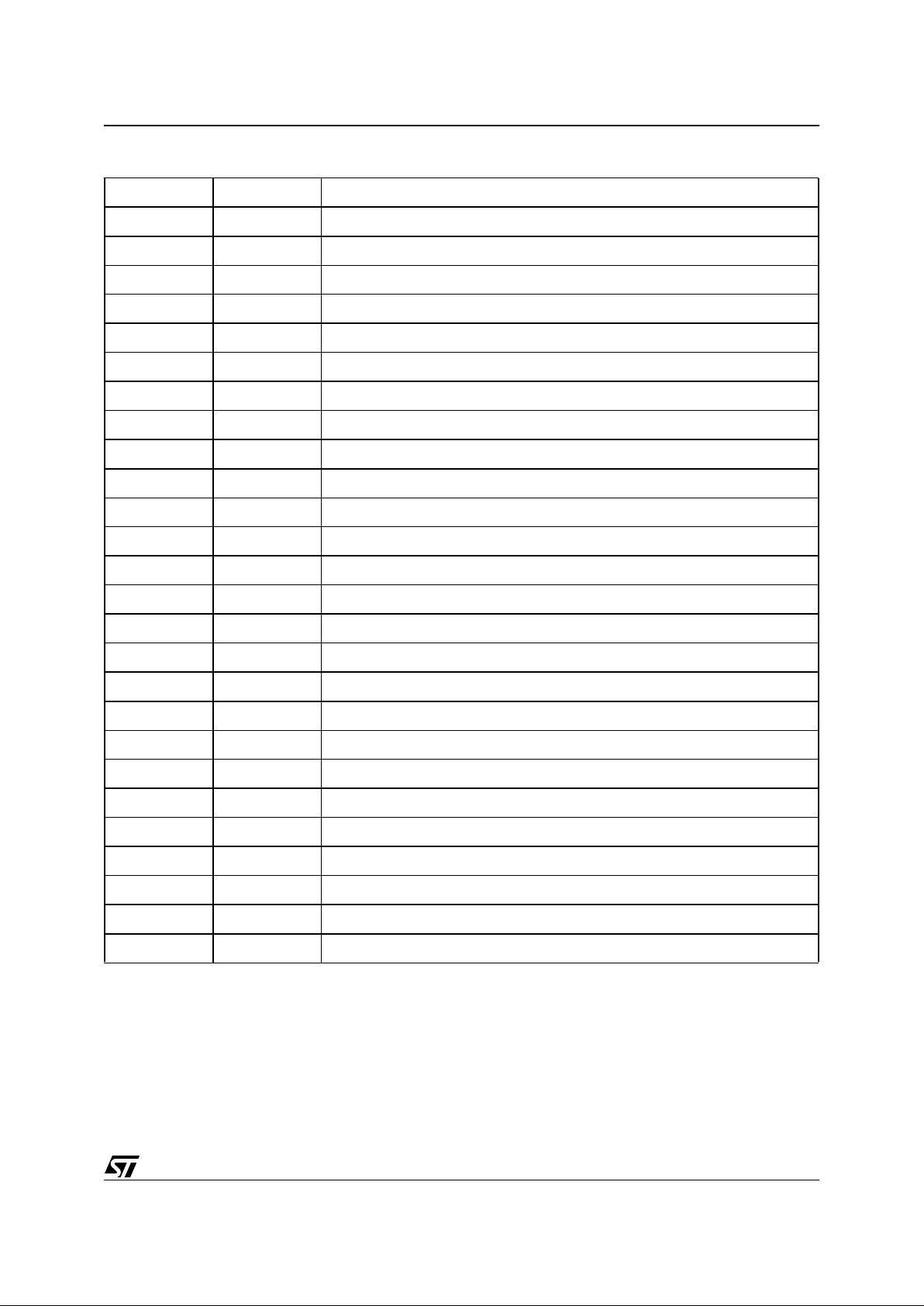
DESCRIPTION
The L9352 is an integrated quad low-side power
switch to drive inductive loads like valves used in
ABS systems. Two of the four channels are current
regulators with current range from 250mA to 2.25A
and an accuracy of 10%.
All channels are protected against fail functions.
They are monitored by a status output.
Figure 1. Pin Connection
36
N.C.
35
IN3
ST4
34
PGND3
33
32
PGND3
Q3
31
Q3
30
29
D3
D3
28
Q2
27
26
Q2
PGND2
25
PGND2
24
23
VS
VDD
22
VCC
21
20
IN2
ST1
19
GND 1
IN4
2
3
ST3
PGND4
4
PGND4
5
6
Q4
Q4
7
D4
8
9
D4
Q1
10
Q1
11
12
PGND1
PGND1
13
EN
14
15
CLK
IN1
16
ST2
17
18
TEST
99AT0060
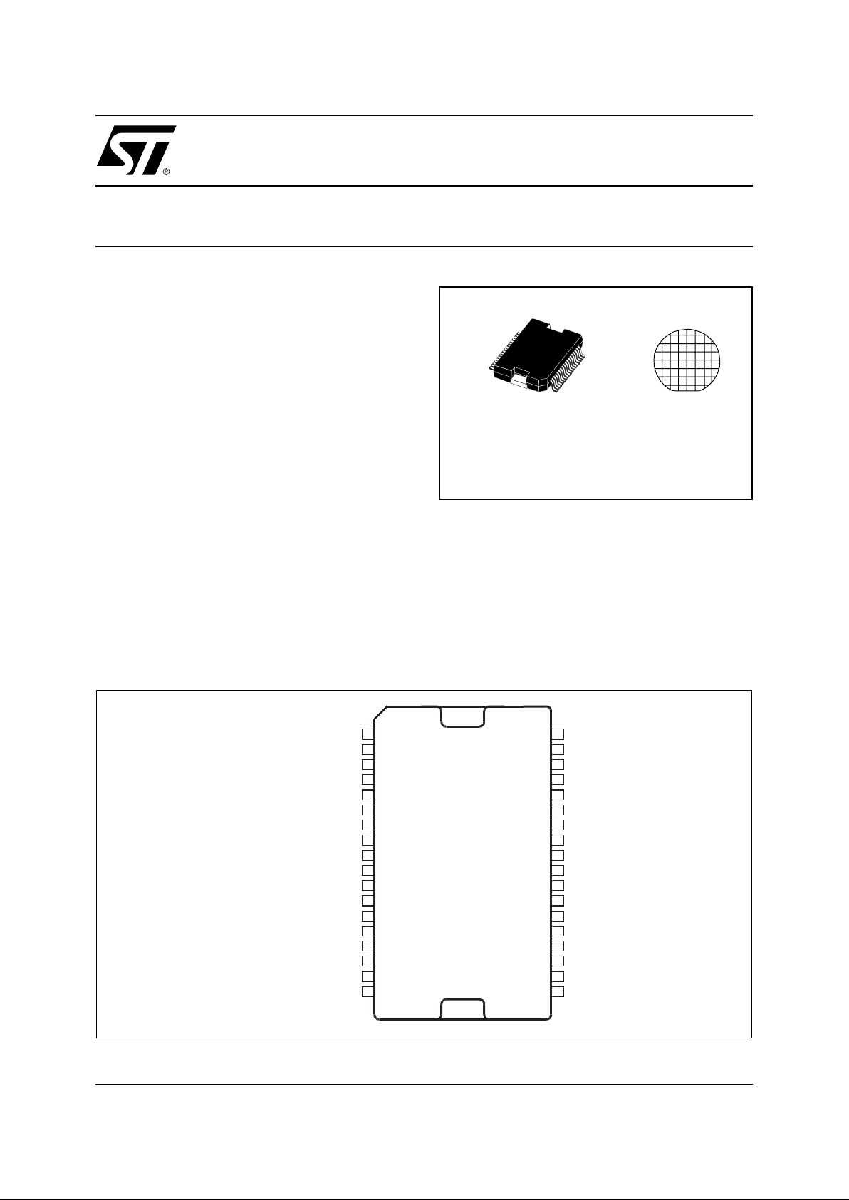
PowerSO-36 BARE DIE
ORDERING NUMB ERS :
L9352 L9352-DIE1
INTELLIGENT QUAD (2X5A/2X2.5A) LOW-SIDE SWITCH
L9352
2/21
Figure 2. Block Diagram
99AT0059
LOGIC
Overload
Open Load
GND-det.
Overtemperature
Channel 1
Overtemperature
Channel 4
LOGIC
&
DA
Overload
Open Load
GND-det.
IPD
IPD
LOGIC
Overload
Open Load
GND-det.
Overtemperature
Channel 2
Overtemperature
Channel 3
LOGIC
&
DA
Overload
Open Load
GND-det.
IPD
IPD
drift-det.
VS VCC VDD
Q1
D4
Q4
Q2
D3
Q3
GND
TEST
ST3
IN3
ST2
IN2
ST4
IN4
ST1
IN1
CLK
EN
Internal Supply
3/21
L9352
PIN DESCRIPTION
N° Pin Function
1 GND Logic Ground
2, 3 PGND 3 Power Ground Channel 3
4, 5 Q 3 Power Output Channel 3
6, 7 D 3 Free-Wheeling Diode Channel 3
8, 9 Q 1 Power Output Channel 1
10, 11 Q 2 Power Output Channel 2
12, 13 D 4 Free-Wheeling Diode Channel 4
14, 15 Q 4 Power Output Channel 4
16, 17 PGND 4 Power Ground Channel 4
18 NC Not Connected
19 VCC 5V Supply
20 VDD 5V Supply
21 ST 4 Status Output Channel 4
22 IN 2 Control Input Channel 2
23 IN 4 Control Input Channel 4
24 ST 2 Status Output Channel 2
25 EN Enable Input for all four Channels
26 TEST Enable Input for Drift detection
27, 28 PGND 2 Power Ground Channel 2
29 VS Supply Voltage
30, 31 PGND 1 Power Ground Channel 1
32 ST 1 Status Output Channel 1
33 IN 3 Control Input Channel 3
34 IN 1 Control Input Channel 1
35 ST 3 Status Output Channel 3
36 CLK Clock Input
L9352
4/21
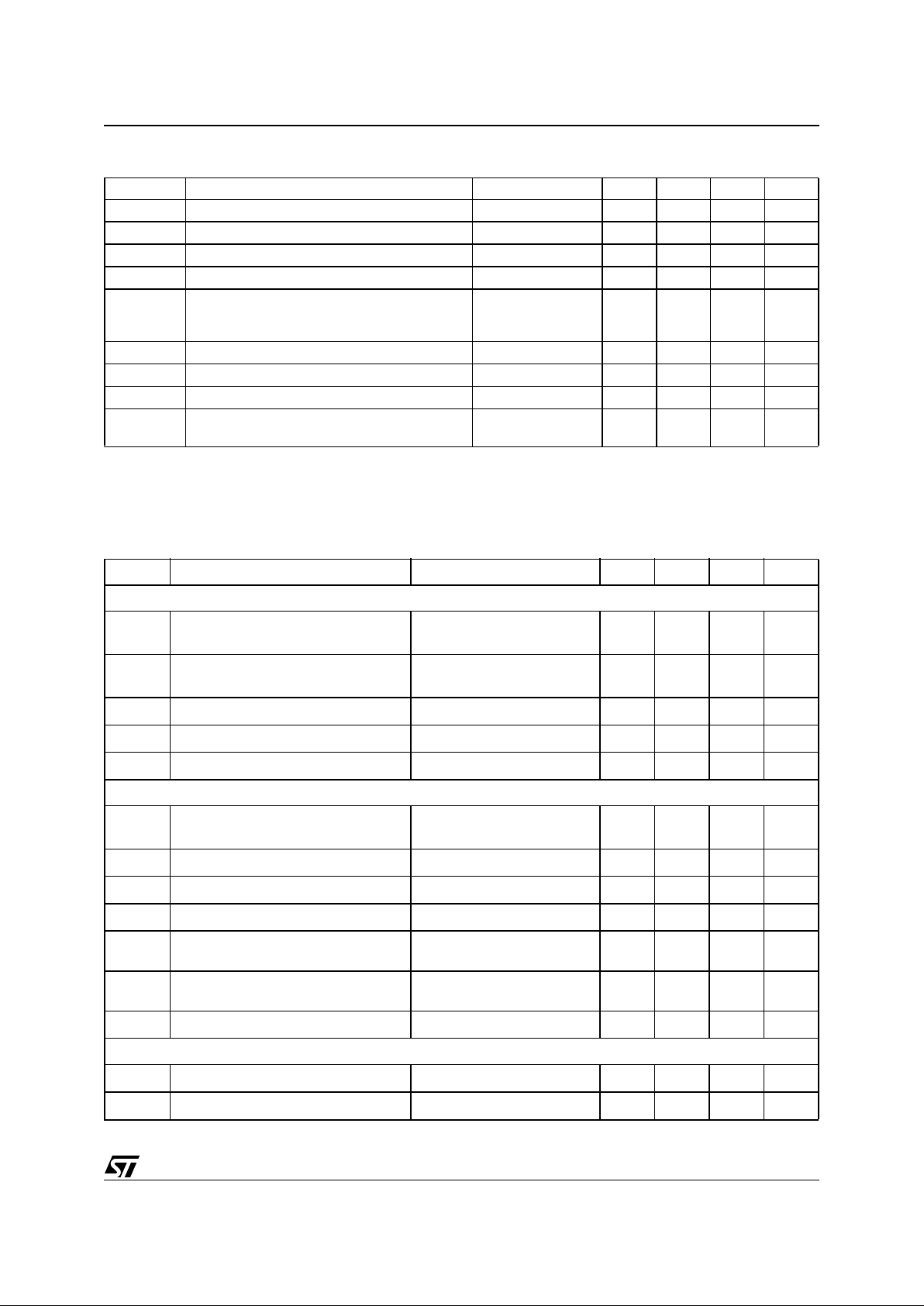
ABSOLUTE MAXIMUM RATINGS
The absolute maximum ratings are the limiting values for this device. Damage may occur if this device is subjected to conditions which are beyond these values.
THERMAL DATA
Symbol Parameter Test Conditions Min Typ Max Unit
E
Q
Switch off energy for inductive loads 50 mJ
Voltages
V
S
Supply voltage -0.3 40 V
V
CC
, V
DD
Supply voltage -0.3 6 V
V
Q
Output voltage static 40 V
V
Q
Output voltage during clamping t < 1ms 60 V
V
IN
, V
EN
Input voltage IN1 to IN4, EN II < |10|mA -1.5 6 V
V
CLK
Input Voltage CLK -1.5 6 V
V
ST
Output voltage status -0.3 6 V
V
D
Recirculation circuits D3, D4 40 V
V
DRmax
max. reverse breakdown voltage of free
wheeling diodes D3, D4
55 V
Currents
I
Q1/2
Output current for Q1 and Q2 >5
internal
limited
A
I
Q3/4
Output current for Q3 and Q4 >3
internal
limited
A
I
Q1/2
,
I
PGND1/2
Output current at reversal supply for Q1
and Q2
-4 A
I
Q3/4
,
I
PGND3/4
Output current at reversal supply for
Q3 and Q4
-2 A
I
ST
Output current status pin -5 5 mA
ESD Protection
ESD Elec trost atical Disch argin g
GND, PGND, Qx, Dx, CLK, ST, IN,
TEST, EN
MIL883C ±2kV
VS,
VCC,VDD
Supply pins vs. GND and PGND ±1 kV
ESD Output Pins (Qx, Dx) vs. Common GND
(PGND1-4 + GND)
±4kV
Symbol Parameter Test Conditions Min Typ Max Unit
T
j
Junction temperature T
j
-40 150 °C
T
jc
Junction temperature during clamping
(life time)
Σ
t = 30min
Σ
t = 15min
175
190
°C
T
stg
Storage temperature T
stg
-55 150 °C
T
th
Overtemperature shutdown threshold
(1)
(1) This parameter will not be tested but assured by design
175 200 °C
T
hy
Overtemperature shutdown hysteresis
(1)
10 °C
R
thJC
Thermal resistance junction to case R
thJC
2 K/W
5/21
L9352
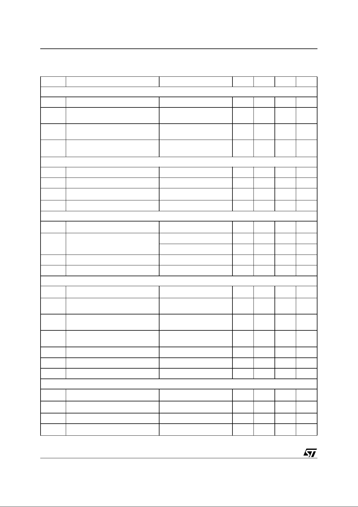
OPERATING RANGE
.
Symbol Parameter Test Conditions Min. Typ. Max. Unit
V
S
Supply voltage 4.8 18 V
V
CC
, V
DD
Supply voltage 4.5 5.5 V
dV
S
/dt Supply voltage transient time -1 1
V/
µ
s
V
Q
Output voltage static -0.3 40 V
V
Q
Output voltage induced by inductive switching Voltage will be
limited by internal
Z-diode clamping
60 V
V
ST
Output voltage status -0.3 6 V
I
ST
Output current status -1 1 mA
T
j
Junction temperature -40 150 °C
T
jc
Junction temperature during clamping
Σ
= 30min
Σ
= 15min
175
190
°C
ELECTRICAL CHARACTERISTCS
:
(Vs = 4.8 to 18V; T
j
= -40 to 150°C unless otherwise specified)
Symbol Parameter Test Condition Min. Typ. Max. Unit
Power Supply
I
SON
Supply current
V
S
≤ 18V
(outputs ON)
5mA
I
SOFF
Quiescent current
V
S
≤ 18V
(outputs OFF)
5mA
I
cc
Supply current VCC (analog supply) VCC =5V 5 mA
I
dd
Supply current VDD (digital supply) VDD =5V f
CLK
=0Hz 5 uA
I
dd
Supply current VDD (digital supply) VDD =5V f
CLK
=250kHz 5 mA
General Diagnostic Functions
V
QU
Open load voltage
V
S
≥ 6.5V
(outputs OFF)
0.3 0.33 0.36 x V
Q
V
thGND
Signal-GND-loss threshold VCC= 5V 0.1 1 V
V
thPGL
Power-GND-loss thresh old VCC= 5V 1.5 2.5 3.5 V
f
CLK,min
Clock frequency error 10 100 kHz
DC
CLKe_l
ow
Clock duty cycle error detection low f
CLK
= 250 kHz 33,3 45 %
DC
CLKe_
high
Clock duty cycle error detection high f
CLK
= 250 kHz 55 66,6 %
VS
loss
Supply detection VCC = VDD = 5V 2 4.5 V
Additional Diagnostic Functions channel 1 and channel 2 (non regulated channels)
I
QU1,2
Open-load current channel 1, 2
V
S
≥ 6.5V
50 300 mA
I
QO1,2
Over-load current channel 1, 2
V
S
≥ 6.5V
57.59 A
L9352
6/21
Additional Diagnostic Functions channel 3 and channel 4 (regulated channels)
DC
OUT
Output duty cycle range filtered with 10ms 10 90 %
I
QO3,4
Overload current
channel 3,4
V
S
≥ 6.5V
2.5 5 8 A
V
rerr
Recirculation error shutdown
threshold (open D3/D4)
Iout > 50mA 45 50 60 V
PWM
dOU
T
Output PWM ratio during drift
comparison
V
IN3
= V
IN4
= PWM
IN
V
TEST
= H
-14.3 +14.3 %
Digital Inputs (IN1 to IN4, ENA, CLK, TEST). The valid PWM-Ratio for IN3/IN4 is 10% to 90%
V
IL
Input low voltage -0.3 1 V
V
IH
Input high voltage 2 6 V
V
IHy
Input voltage hysteresis
(1)
20 500 mV
I
I
Input pull down current
V
IN
= 5V, VS ≥ 6.5V
82040
µ
A
Digital Outputs (ST1 to ST4)
V
STL
Status output voltage in low state
(2))
IST ≤ 40µA
0 0.4 V
V
STH
Status output voltage in high state
(2)
IST ≥ -40µA
2.5 3.45 V
I
ST
≥ -120µA
23.45V
R
DIAGLROUT
+ R
DSON
in low state 0.3 0.64 1.5
k
Ω
R
DIAGHROUT
+ R
DSON
in high state 1.5 3.2 7.0
k
Ω
Power Outputs (Q1 to Q4)
R
DSON
Static drain-source ON-resistance
IQ = 1A; VS ≥ 9.5V
0.2 0.4
Ω
V
F_250mA
Forward voltage of free wheeling path
D3, D4 @250mA
I
D3/4
= -250mA 0.5 1.5 V
V
F_2.25A
Forward voltage of free wheeling path
D3, D4 @2.25A
I
D3/4
= -2.25A 2.0 4.5 V
R
sens
Sense resistor = (V
F_2.25A-VF_250mA
)/
2A
1
Ω
V
Z
Z-diode clamping voltage
I
Q
≥ 100mA
45 60 V
I
PD
Output pull down current VEN = H, VIN = L 10 150
µ
A
I
Qlk
Output leakage current VEN = L; VQ = 20V 5
µ
A
Timing
t
ON
Output ON delay time
I
Q
= 1A
0520
µ
s
t
OFF
Output OFF delay time channel
I
Q
= 1A
01030
µ
s
t
OFFREG
Output OFF delay time regulator
(3)
528
µ
s
t
r
Output rise time
IQ = 1A
0.5 1.5 8
µ
s
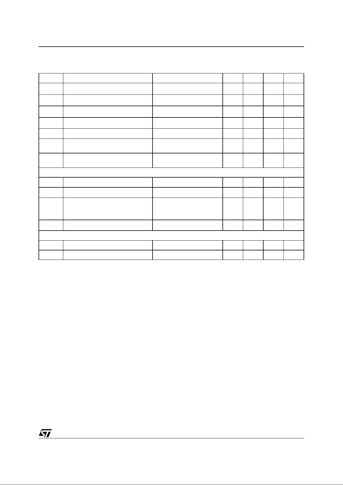
ELECTRICAL CHARACTERISTCS
:
(continued)
(Vs = 4.8 to 18V; Tj = -40 to 150°C unless otherwise specified)
Symbol Parameter Test Condition Min. Typ. Max. Unit
7/21
L9352
t
f
Output fall time
I
Q
= 1A
0.5 1.5 8
µ
s
t
sf
Short error detection filter time
f
CLK
= 250kHz DC = 50%
(3)
48
µ
s
t
lf
Long error detection filter time f
CLK
= 250kHz DC = 50%
(3)
16 32
µ
s
t
SCP
Short circuit switch-OFF delay time
(3)
430
µ
s
t
D
Status delay time
(3)
896 1024 us
t
RE
Regulation error status delay time
(3)
(reg. channels only)
10 ms
t
Dreg
Output off status delay time
(3)
(reg. channels only
528
µ
s
Reg. Current Accuracy (reg. channels only)
I
Q3/Q4
Minimum current DC = 10% 200 250 300 mA
I
Q3/Q4
Maximum current DC = 90% 2 2.25 2.5 A
I
REG
Max. regulation deviation @
DC 10% - 90%
250mA < I
Q3/Q4
< 400mA
400mA ≤ I
Q3/Q4
≤ 800mA
800mA < I
Q3/Q4
< 2.25A
±10
±6
±10
%
%
%
∆
I
Q3/Q4
Min. quant. step 5 mA
Frequencies
CLK frequency crystal-controlled 250 kHz
Input PWM frequency (reg. channels only) 2 kHz
(1) This parameter will not be tested but assured by design.
(2) Short circuit between two digital outputs (one in high the other in low state) will lead to the defined result "LOW"
(3) Digi t al filtered wit h external cloc k, only functional test
ELECTRICAL CHARACTERISTCS
:
(continued)
(Vs = 4.8 to 18V; Tj = -40 to 150°C unless otherwise specified)
Symbol Parameter Test Condition Min. Typ. Max. Unit

L9352
8/21
1.0 Functional Description
1.1 Overv iew
The L9352 is designed to drive inductive loads (relays, electromagnetic valves) in low side configuration. Integrated active Zener-clamp (for channel1 and 2) or free wheeling diodes (for channel 3 and 4) allow the recirculation of the inductive loads. All four channels are monitored with a status output. All wiring to the loads and
supply pins of the device are controlled. The device is self-protected against shor t circuit at the outputs and overtemperature. For each channel one independent push-pull status output is used for a parallel diagnostic function.
Channel 3 and 4 work as current regulator. A PWM signal on the input defines the target output current. The
output current is controlled through the output PWM of the power stage. The regulator limits of 10% or 90% are
detected and monitored with the status signal. The current is measured during recirculation phase of the load.
A test mode compares the differences between the two regulators. This “drift” test compares the output PWM
of the regulators. By this feature a drift of the load during lifetime can be detected.
1.2 In put Ci rc ui ts
The INput, CLK, TEST and ENable inputs, are active high, consist of Schmidt triggers with hysteresis. All inputs
are connected to pull-down current sources.
1.3 O utput Stages (not regulated) Channel 1 and 2
The two power outputs (5A) consist of DMOS-power transistors with open drain output. The output stages are
protected against short circuit. Via integrated Zener-clamp-diodes the overvoltage of the inductive loads due to
recirculation are clamped to typ. 52V for fast shut off of the valves. Parallel to the DMOS transistors there are
internal pull-down current sources. They are provided to assure an open load condition in the OFF-state. With
EN=low this current source is switched off, but the open load comparator is still active.
1.4 Current-Regulator-Stages Channel 3 and 4
The current-regulator channel s ar e des igned to drive i nductive loads. The target val ue of the current is given by
the duty cycle (DC) of the 2kHz PWM input signal. The following figure shows the relation between the input
PWM and the output current and the specified
accuracy
.
Figure 3. Input PWM to output current range
10
90
250
2250
OUTPUT Current [mA]
INPUT PWM[%]
400
Curre
n
t preci
s
ion
800
±10%
+- 6%
+-10%

9/21
L9352
The ON period of the input signal is measured with a 1MHz clock, synchronized with the external 250kHz clock.
For requested precision of the output current the ratio between the frequencies of the input signal and the external 250kHz clock has to be fixed according to the graph shown in Fig.
Figure 4. Current accuracy according to the input and clock frequency ratio
The theoretical error is zero for f
CLK
/ fIN = 125.
If the period of the input signal is longer than 132 times the period of the clock the regulator is switched off. For
a clock frequency lower than 100kHz the clock control will also disable the regulator. For high precision applications the clock frequency and the input frequency have to be correlated.
The output current is measu red during the recir culati on of the load. The c urrent sense resistor is in series to the
free wheeling diode. If this recircul ation path is inter rupted the regulator stops immed iately and the status output
remains low for the rest of the input cycle.
The output period is 64 times the clock period. With a clock frequency of 250kHz the output PWM frequency is
3.9kHz. The output PWM is synchronized with the first negative edge of the input signal. After that the output
and the input are asynchronous. The first period is used to measure the current. This means the first turn-on of
the power is 256µs after the first negative edge of the input signal.
As regulator a digital PI-regulator with the Transfer function for:
KI: and KP: 0.96
for a sampling time of 256us is realised.
To speed up the current settling time the regulator output is locked to 90% output PWM untill the target current
value is reached. This happens alsowhen the target current value changes and the output PWM reaches 90%
during the regulation. The status output gets low if the target current value is not reached within the regulation
error delay time of
t
RE
=10ms. The output PWM is than out of the regulation range from 10% to 90%.
1.5 Protective Circuits
The outputs are protected against cur rent over lo ad, overtemperatur e, and power -GND-loss. The ex ternal cloc k
is monitored by a clock watchdog. This clock watchdog detects a minimal frequency
f
CLK,min
and wrong clock
duty cycles. The allowed clock duty cycle range is 45% to 55%. The current-regulator stages are protected
-10%
5.6%
112.5
132
125
f
CLK
/ f
IN
0%
current accuracy
Regulator
switched off
0.126
z1–
-------------- -

L9352
10/21
against recirculation er rors, w hen D3 or D4 is not connecte d. All these er ror conditions shut off the power stage
and invert the status output information.
1.6 Error Detection
The status outputs indicat e the switching state under normal conditions ( status LOW = OFF; stat us HIGH = ON).
If an error occurs, the logic level of the status output is inverted, as listed in the diagnostic table below. All external errors, for example open load, are filtered internally. The following table shows the detected errors, the
filter times and the detection mode (on/off).
EN&IN=low means that at least one between enable and input is low. For the inputs IN=low means also no input
PWM. For the regulator input period l onger than T
Dreg
and for the standard channel input perio d longer thanTD.
A detected error is stored in an error register. The reset of this register is made with a timer T
D
. With this ap-
proach all errors are present at the status output at least for the time T
D
.
All protection functions like short circuit of the output, overtemperature, clock failure or power-GND-loss in ON
condition are stored into an internal “fail” register. The output is then shut off. The register must be reset with a
low signal at the input. A “low signal” means that the input is low for a time longer than T
D
or T
DReg
for the re-
ulated channel, otherwise it is interpreted as a PWM input signal and the register is left in set mode.
Signal-GND-loss and VS-loss are detected in the active on mode, but they do not set the fail r egis ter. This type
of error is only delayed with the standard timer
t
lf
function.
Open load is detected for all four channels in on- and off-state.
Open load in off condition detects the voltage on the output pin. If this voltage is below 0.33 * VS the error reg-
ister is set and delayed with T
D
. A sink current stage pull the output down to ground, with EN high. With EN low
the output is floating in case of openload and the detection is not assured. In the ON state the load current is
monitored by the non-regulated channels. If it drops below the specified threshold value I
QU
an open load is
detected and the error register is set and delayed with T
D
. A regulated channel detects the open load in the on
state with the current regulator error detection. If the output PWM reaches 90% for a time longer than t
RE
than
an error occurs. This c ould happen when no load is c onnected, the resistivi ty of the l oad is too high or the suppl y
voltage too low. The same error is shown if the regulator is not able to reduce the current in the load in the time
t
RE
, so the output PWM falls below 10%.
A clock failure (clock loss) is detected when the frequency becomes lower than
f
CLK,min
. All status outputs are
ON State
EN &IN = HIGH
OFF State
EN &IN = LOW
Filter time Reset done by
Short circuit of the load
Xt
sf
EN & IN = “LOW”
for
T
D
or
T
Dreg
Open load
(under voltage detection)
Xt
lf
timer
T
D
Open load
(under current detection)
Xt
sf
timer
T
D
Overtemperature
Xt
sf
EN & IN = “LOW”
for
T
D
or
T
Dreg
Power-GND-loss
XXt
lf
in on: EN & IN = “LOW”
for
T
D
or
T
Dreg
in off: timer
T
D
Signal-GND-loss
XXt
lf
timer
T
D
Supply-VS-loss
XXt
lf
timer
T
D
Clock control
X X no in on: EN & IN = “LOW”
for
T
D
or
T
Dreg
in off: timer
T
D
Output voltage clamp active
X
(regulated
channels)
no in on: EN & IN = “LOW”
for
T
D
or
T
Dreg
in off: timer
T
D

11/21
L9352
set on error and all power outputs are shut off. The status signals remain in their state until the clock signal is
present again. A clock failure during power on of VCC is detected only on the regulated channels. The status
outputs of the channel 1 and 2 are low in this case.
1.7 Drift Detection (regulated channels only)
The drift detection is used to compare the two regulated channels during regulation. This “Drift” test compares
the output PWM of the regulators. The resistivity of the load influences the output PWM. The approximated formula for the output current below shows the depen dency of the load resi stor to the output PWM. In this formula
the energy reduction dur ing the recirculati on is not taken into account. The real output PWM i s high er. The testmode is enabled with IN,EN and TEST high. With an identical 2kH z PWM-Si gnal c onnected to the I N-inputs the
output PWM must be in a range of +-14.3%. If the difference between the two on-times is more than ±14.3% of
the expected value an error is detected and monitored by the status outputs, in the same way as described
above, but a drift error will not be registered and also not delayed with T
D
as other errors
A 7bit output-PWM-register is used for the comparison. The register with the lower val ue is subtracted from the
higher one. This result is multiplied by four and compared with the higher value.
1.8 Other Test modes
The test pin is also used to test the regulated channels in the production. With a special sequence on this pin
the power stages of the regulated channels can be controlled direct from the input. No status feedback of the
regulated channels is given. The status output is clocked by the regulator logic. The output sequence is a indication of a proper logic functionality. The following table shows the functionality of this special test mode
For more details about the test condition four see timing diagram.
EN IN TEST OUT STATUS Note
1
X X X X disable test mode
1
1 1 on 1 Drift mode
0
X off test pattern test condition one
0
X off test pattern test condition two
0
X off test pattern test condition three
0
0 off test pattern test condition four
0
1 on test pattern test condition four
IOUT
VBAT
RL RON+
----------------------------
PWM⋅=
Drift Definition:
Drift = PWM(1+E) - PWM (1-E) = 2PWM E
Drift * 4 < PWM (1+E)
with E >14.3% a drift is detected
E.. not correlated Error of the channels
%PWM ... Corresponding ideal output PWM to a given input PWM

L9352
12/21
Diagnostic Table
The status follows the input signal in normal operating conditions.
If any error is detected the status is inverted.
Operating Condition Test
Input
TEST
Enable
Input
ENA
Control Input
non-reg./reg.
IN
Powe r Outp u t/
Current reg.
Q
Status
Output
ST
Normal function L
L
L
L
L
L
H
H
L
H/PWM
L
H/PWM
OFF
OFF
OFF
ON
L
L
L
H
Open load or short to ground L
L
L
L
L
L
H
H
L
H/PWM
L
H/PWM
OFF
OFF
OFF
ON
X
X
H
L
Overload or short to supply
Latched overload
Reset latch
Reset latch
L
L
L
L
H
H
H –> L
H
H/PWM
H/PWM
X
H/PWM –> L
OFF
OFF
OFF
OFF
L
L
L
L
Overtemperature
Latched overtemperature
Reset latch
Reset latch
L
L
L
L
H
H
H –> L
H
H/PWM
H/PWM
X
H/PWM –> L
OFF
OFF
OFF
OFF
L
L
L
L
Recirculation error (reg.chn.)
Latched error
Reset latch
Reset latch
L
L
L
L
H
H
H –> L
H
PWM
PWM
X
PWM –> L
OFF
OFF
OFF
OFF
L
L
L
L
Clock failure (clock loss)
(1)
(1) during power on s equence only detected on chan nel 3 and 4 (see des cription).
L
L
L
L
L
L
H
H
L
H/PWM
L
H/PWM
OFF
OFF
OFF
OFF
H
H
H
L
Drift
(2)
Failure
No failure
(2) Thi s input combination is also us ed for an internal chip-test and must not be use d.
H
H
H
H
L
L
H
H
L
H/PWM
H/PWM
H/PWM
OFF
OFF
ON
ON
X
X
L
H

13/21
L9352
2.0 Timing Diagrams
2.1 Non Re gu lated Channel s
Figure 5. Out put S lo pe, Re s is tive Load
Figure 6. Overload Switch-OFF Delay
99AT0061
t
V
I
V
IH
V
IL
t
V
Q
t
ONtf
V
S
t
OFFtr
15% V
S
85% V
S
00RS0001
t
I
Q
I
QO
I
QU
t
V
ST
t
D
t
SCP
t
sf

L9352
14/21
Figure 7. Normal Condition, Resistive Load, Pulsed Input Signal
Figure 8. Current Overload
99A T0063
V
IN
V
Q
I
Q
I
QU
t
D
V
ST
t
D
99A T0064
V
IN
V
Q
I
Q
I
QO
V
ST
t
D
t
D
Reset Fail
register
Set Fail
register

15/21
L9352
Figure 9. Diagnostic Status Output at Different OPEN Load Current Conditions
99AT0065
V
IN
V
Q
I
QU
V
ST
t
D
I
Q
t
D
Under current condition followed by normal operation
99AT0066
V
IN
V
Q
I
Q
I
QU
V
ST
t
D
t
D
Open load condition in the case of pulsed input signal followed by normal operation

L9352
16/21
Figure 10. Pulsed Open Load Conditions (regulated and non-regulated channels)
2.2 Regulated Channels (timing diagrams of diagnostic with 2kHz PWM input signal)
Figure 11. Normal Condit io n, In ductive Load
99AT0067
V
IN
V
Q
0.33 x V
S
V
ST
t
D
I
Q
t
lf
t
lf
99AT0068
V
IN
V
Q
I
Q
t
DREG
V
ST
500µs
Target Current
256µs
256µs

17/21
L9352
Figure 12. Current Overload
Figure 13. Recirculation Error
99AT0069
V
IN
V
Q
I
Q
V
ST
I
QO
Set fail
registor
Reset Fail
register
t
DREG
500µs
t
sf
99AT0070
V
IN
V
Q
I
Q
V
ST
target current
Set Fail
register
Reset Fail
register
t
DREG
500µs

L9352
18/21
Figure 14. Current Regulation Error (e.g. as a result of voltage reduction)
Figure 15. Overtemperature
99AT0071
V
IN
V
ST
500µs
t
RE
target current
PWM
ratio
= 90%
V
Q
I
Q
99AT0072
V
IN
V
ST
500µs
target current
V
Q
t
DREG
Reset Fail
register
Overtemperature
Condition
Set Fail
register
I
Q

19/21
L9352
Figure 16.
99A T0073
V
TEST
V
IN3/4
V
Q3/4
Test mode 4 VEN low

L9352
20/21
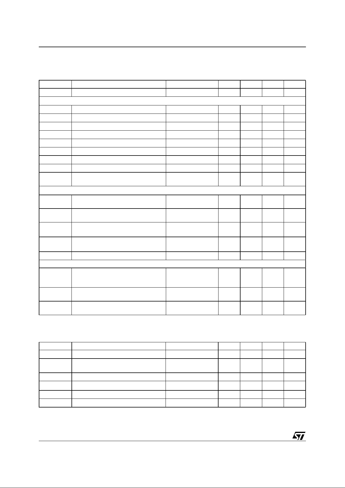
DIM.
mm inch
MIN. TYP. MAX. MIN. TYP. MAX.
A 3.60 0.141
a1 0.10 0.30 0.004 0.012
a2 3.30 0.130
a3 0 0.10 0 0.004
b 0.22 0.38 0.008 0.015
c 0.23 0.32 0.009 0.012
D (1) 15.80 16.00 0.622 0.630
D1 9.40 9.80 0.370 0.385
E 13.90 14.50 0.547 0.570
e 0.65 0.0256
e3 11.05 0.435
E1 (1) 10.90 11.10 0.429 0.437
E2 2.90 0.114
E3 5.80 6.20 0.228 0.244
E4 2.90 3.20 0.114 0.126
G 0 0.10 0 0.004
H 15.50 15.90 0.610 0.626
h 1.10 0.043
L 0.80 1.10 0.031 0.043
N10°(max.)
S8°(max.)
(1): "D" and "E1" do not include mold flash or protrusions
- Mold flash or protrusions shall not exceed 0.15mm (0.006 inch)
- Critical dimensions are "a3", "E" and "G".
PowerSO36
e
a2
A
E
a1
PSO36MEC
DETAIL A
D
118
1936
E1
E2
h x 45˚
DETAIL A
lead
slug
a3
S
Gage Plane
0.35
L
DETAIL B
DETAIL B
(COPLANARITY)
GC
- C -
SEATING PLANE
e3
c
NN
⊕
M
0.12 AB
b
B
A
H
E3
D1
BOTTOM VIEW
OUTLINE AND
MECHANICAL DATA

Information furnished is believed to be accurate and reliable. However, STMicroelectronics assumes no responsibility for the consequences
of use of such information nor for any infringement of patents or other rights of third parties which may result from its use. No license is granted
by implic ation or oth erwise unde r any patent or patent r i ghts of STMi croelectronics. Speci fications mentioned in this publication are subj ect
to change without notice. This publication supersedes and replaces all information previously supplied. STMicroelectronics products are not
authorized for use as crit i cal components in life suppo rt devices or sy st em s without express written approval of STM i croelectronics.
The ST logo is a registered trademark of STMicroelectronics
© 2002 STMic roelectronic s - All Rights Reserved
STMicroelectronics GROUP OF COMPANIES
Australi a - Brazil - China - Finland - France - Germany - Hong Ko ng - India - Italy - Japan - Malaysia - Mal ta - Morocco - Singapore - Spai n
- Sweden - Sw itzerland - United Kingdom - U.S.A.
http://www.s t. com
21/21
L9352
 Loading...