

QUAD INTELLIGENT POWER LOW SIDE SWITCH
■
Quad power l ow side driver wi t h 2 x 5A and
2 x 3A output current capability
■
Low R
= 25°C
@ T
j
■
Internal output clamping structures with
V
= 50V for fast inductive load current
FB
typically 200mΩ and 300m
DSON
recirculation
■
Limited output voltage slew rate for low EMI
■
Protected µP compatible enable and input
■
Wide operati ng supply voltage ra nge 4.5 V to 32V
■
Real time diagnostic functions:
– Output shorted to GND
– Output shorted to V
SS
– Open load detection in ON and OFF condition
– Load bypass detection
– Overtemperature detection
■
Device protection functions:
– Overload disable
– Selective thermal shutdown
■
Signal- and Power-Ground-loss shutdown
Ω
L9349
PowerSO20 BARE DIE
ORDERING NUMB ERS :
L9349 L9349DIE1
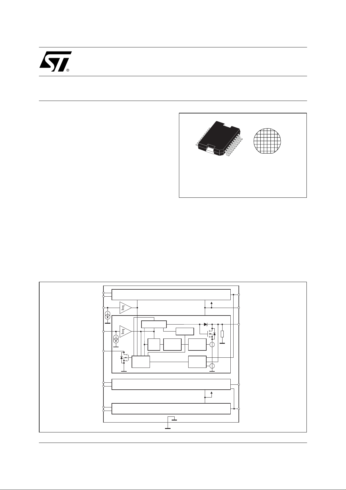
DESCRIPTION
The L9349 is a monolithic integrated quad low side
driver realized in an advanced M ultipowerBCD mixed
technology. The device is intended to drive valves in
automotive environment.
The inputs are µP compatible. Particular care has
been taken to protect the device against failures, to
avoid electromagnetic interferences and to offer extensive real time diagnostic.
BLOCK DIAGRAM
September 2002
IN1
D1
EN
IN4
D4
IN2
D2
IN3
D3
00AT0025
Output Control
Diagnostic
Control
R
QS
Channel 1
Delay
Time
Channel 4
Channel 2
Channel 3
GND
Overtemp
Overload
Openload
52V
OUT1
VS
OUT4
R
IO
OUT2
OUT3
1/12
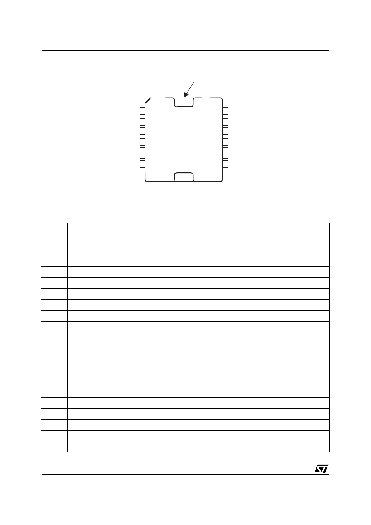
L9349
PIN CONNECTION
Heat sink connected
to pins 1, 10, 11, 20
PGND 1
OUT1 2
D1
3
IN4 4
VS 5
NC
6
IN3 7
D2 8
OUT2
9
PGND 10
00AT0026
PIN DESCRIPTION
N° Pin Function
1 PGND Power Ground
2 Out1 Output 1 (5A)
3 D1 Diagnostic 1
4 IN4 Input 4
5 VS Supply Voltage
20 PGND
OUT4
19
D418
IN117
EN
16
GND15
IN214
D3
13
OUT312
PGND11
6 NC Not Connected
7 IN3 Input 3
8 D2 Diagnostic 2
9 Out2 Output 2 (5A)
10 PGND Power Ground
11 PGND Power Ground
12 Out3 Output 3 (3A)
13 D3 Diagnostic 3
14 IN2 Input 2
15 GND Signal Ground
16 EN Common Enable
17 IN1 Input 1
18 D4 Diagnostic 4
19 Out4 Output 4 (3A)
20 PGND Power Ground
2/12
THERMAL DATA
Symbol Parameter Value Unit
L9349
R
Th j-case
Thermal resistance junction to case 3 °C/W
ABSOLUTE MAXIMUM RATINGSI
Symbol Parameter Conditions Value Unit
V
V
SP
dVS/dt
V
IN, EN
V
V
ODC
I
O1, 2
I
O3, 4
I
OR1, 2
I
OR3, 4
E
O1, 2
E
O3, 4
V
∆
GND
T
jEO
T
T
stg
T
jDIS
ESD Electrostatical Discharging MIL883C +-2 kV
ESD OUT1 - 4 vs. Common-GND
DC Supply Voltage -0.3 to 32 V
S
Supply Voltage Pulse (duration <200ms) -0.3 to 45 V
Supply Voltage Slope 10
Input Voltage
Diagnostic DC Output Voltage
D
I
I
10mA
50mA
-1.5 to 6 V
-0.3 to 16 V
DC Output Voltage -0.3 to 45 V
DC Output Current Out 1, 2 5 A
DC Output Current Out 3, 4 3 A
Reverse Output Current -5 A
Reverse Output Current -3 A
Switch-off Energy for Inductive Loads
tEO = 250µs,
1)
50 mJ
T = 5ms 30 mJ
GND Potential Difference Tj = -40 to 150°C ±0.3 V
Junction Temperature During Switch-off
Junction Temperature -40 to T
j
Σt ≤
Σt ≤
30 min
15 min
175 °C
190 °C
jDIS
Storage Temperature -55 to 150 °C
Thermal Disable Junction Temp. Threshold 180 to 210 °C
+-4 kV
(PGNDs + GND)
V/µs
°C
1) tEO is the clamping time (see F i gure 1)
Electrical Characteristcs (Operating Range)
The electrical characteristics are valid within the below defined operating range, unless otherwise specified.
Symbol Parameter Test Condition Min. Typ. Max. Unit
V
T
T
1) Parameters guaranteed by corre l ation
Board Supply Voltage 4.5 12 32 V
S
Junction Temperature -40 150 °C
j1
Junction Temperature
j2
15min 1) over life time
Σt ≤
150 T
jDIS
°C
3/12

L9349
g
ELECTRICAL CHARACTERISTICS
(V
= 4.5 to 32V; -40°C ≤ Tj1 ≤ 150°C < Tj2 ≤ T
S
jDIS
Symbol Parameter Test Conditions
Supply
I
VS OFF
I
VS ON
DC Supply Current Off EN = 1.0V 5 10 mA
DC Supply Current On
VS ≤ 14V; VIN, VEN = 2V
Diagnostic Outputs D1 - D4
V
Diagnostic Output Low
DL
≤ 3mA
I
D
Voltage
I
DLE
Diagnostic Output
Leakage Current
VD = 14V
1)
Outputs Out 1 - Out 4
R
DSON 1, 2
R
DSON 3, 4
Output On Resistance Tj = 25°C
T
= 150°C
j
VS > 9.5V I
Tj = 25°C
O1,2
Tj = 150°C
VS > 9.5V
I
= 1.3A
O3,4
, unless other-wise specified.)
Values T
Min. Typ. Max. Min. Max.
8mA
0.65 1.0 1.5 V
0.1 2 20
200 300
= 2A
300 450
j1
Values T
j2
Unit
A
µ
m
Ω
500
m
Ω
750
V
Z
R
O
V
OUV 1-4
V
OUV hys 1-
4
∆
V
OUV 1-4,
2-3, 4-1, 3-2
Z-diode clamping
e
volta
Output pull down
resistor
Open Load Voltage
I
≥ 200mA
OCL
VS > 9.5V
EN = 0V
VIN = 1V 0.525 x
Threshold
Hysteresis 0.003 x
Open Load Difference
Voltage Thres hold
V
IN1,4/2,3
= 1V VS ≤ 16V
VOc Š 4.5V
= output voltage of
V
OC
45 60 V
10 40 50
V
V
OC
1.0V
0.55 x
S
V
V
-
V
OC
1.25V
0.575 x
S
S
V
S
V
-
OC
-
1.5V
other channel
V
∆
OUV hys
1-4, 2-3,
4-1, 3-2
I
OUC 1, 2, 3,
4
I
OOC 1, 2
I
OOC 3, 4
Open Load Hysteresis 40 mV
Open Load Current
Threshold
Over Load Current
Threshold
VEN=VIN=2V;
VS=6.5 - 16V
> 6.5V;
V
S
V
= 32V
OUT
160 320 480 mA
510 A
36 A
TSDThermal Shut Down 180 195 210 °C
k
Ω
V
V
V
T
SD-hys
Thermal Shut Down
20 °C
hysteresis
4/12
 Loading...