

■
SUPPLY VOLTAGE RANG E: 4. 8 TO 18V
■
OUTPUT VOLTAGE UP TO 40V
■
OUTPUT VOLTAGE CLAMP DURING
RECIRCULATION OF INDUCTIVE LOADS
■
OUTPUT CURRENT CAPABIL ITY 2 X 5A AND
2 X 3A
■
LOW POWER DISSIPATION DURING
RECIRCULATION OF INDUCTIVE LOADS BY
INTEGRATED FREE WHEELING DIODES
(3A-DRIVER S ONLY)
■
LOW ON-RESISTANCE 2 X 0.2Ω , 2 X 0.35Ω (TYP.)
■
OUTPUT SHORT CIRCUIT CURRENT
PROTECTION
■
REAL TIME DIAGNOSTIC FUNCTIONS
■
OVERTEMPERATURE SHUTDOWN
■
SIGNAL- AND POWER-GROUND-LOSS
SHUTDOWN
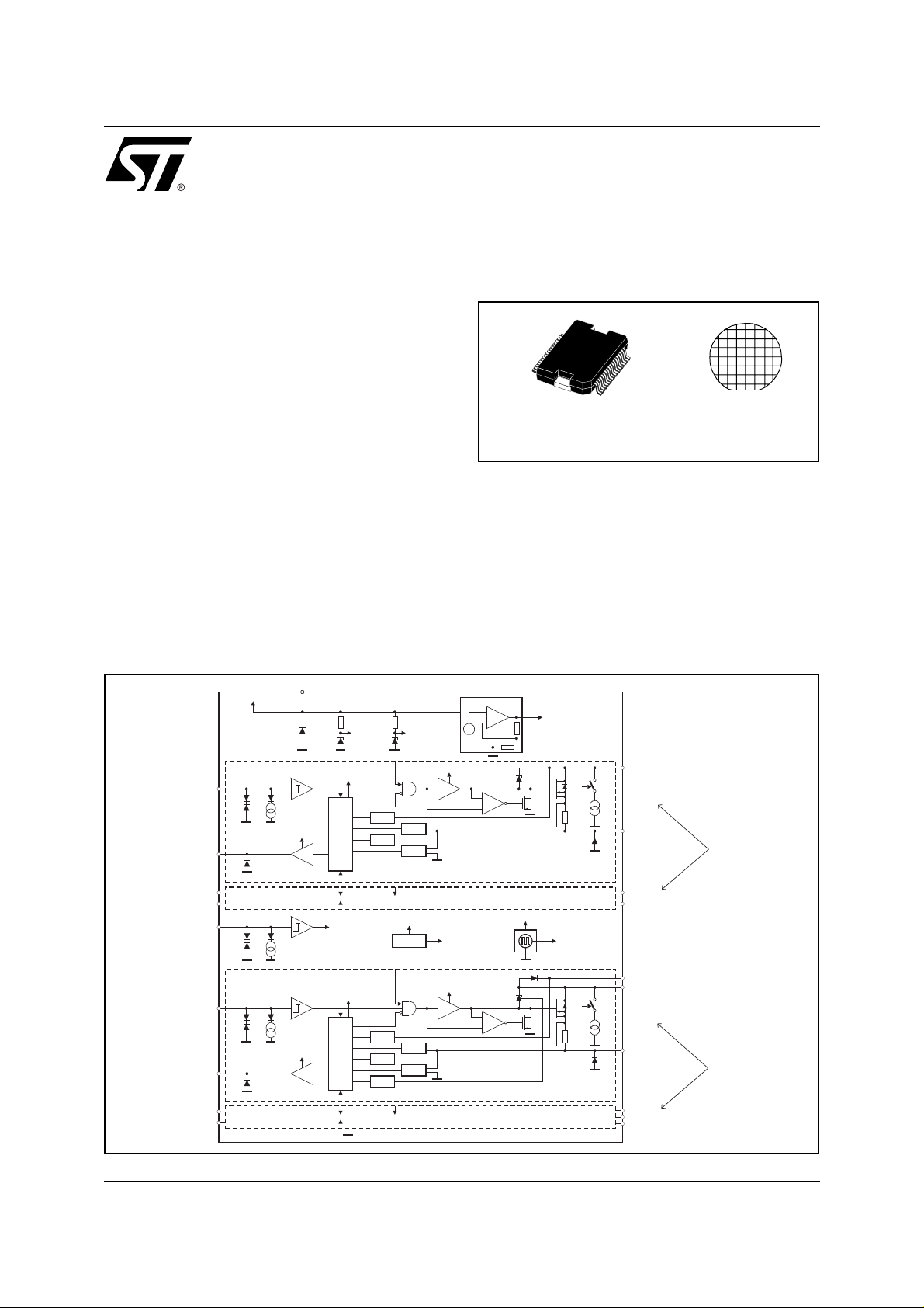
L9348
QUAD LOW SIDE DRIVER
PowerSO-36 BARE DIE
ORDERING NUMB ERS :
L9348 L9348-DIE1
■
3.3V CMOS COMPATIBLE INPUTS AND
STATUS
DESCRIPTION
The L9348 is a monolithic integrated quad low side
driver realized in advanced Multipower-BCD technology. It is intended to drive inductive loads (relays,
electromagnetic valves) in automotive and industrial
applications.
Figure 1. Block Diagram
V
S
IN1
ST1
IN2
ST2
ENA
IN3
ST3
IN4
ST4
99AT0073
March 2002
VS
C 166kHz
V
DD
V
REG
Diagnostic
PWRES
C 166kHz EN
PWRES
EN
C 166kHz
V
DD
V
REG
Diagnostic
PWRES
C 166kHz EN
PWRES
GND
Voltage Regulator
+
–
=
V
S
≥
1
PWRES C 166kHz
V
S
≥
1
TSD
TSD
V
CC
EN
OL
SCP
GL
V
DD
PWRES
EN
OL
SCP
GL
FB
V
DD
FAIL
FAIL
VREG
Q1
EN
PGND1
5A - DRIVER
CHANNEL1
CHANNEL2
V
S
EN
CHANNEL3
CHANNEL4
Q2
PGND2
D3
Q3
PGND3
D4
Q4
PGND4
3A - DRIVER
1/13
L9348
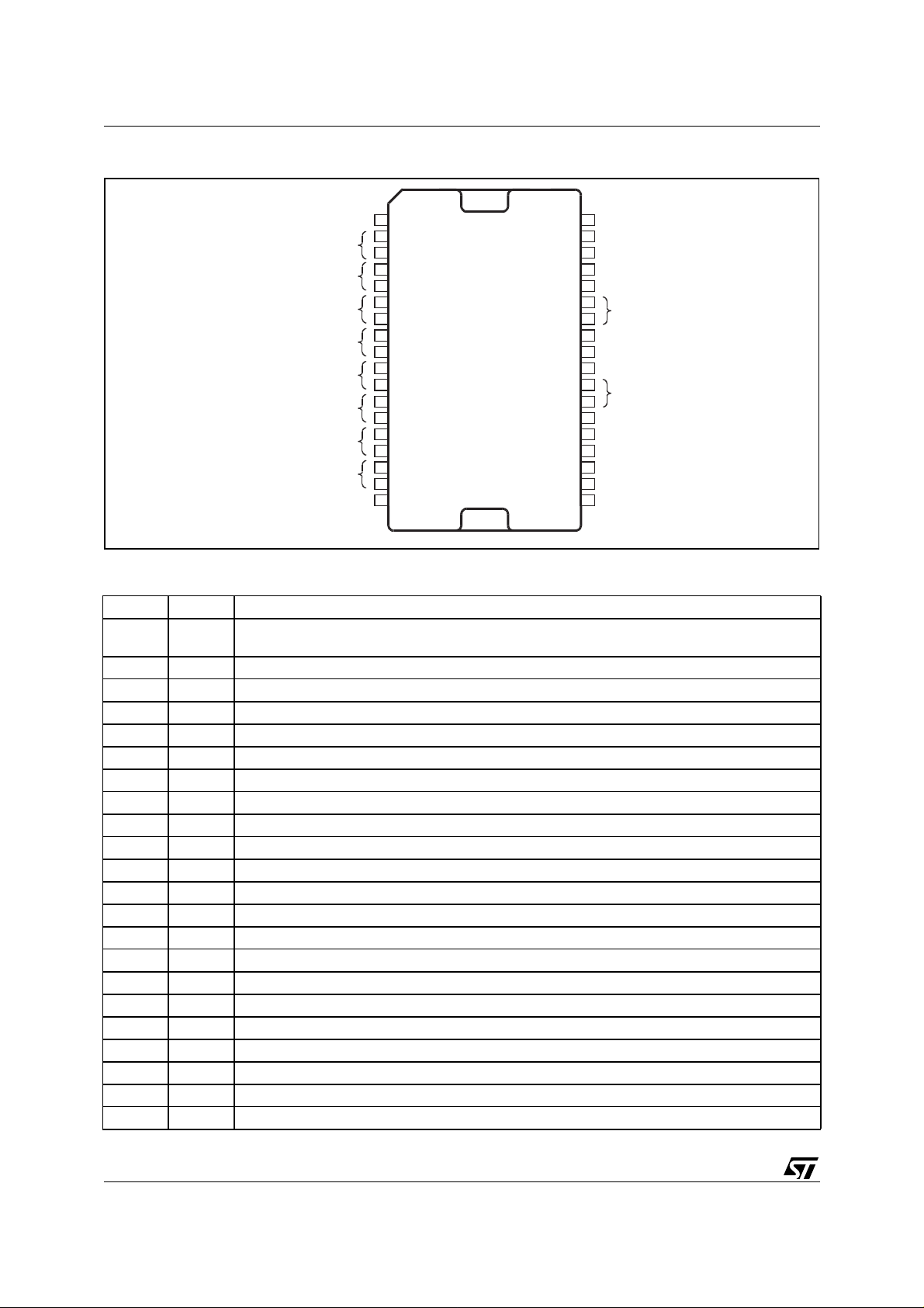
Figure 2. Pin Connection
N.C.
PGND3
Q3
D3
Q1
Q2
D4
Q4
PGND4
N.C.
99AT0074
1
2
3
4
5
6
7
8
9
10
11
12
13
14
15
16
17
18
Table 1. Pin Description
N° Pin Function
1, 18,
19, 36
2, 3 PGND3 Power Ground Channel 3
4, 5 Q3 Power Output Channel 3 (3A switch)
6, 7 D3 Recircula tion Diode Chan nel 3
8, 9 Q1 Power Output Channel 1 (5A switch)
10, 11 Q2 Power Output Channel 2 (5A switch)
12, 13 D4 Recircula tion Diode Chan nel 4
14, 15 Q4 Power Output Channel 4 (3A switch)
16, 17 PGND4 Power Ground Channel 4
20 ST4 Status Output Channel 4
21 IN2 Control Input Channel 2
22 IN4 Control Input Channel 4
23 ST2 Status Output Channel 2
24 ENA Enable
25, 26 PGND2 Power Ground Channel 2
27 GND Signal Ground
28 VS Supply Voltage
29 N.C. Not Connected
30, 31 PGND1 Power Output Channel 3
32 ST1 Status Output Channel 1
33 IN3 Control Input Channel 3
34 IN1 Control Input Channel 1
N.C. (GND)
36
35
34
33
32
31
30
29
28
27
26
25
24
23
22
21
20
19
N.C.
ST3
IN1
IN3
ST1
PGND1
N.C.
VS
GND
PGND2
ENA
ST2
IN4
IN2
ST4
N.C.
2/13
Table 2. Thermal Data
Symbol Parameter Test Conditions
T
Junction temperature -40 150 °C
j
L9348
Values
Unit
Min. Typ. Max.
T
T
R
th j-case
Junction temperature during
jc
clamping (life time)
Storage temperature -55 150 °C
stg
t = 30min
Σ
t = 15min
Σ
Thermal resistance junction to
175
190
2 °C/W
°C
°C
case
Table 3. Absolute Maximum Ratings
The absolute maximum ratings are the limiting values for this device. Damage may occur if this device is
subjected to conditions which are beyond these values
Symbol Parameter Test Conditions Value Unit
Voltages
V
S
V
, V
Q
D
, V
V
IN
EN
V
ST
V
DRmax
Currents
I
Q 1/2
I
Q 3/4
I
ST
E
Q1/2
I
FDmax
ESD Protection
Supply and Signal pins versus GND ±2kV
Output pins (Q
Supply voltage range -0.3 to 40 V
max. static Output voltage 40 V
Input voltage range
|II | < 10mA -1.5 to 6 V
(IN1 to IN4, EN)
Status output voltage range |II | < 1mA -0.3 to 6 V
max. Reverse breakdown
= 100 µA
I
R
voltage free wheeling diodes
D3, D4
Output current at reversal
supply for Q1, Q2
Output current at reversal
supply for Q3, Q4
Status output current range -1 to 1 mA
max. Discharging energy for
inductive loads per channel
Q1, Q2
max. load current free
= 25°C 50 mJ
T
j
T
= 150°C 30 mJ
j
t < 5ms 3 A
wheeling diodes
, DX) versus common ground (=short of
X
.
55 V
-4 A
-2 A
±4kV
SGND with all PGND)
Note: Human Body Model according to MIL883C. The device withstands ST1 class level.
Table 4. Operating Range
.
Symbol Parameter Test Conditions
V
S
T
Supply voltage 4.8 18 V
Junction temperature -40 150 °C
j
Values
Min. Typ. Max.
Unit
3/13
L9348
Table 5. Electrical Characteristcs
The electrical characteristics are valid within the operating range
Symbol Parameter Test Condition Min. Typ. Max. Unit
Power Supply
I
Supply current V
S
I
Quiescent current (outputs OFF) V
Q
IN1...IN4, ENA
= L 6 mA
ENA
= H 8 mA
(Table 4)
, unless otherwise specified
I
D3/4
Quiescent current at pins D3/4
Diagnostic Functions
V
QU1 to 4
Output open load voltage
threshold
I
QU1 to 4
Output open load current
threshold
I
QO1/2
I
QO3/4
Overload current threshold Q 1, 2
Overload current threshold Q 3, 4
TthOvertemperature shutdown
threshold
V
V
T
thPGL
thSGL
Overtemperature hysteresis 10 °C
hy
Power-GND-loss threshold 1.5 2.5 3.5 V
Signal-GND -loss thresh old 150 330 510 mV
Power Outputs (Q1 to Q4)
R
DSON1/2
Static drain-source ON-resistance
Q1, Q2
≤ 18V;
V
D3/4
V
= L
IN3/4
≥ 6.5V
V
S
VEN = X; VIN = L
≥ 6.5V
V
S
VEN = H; VIN = H
≥ 6.5V
V
S
≥ 6.5V
V
S
2)
= 1A; VS ≥ 9.5V
I
Q
Tj = 25°C
Tj = 125°C
3)
10 400
0.3 0.33 0.36 x V
A
µ
S
50 140 mA
57.59 A
358A
175 210 °C
0.2
0.5
Ω
Ω
R
DSON3,4
V
Z
V
C
I
PD
4/13
Static drain-source ON-resistance
Q3, Q4
Z-diode clamping voltage
= threshold of flyback detection
Q3/4
Clamping voltage
Output pull down current V
Tj = 150°C
= 1A; VS ≥ 9.5V
I
Q
T
= 25°C
j
T
= 125°C
j
T
= 150°C
j
≥ 100mA,
I
Q
pos. supply V
≥ 100mA,
I
Q
neg. supply V
ENA
4)
0.35 Ω
3)
4)
45 60 V
D3/4
410V
D3/4
= H, VIN = L 10 20 50
0.5
0.75 Ω
0.75 Ω
µ
Ω
A
 Loading...