

INTELLIGENT QUAD (2X5A/2X2.5A) LOW-SIDE SWITCH
■
Quad low-side switch
■
2 x 5A designed as conventional switch
■
2 x 2.5A designed as switched current-regulator
■
Low ON-resistance 2 x 0.2Ω, 2 x 0.35Ω (typ.)
■
Power SO-36 - package with integrated
cooling area
■
Integrated free-wheeling and clamping Z-diodes
■
Output slope control
■
Short circuit protection
■
Selective overtemperature shutdown
■
Open load detection
■
Ground and supply loss detection
■
External clock control
■
Recirculation control
■
Regulator drift detection
■
Regulator error control
■
Regulator resolution 5mA
■
Status monitoring
■
Status push-pull stages
■
Electrostatic discharge (ESD) protection
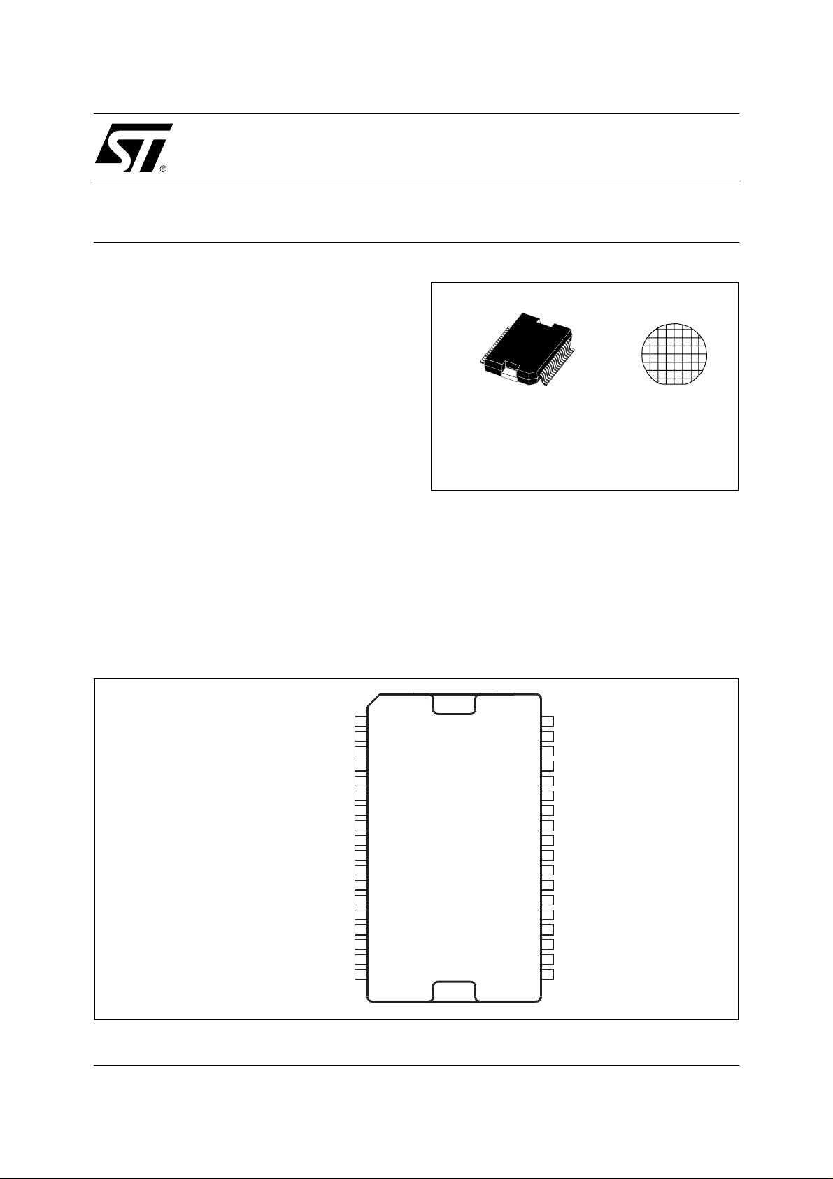
L9347
PowerSO-36 BARE DIE
ORDERING NUMB ERS :
L9347PD L9347DIE1
DESCRIPTION
The L9347 is an integrated quad low-side power
switch to drive inductive loads like valves used in
ABS systems. Two of the four channels are current
regulators with current range from 250mA to 2.25A
and an accuracy of 10%.
All channels are protected against fail functions.
They are monitored by a status output.
Figure 1. Pin Connection
99AT0060
June 2002
GND 1
PGND3
PGND3
Q3
Q3
D3
D3
Q1
Q1
Q2
Q2
D4
D4
Q4
Q4
PGND4
PGND4
N.C.
2
3
4
5
6
7
8
9
10
11
12
13
14
15
16
17
18
36
35
34
33
32
31
30
29
28
27
26
25
24
23
22
21
20
19
CLK
ST3
IN1
IN3
ST1
PGND1
PGND1
VS
PGND2
PGND2
TEST
EN
ST2
IN4
IN2
ST4
VDD
VCC
1/21
L9347
Figure 2. Block Diagram
EN
VS VCC VDD
Internal Supply
CLK
IN1
ST1
IN4
ST4
IN2
Overtemperature
Channel 4
Overtemperature
Channel 3
LOGIC
LOGIC
&
DA
LOGIC
Overtemperature
Channel 1
Open Load
Overload
GND-det.
Open Load
Overload
GND-det.
Overtemperature
Channel 2
Open Load
Overload
Q1
IPD
D4
Q4
IPD
Q2
2/21
ST2
IN3
ST3
TEST
99AT0059
drift-det.
LOGIC
&
DA
GND-det.
Open Load
Overload
GND-det.
IPD
D3
Q3
IPD
GND
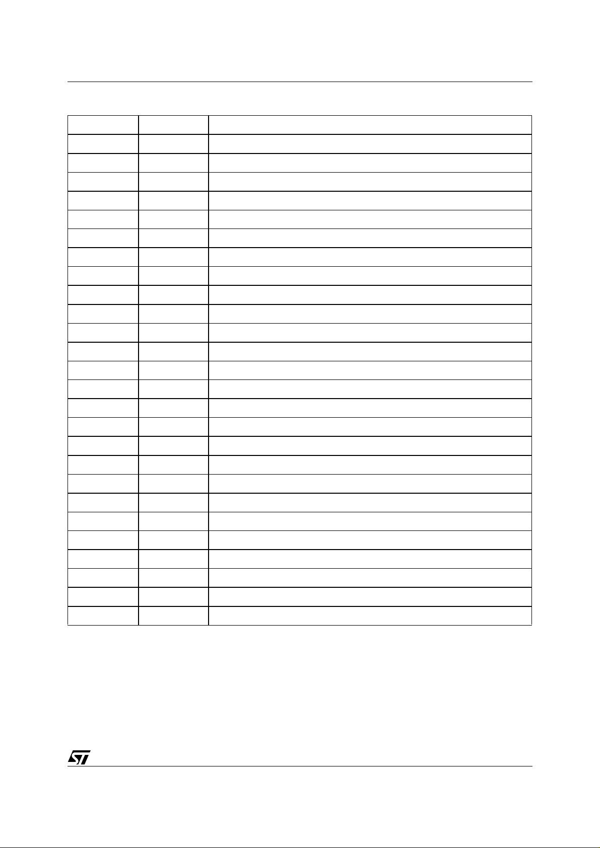
PIN DESCRIPTION
N° Pin Function
1 GND Logic Ground
2, 3 PGND 3 Power Ground Channel 3
4, 5 Q 3 Power Output Channel 3
6, 7 D 3 Free-Wheeling Diode Channel 3
8, 9 Q 1 Power Output Channel 1
10, 11 Q 2 Power Output Channel 2
12, 13 D 4 Free-Wheeling Diode Channel 4
14, 15 Q 4 Power Output Channel 4
16, 17 PGND 4 Power Ground Channel 4
18 NC Not Connected
19 VCC 5V Supply
20 VDD 5V Supply
L9347
21 ST 4 Status Output Channel 4
22 IN 2 Control Input Channel 2
23 IN 4 Control Input Channel 4
24 ST 2 Status Output Channel 2
25 EN Enable Input for all four Channels
26 TEST Enable Input for Drift detection
27, 28 PGND 2 Power Ground Channel 2
29 VS Supply Voltage
30, 31 PGND 1 Power Ground Channel 1
32 ST 1 Status Output Channel 1
33 IN 3 Control Input Channel 3
34 IN 1 Control Input Channel 1
35 ST 3 Status Output Channel 3
36 CLK Clock Input
3/21
L9347
ABSOLUTE MAXIMUM RATINGS
The absolute maximum ratings are the limiting values for this device. Damage may occur if this device is subjected to conditions which are beyond these values.
Symbol Parameter Test Conditions Min Typ Max Unit
E
Q
Voltages
V
S
V
, V
CC
V
Q
V
Q
V
, V
IN
V
CLK
V
ST
V
D
V
DRmax
Currents
I
Q1/2
I
Q3/4
I
Q1/2
I
PGND1/2
I
Q3/4
I
PGND3/4
I
ST
ESD Protection
ESD Elec trost atical Disch argin g MIL883C ±2kV
ESD Output Pins (Qx, Dx) vs. Common GND
Switch off energy for inductive loads 50 mJ
Supply voltage -0.3 40 V
Supply voltage -0.3 6 V
DD
Output voltage static 40 V
Output voltage during clamping t < 1ms 60 V
Input voltage IN1 to IN4, EN II < |10|mA -1.5 6 V
EN
Input Voltage CLK -1.5 6 V
Output voltage status -0.3 6 V
Recirculation circuits D3, D4 40 V
max. reverse breakdown voltage of free
wheeling diodes D3, D4
Output current for Q1 and Q2 >5
Output current for Q3 and Q4 >3
,
Output current at reversal supply for Q1
-4 A
and Q2
,
Output current at reversal supply for
-2 A
Q3 and Q4
Output current status pin -5 5 mA
±4kV
(PGND1-4 + GND)
55 V
internal
limited
internal
limited
A
A
THERMAL DATA
Symbol Parameter Test Conditions Min Typ Max Unit
T
j
T
jc
Junction temperature T
Junction temperature during clamping
(life time)
T
stg
T
th
T
hy
R
thJC
(1) This parameter will not be tested but assured by design.
Storage temperature T
Overtemperature shutdown threshold
Overtemperature shutdown hysteresis
Thermal resistance junction to case R
4/21
j
t = 30min
Σ
t = 15min
Σ
stg
(1)
(1)
thJC
-40 150 °C
175
190
-55 150 °C
175 200 °C
10 °C
2 K/W
°C
L9347
OPERATING RANGE
Symbol Parameter Test Conditions Min. Typ. Max. Unit
V
, V
V
CC
dV
S
V
V
V
ST
I
ST
T
T
jc
.
ELECTRICAL CHARACTERISTCS
(Vs = 4.8 to 18V; T
Symbol Parameter Test Condition Min. Typ. Max. Unit
Supply voltage 4.8 18 V
S
Supply voltage 4.5 5.5 V
DD
/dt Supply voltage transient time -1 1
Output voltage static -0.3 40 V
Q
Output voltage induced by inductive switching Voltage will be
Q
limited by internal
Z-diode clamping
Output voltage status -0.3 6 V
Output current status -1 1 mA
Junction temperature -40 150 °C
j
Junction temperature during clamping
= 30min
Σ
= 15min
Σ
:
= -40 to 150°C unless otherwise specified)
j
60 V
175
190
V/
°C
s
µ
Power Supply
I
SON
I
SOFF
Supply current
Quiescent current
I
Supply current VCC (analog supply) VCC =5V 5 mA
cc
I
Supply current VDD (digital supply) VDD =5V f
dd
I
Supply current VDD (digital supply) VDD =5V f
dd
General Diagnostic Functions
V
V
thGND
V
thPGL
f
CLK,min
DC
DC
high
Open load voltage
QU
Signal-GND-loss threshold VCC= 5V 0.1 1 V
Power-GND-loss thresh old VCC = 5V 1.5 2.5 3.5 V
Clock frequency error 10 100 kHz
Clock duty cycle error detection low f
CLKe_l
ow
Clock duty cycle error detection high f
CLKe_
V
S
≤ 18V
5mA
(outputs ON)
V
S
≤ 18V
5mA
(outputs OFF)
=0Hz 5 uA
CLK
=250kHz 5 mA
CLK
V
S
≥ 6.5V
0.3 0.33 0.36 x V
(outputs OFF)
= 250 kHz 33,3 45 %
CLK
= 250 kHz 55 66,6 %
CLK
Q
VS
Supply detection VCC = VDD = 5V 2 4.5 V
loss
Additional Diagnostic Functions channel 1 and channel 2 (non regulated channels)
I
QU1,2
I
QO1,2
Open-load current channel 1, 2
Over-load current channel 1, 2
V
S
V
S
≥ 6.5V
≥ 6.5V
50 140 mA
57.59 A
5/21
L9347
ELECTRICAL CHARACTERISTCS
:
(continued)
(Vs = 4.8 to 18V; Tj = -40 to 150°C unless otherwise specified)
Symbol Parameter Test Condition Min. Typ. Max. Unit
Additional Diagnostic Functions channel 3 and channel 4 (regulated channels)
DC
I
QO3,4
V
PWM
Digital Inputs (IN1 to IN4, ENA, CLK, TEST). The valid PWM-Ratio for IN3/IN4 is 10% to 90%
V
V
Digital Outputs (ST1 to ST4)
V
Output duty cycle range filtered with 10ms 10 90 %
OUT
Overload current
V
S
≥ 6.5V
2.5 5 8 A
channel 3,4
Recirculation error shutdown
rerr
Iout > 50mA 45 50 60 V
threshold (open D3/D4)
Output PWM ratio during drift
dOU
T
comparison
Input low voltage -0.3 1 V
V
IL
Input high voltage 2 6 V
IH
IHy
Input voltage hysteresis
I
Input pull down current
I
STL
Status output voltage in low state
(1)
(2)
V
= V
IN3
V
V
IN4
= H
TEST
= 5V, VS ≥ 6.5V
IN
IST ≤ 40µA
= PWM
IN
-14.3 +14.3 %
20 500 mV
82040
0 0.4 V
A
µ
V
STH
Status output voltage in high state
R
DIAGLROUT
R
DIAGHROUT
+ R
+ R
DSON
DSON
Power Outputs (Q1 to Q4)
R
DSON1,2
Static drain-source ON-resistance
Q1 and Q2
(non-reg. channels)
R
DSON3,4
Static drain-source ON-resistance
Q3 and Q4
(reg. channels)
V
F_250mA
Forward voltage of free wheeling path
D3, D4 @250mA
V
F_2.25A
Forward voltage of free wheeling path
D3, D4 @2.25A
R
Sense resistor = (V
sens
2A
2)
IST ≥ -40µA
I
≥ -120µA
ST
2.5 3.45 V
23.45V
in low state 0.3 0.64 1.5
in high state 1.5 3.2 7.0
= 1A; VS ≥ 9.5V
I
Q
0.2
0.5
0.5
0.35
0.75
0.75
1
F_2.25A-VF_250mA
= 25°C
T
j
Tj = 125°C
Tj = 150°C
= 1A; VS ≥ 9.5V
I
Q
= 25°C
T
j
= 125°C
T
j
Tj = 150°C
I
D3/4
I
D3/4
)/
(3)
(4)
3)
4)
= -250mA 0.5 1.5 V
= -2.25A 2.0 4.5 V
k
Ω
k
Ω
Ω
Ω
Ω
Ω
Ω
Ω
Ω
6/21
L9347
ELECTRICAL CHARACTERISTCS
:
(continued)
(Vs = 4.8 to 18V; Tj = -40 to 150°C unless otherwise specified)
Symbol Parameter Test Condition Min. Typ. Max. Unit
V
Z-diode clamping voltage
Z
I
Output pull down current VEN = H, VIN = L 10 150
PD
I
Output leakage current VEN = L; VQ = 20V 5
Qlk
Timing
t
t
t
OFFREG
t
Output ON delay time
ON
Output OFF delay time channel
OFF
Output OFF delay time regulator
Output rise time
t
r
Output fall time
t
f
t
sf
Short error detection filter time f
t
lf
Long error detection filter time f
Short circuit switch-OFF delay time
SCP
t
Status delay time
D
t
Regulation error status delay time
RE
≥ 100mA
I
Q
= 1A
I
Q
IQ = 1A
(5)
IQ = 1A
= 1A
I
Q
= 250kHz DC = 50%
CLK
= 250kHz DC = 50%
CLK
(5)
(5)
(5)
(reg. channels only)
(5)
(5)
45 60 V
0520
01030
528
0.5 1.5 8
0.5 1.5 8
48
16 32
430
896 1024 us
10 ms
A
µ
A
µ
s
µ
s
µ
s
µ
s
µ
s
µ
s
µ
s
µ
s
µ
t
Dreg
Output off status delay time
(5)
(reg. channels only
528
Reg. Current Accuracy (reg. channels only)
I
Q3/Q4
I
Q3/Q4
I
I
∆
REG
Minimum current DC = 10% 200 250 300 mA
Maximum current DC = 90% 2 2.25 2.5 A
Max. regulation deviation @
DC 10% - 90%
Min. quant. step 5 mA
Q3/Q4
250mA < I
400mA ≤ I
800mA < I
Q3/Q4
Q3/Q4
Q3/Q4
< 400mA
≤ 800mA
< 2.25A
Frequencies
CLK frequency crystal-controlled 250 kHz
Input PWM frequency (reg. channels only) 2 kHz
(1) This parameter will not be tested but assured by design
(2) Short circuit between two digital outputs (one in high the other in low state) will lead to the defined result "LOW"
(3) Measured chip, bond wires not i ncluded
(4) Measured on Power SO-36 devices
(5) Digital filtered with external clock, only functional test
±10
±6
±10
s
µ
%
%
%
7/21
 Loading...