

QUAD INTELLIGENT POWER LOW SIDE SWITCH
QUADPOWERLOWSIDE DRIVERWITH 2x 5A
AND 2 x 3AOUTPUT CURRENTCAPABILITY
DSON
LOW R
@Tj=25°C
INTERNAL OUTPUT CLAMPING STRUCTURES WITH V
TIVELOAD CURRENTRECIRCULATION
LIMITED OUTPUT VOLTAGE SLEW RATE
FOR LOW EMI
PROTECTED µP COMPATIBLE ENABLE
AND INPUT
WIDE OPERATING SUPPLY VOLTAGE
RANGE4.5V TO 32V
REAL TIMEDIAGNOSTICFUNCTIONS:
- OUTPUTSHORTED TO GND
- OUTPUTSHORTED TO VSS
- OPENLOAD MEASUREDIN ON AND OFF
CONDITION
- LOADBYPASS DETECTION
- OVERTEMPERATURE
DEVICEPROTECTIONFUNCTIONS:
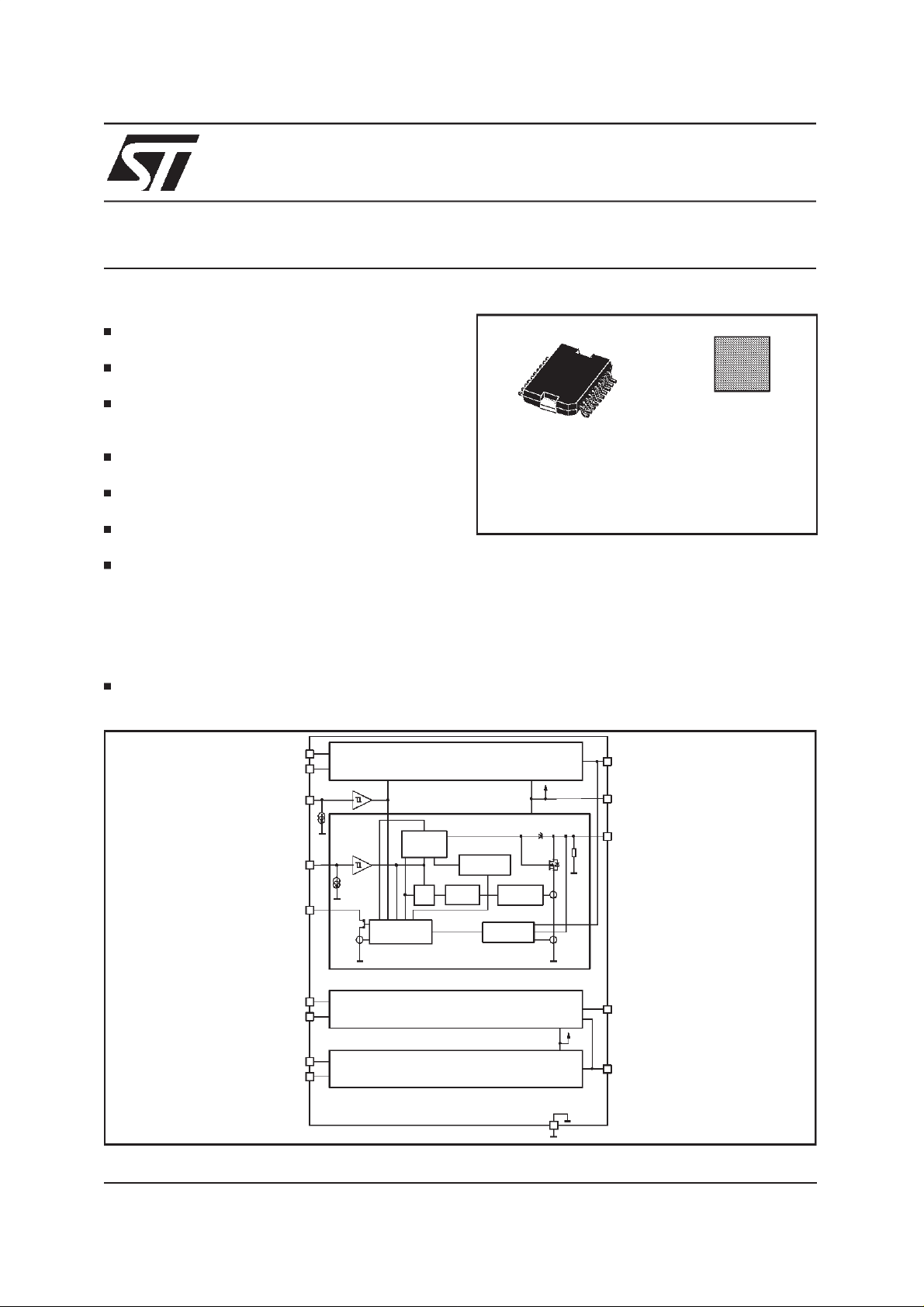
BLOCK DIAGRAM
TYPICALLY200mΩ AND 300mΩ
FB = 50V FOR FAST INDUC-
L9346
Power SO20
ORDERING NUMBERS: L9346PD (power SO20)
L9346DIE (chip)
- OVERLOAD DISABLE
- REVERSESUPPLYVOLTAGE
PROTECTEDVS UPTO-2V
- SELECTIVETHERMAL SHUTDOWN
DESCRIPTION
The L9346 is a monolithic integrated quad low
side driver realized in an advanced Multipow-
Chip
May 2000
IN1
D1
EN
IN4
D4
IN2
D2
IN3
D3
Diagnostic
Control
Output
Control
QS
Channel1
52V
Overtemp
Delay
R
Timer
Channel4
Channel2
Channel3
Overload
Openload
GND
OUT1
VS
OUT4
R
IO
OUT2
OUT3
1/13
L9346
DESCRIPTION
(continued)
erBCD mixed technology. The device is intended
to drive valves in automotiveenvironment.
The inputsare µP compatible. Particularcare has
been taken to protect the device against failures,
to avoid electromagnetic interferences and to offer extensive realtime diagnostic.
ABSOLUTE MAXIMUM RATINGS
Symbol Parameter Conditions Value Unit
V
S
SP Supply Voltage Pulse (duration <200ms) -2 to 45 V
V
dV
S
dt
V
IN, EN
V
D
ODC DC Output Voltage -0.3 to 45 V
V
O1, 2 DC Output Current Out 1, 2 5 A
I
O3, 4 DC Output Current Out 3, 4 3 A
I
OR1, 2 Reverse Output Current -5 A
I
OR3, 4 Reverse Output Current -3 A
I
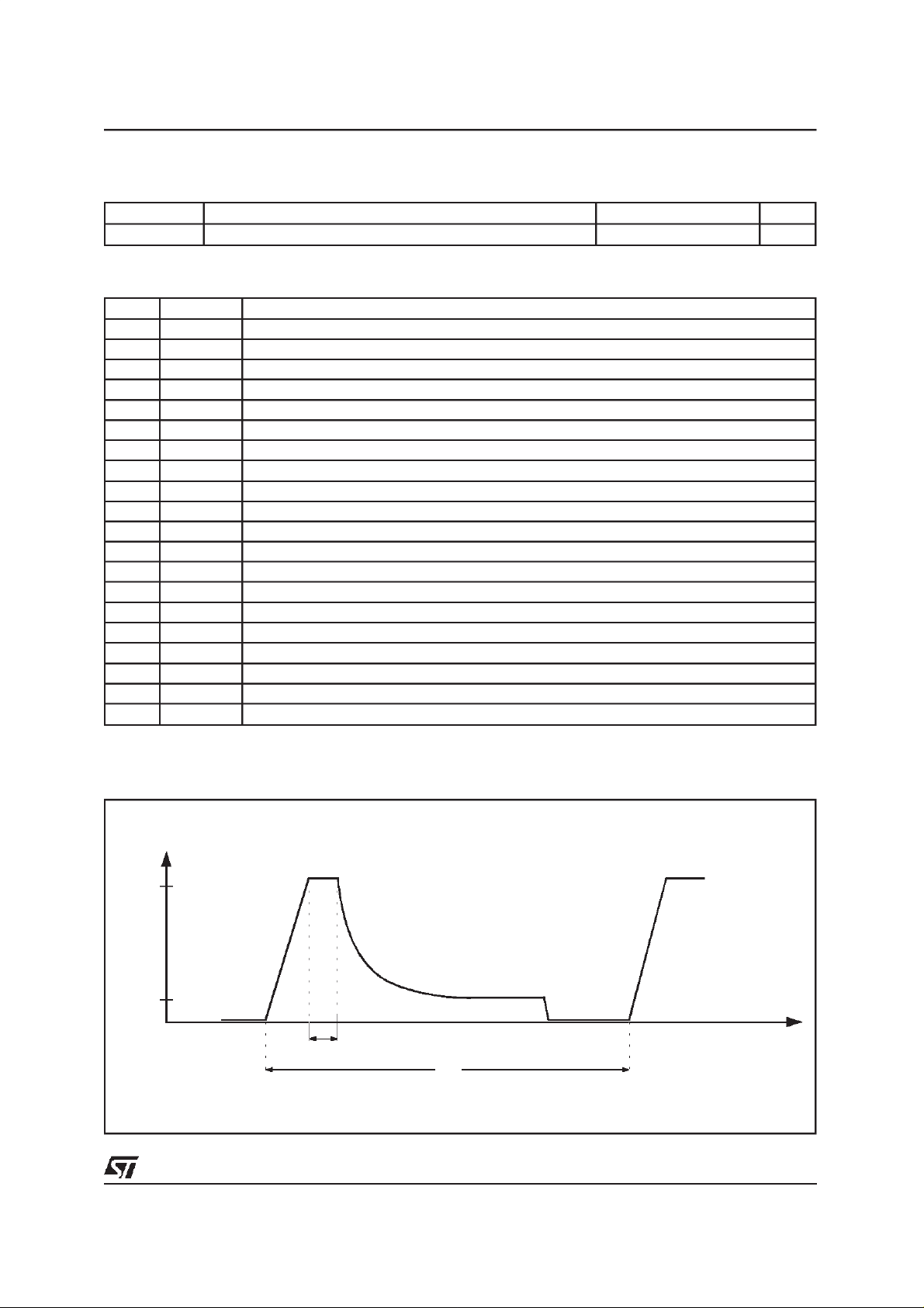
O1,2 Switch-off Energyfor Inductive Loads tEO = 250µs,
E
O3,4 T = 5ms 30 mJ
E
∆V
GND
T
jEO
j Juntion Temperature -40 to TjDIS °C
T
stg Storage Temperature -55 to 150 °C
T
jDIS Thermal DisableJunction Temp. Threshold 180 to 210 °C
T
DC Supply Voltage -2 to 32 V
Supply Voltage Slope 10 V/µs
Input Voltage I 10mA -2 to 16 V
Diagnostic DC Output Voltage I 50mA -0.3 to 16 V
1)
50 mJ
GND Potential Difference Tj= -40 to 150°C ±0.3 V
Juntion Temperature During Switch-off ∑t ≤ 30 min 175 °C
∑t ≤ 15 min 190 °C
The device is ESDprotected, testedaccording to MIL883Cwith ±2KV.
1)
:tEOis theclamping time (seefig.1)
Note
PIN CONNECTION
Heat sink connected to pins 1, 10, 11, 2 0
PGND
OUT1
D1
IN4
VS
NC
IN3
D2
OUT2
PGND
PGND
OUT4
D4
IN1
EN
GND
IN2
D3
OUT3
PGND
2/13
THERMAL DATA
Symbol Parameter Value Unit
R
th j-c
Thermal Resistance junction to case 3 K/W
PIN FUNCTIONS
N. Name Function
1 GND Power Grounded
2 Out 1 Output 1 (5A)
3 D1 Diagnostic 1
4 IN 4 Input 4
5 VS Supply Voltage
6 NC Not Connected
7 IN 3 Input 3
8 D2 Diagnostic 2
9 Out 2 Output 2 (5A)
10 GND Power Ground
11 GND Power Ground
12 Out 3 Output 3 (3A)
13 D3 Diagnostic 3
14 IN 2 Input 2
15 GND Signal Ground
16 EN Common Enable
17 IN 1 Input 1
18 D4 Diagnostic 4
19 Out 4 Output 4 (3A)
20 GND Power Ground
L9346
Figure 1: tEO ClampingTime
V
O1 - 4
V
OC L
V
S
t
t
EO
T
3/13
L9346
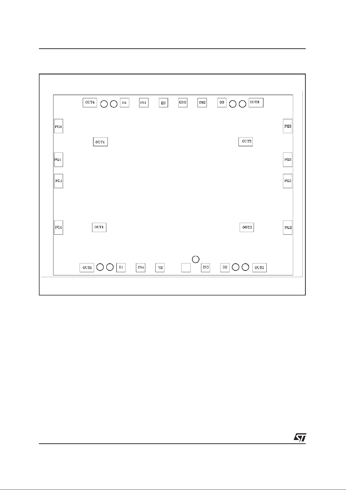
Figure 2: Pad Position
(Chipsize 4.95x 3.88)
ESD
4/13
 Loading...