

L9341
QUAD LOW SIDE DRIVER
AVANCE DATA
DU/DTAND DI/DTCONTROL
PWM CONTROLLEDOUTPUT CURRENT
SHORT CURRENT PROTECTION AND DI-
AGNOSTIC
INTEGRATEDFLYBACKDIODE
UNDERVOLTAGESHUTDOWN
OVERVOLTAGE AND UNDERVOLTAGE DI-
AGNOSTIC
OVERTEMPERATUREDIAGNOSTIC
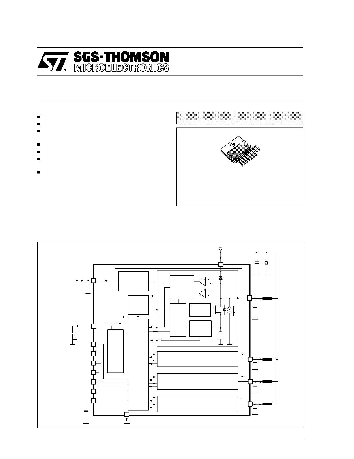
DESCRIPTION
The L9341 is a monolithic integrated circuit realized in Multipower BCD-II mixed technology. The
driver is intended for inductive loads in synchronous PWM applications, especially for valve driv-
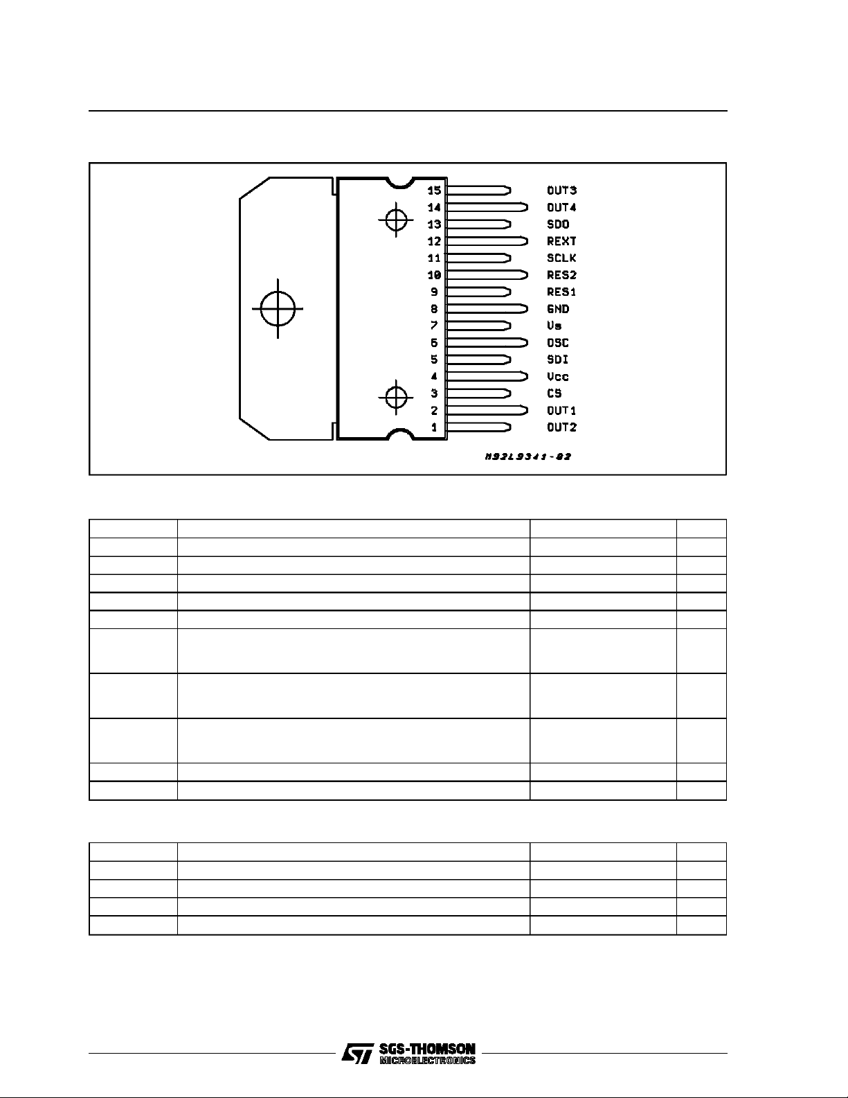
BLOCK & APPLICATION DIAGRAM
VCC
10nF
Vcc
10uF
R
12.4k
4
I
cc
REXT
12
ext
Ω
RES1
9
RES2
10
CS
3
SCLK
11
SDI
5
SDO
13
OSC
6
C
OSC
BIAS
GND
UNDERVOLTAGE
SHUTDOWN
THERMAL
FLAG
SERIAL
INTERFACE
&
PWM
CONTROLL
8
I
GND
MULTIPOWERBCD TECHNOLOGY
Multiwatt 15
ORDERING NUMBERS: L9341V
L9341H
ers. The output voltage and current rise and fall
slopesdu/dt and di/dt are controlled.
V
s
I
CHANNEL 1
DIAGNOSTIC
DRIVER
COMP1
COMP2
di / dt & du / dt
CONTROL
SHORT
CURRENT
PROTECTION
CHANNEL 2
CHANNEL 3
CHANNEL 4
s
VS
7
V
flyth
V
offth
I
220nF
C
BATDBAT
OUT1
2
I
OUT1
10nF
C
outs
O1
OUT2
1
I
OUT2
C
O2
10nF
OUT3
15
I
OUT3
C
O3
10nF
OUT4
14
I
OUT4
C
O4
10nF
March 1994
1/10
This is advanced information on a new productnow in development or undergoing evaluation. Details aresubject to change withoutnotice.
L9341
PIN CONNECTION (Top view)
ABSOLUTE MAXIMUMRATINGS
Symbol Parameter Value Unit
V
CC
V
S
V
spmax
V
st
Vin InputVoltage Range for SDI; SCLK;CS;RES1;RES2 -0.3to V
V
out
I
out
VCCVoltageRange -0.3 to 6 V
VSVoltage Range -0.3 to 24 V
VS Voltage Range for t ≤ 400ms -2 to 40 V
Schaffner Transient Pulses on V
S
see note1 V
+0.3
CC
Output Voltage Range for all Outputs:
Negative
Positive
intern. clamped to V
– 0.3
S
Output Current for all Outputs:
Negative
Positive
–2
+2
for Transient witht < 10ms
Negative
Positive
–5
5
Schaffner Transient Pulses on Output see note2
V
ESD
ESD Voltage Capability (MIL 883 C) 1500 V
THERMAL DATA
Symbol Parameter Value Unit
R
th j-case
R
th j-amb
T
sdh
T
sd
Notes:
1. Schaffner transient specification: DIN 40839 testwaveforms of the following type: 1, 2, 3a, 3b, 5 and 6.
The pulses are applied to the application circuit according to fig. 3.
2. The maximum output current results from theSchaffner pulses specified in note 1.
Thermal Resistance Junction to Case 3 °C/W
Thermal Resistance Junction to Ambient mountedon PC Board 35 °C/W
Thermal Hysteresis 20 °C
Thermal Diagnostic Tj> 150 °C
V
V
A
A
A
A
2/10

L9341
ELECTRICAL CHARACTERISTICS (Unless otherwise specified: 8V ≤ VS≤ 24V; 4.7V ≤ VCC≤ 5.3V; –
40 °C ≤ Tj ≤ 150°C;I
R
=12.4KΩ ± 1%).
ext
≤ 1A(note 3); IO≤ 1.5A;Vsp=VSfor t ≤ 400ms; V
O
OUTP=VOUT
Symbol Parameter Test Condition Min. Typ. Max. Unit
I
ccq
I
sq
V
ccu
V
ccr
VccQuiescent Current All Outputs Off 1 3 mA
VsQuiescent Current All Outputs Off 14 25 mA
VccUndervoltage Threshold See Note 4 3 4 4.7 V
VccRange for RES1 and RES2
3V
Operation
R
on
I
o off
V
outf
I
gndf
I
outr
V
inH
On Resistance Io=1A Tj= 125°C
T
=25°C
j
Off State Output Current Outputs Off
1.4V ≤ V
V
outp=Vsp
≤ V
o
s
= 40V
1
1
Output Voltage During Flyback Io= 1A Output Off
T
=25°C
j
T
= 125°C
j
Current to GND during Flyback
(see note 5)
Io= 1A Output Off
V
= 24V
s
V
= 40V
sp
Reverse Leakage Current Vsp-Vo= 40V 500 µA
High Input Level of SCLK,
0.7*V
cc
SDI, CS, RES1, RES2
V
inL
Low Input Level of SCLK,
– 0.3 0.3*Vcc V
SDI, CS, RES1, RES2
V
REShys
Hysteresis of Reset Inputs
0.3 1 V
RES1, RES2
I
inRESH
I
V
SDOH
V
SDOL
I
SDOZ
PWM
K
V
V
in
f
flyth
offth
Input Current on RES1,RES2 RESi= H; -2V ≤ Vsp≤ 8V
RES
=H;8V≤Vsp≤ 40V
i
–10
5
Input Current on SCLK,SDI,CS – 2V ≤ Vsp ≤ 40V – 10 10 µA
High Level SDO Output Voltage I
Low Level SDO Output Voltage I
SDO TristateHigh-Z Leakage
Current
PWM Duty Cycle 1/16 15/16
duty
= -1mA -2V≤ Vsp≤ 40V 0.9*V
SDO
= 1mA -2V≤ Vsp≤ 40V 0 0.4 V
SDO
0 ≤ V
SDO
≤ V
cc
cc
–10 10 µA
–2V≤Vsp≤ 40V
Frequency Accuracy Constant See Note 6 0.93*KfnK
Flyback Diagnostic Comparator
Threshold
Off State Diagnostic
40 ≥ Vsp≥ 8V
V
≤ 8V
s
–1
V
s
1.5
1.5 2 V
Comparator Threshold
I
outl
t
dpo
S
ov
OutputCurrentLimitationThreshold see Note 7 1.5 2.5 A
Delay Time PWM Signal to Out. 5 15 µs
Output Voltage Rise andFall
(from 10 to 90% of Vo) Fig. 2 1.0 10 V/µs
Slope | du/dt |
S
oc
Notes:
3. The mean value is Io=
4. The outputs are switced off for Vcc ≤ Vccu. The logic is notreseted. Fora reset,RES1 or RES2 must be used.
5. This currentismeasured in the GND - terminal when one single output is in flybackand consistsof the supply current added to the value
ofthe output current source and the leakage currentof the flyback diode. This leakage current is less than 1% of the nominal flyback current.
6. The PWMfrequency isdefined by an external capacitor.The PWMoscillator frequency is: f
therange is: 300Hz ≤ f
7. For I
out
Output Current Rise and Fall
Slope |di/dt|
T
1
Io(t) dt
∫
0
T
≤ 3000Hz. The OSC Pin can be alternatively driven by an external TTL / CMOS signal.
≥ I
an internal comparator switches the corresponding output off for the currentPWM cycle.
outl
pwm
;
0.1 ≤ Io ≤ 1.5A
(from 10 to 90% of I
)
o
pwm
25 125 mA/µs
f
osc
withf
=
32
osc
for t ≤ 400ms;
750
450
2.5 4
V
s
V
s
17
20
Vcc+0.3 V
1.07*K
fn
Vs– 0.4 V
K
f
=
⋅1A/V and kin=15⋅10-6;
C
osc
10
+1.3
+1.1VV
44
52
10
10
V
cc
fn
mΩ
mΩ
mA
mA
mA
mA
µA
µA
V
V
3/10
 Loading...