SGS Thomson Microelectronics L9333MD, L9333 Datasheet

■
WIDE OPERATING SUPPLY VOLTAGE
RANGE FROM 4.5V UP TO 32V FOR
TRANSIENT 45V
■
VERY LOW STANDBY QUIESCENT
CURRENT TYPICALLY < 2µA
■ INPUT TO OUTPUT SIGNAL TRANSFER
FUNCTION PROGRAMMABLE
■
HIGH SIGNALRANGEFROM -14V UP TO45V
FOR ALL INPUTS
■
3.3V CMOS COMPATIBLE INPUTS
■ DEFINED OUTPUT OFF STATE FOR OPEN
INPUTS
■
FOUR OPEN DRAINDMOS OUTPUTS, WITH
R
■ OUTPUT CURRENT LIMITATION
■ CONTROLLED OUTPUT SLOPE FOR LOW EMI
■ OVERTEMPERATURE PROTECTION FOR
= 1.5ΩFOR VS>6VAT25°C
DSon
EACH CHANNEL
■
INTEGRATED OUTPUT CLAMPING FOR FAST
INDUCTIVE RECIRCULATION V
FB
>45V
L9333
QUAD LOW SIDE DRIVER
PRODUCT PREVIEW
MULTIPOWERBCD TECHNOLOGY
SO20 & SO20 (12+4+4)
ORDERING NUMBER:
L9333MD (SO20 12+4+4)
L9333 (SO20)
■
STATUS MONITORING FOR
- OVERTEMPERATURE
- DISCONNECTED GROUND OR SUPPLY
VOLTAGE
DESCRIPTION
The L9333 is a monolithic integrated quad low side
driver. It is intended to drive lines, lamps or relais in
automotive or industrial applications.
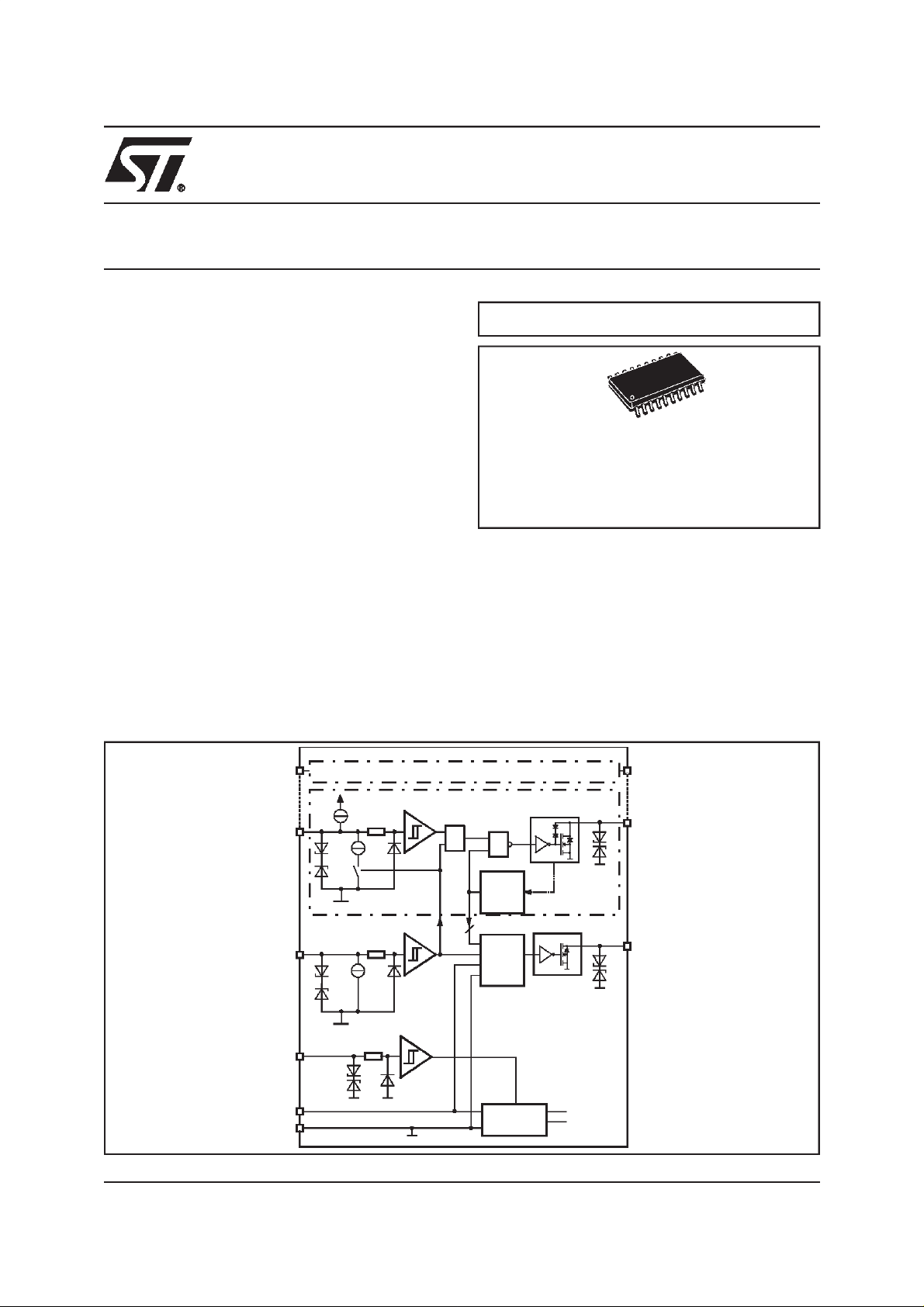
BLOCK DIAGRAM
IN 4
IN 1
PRG
EN
VS
GND
January 2000
This ispreliminary information on a new product now in development. Details are subject to change without notice.
CHANNEL4
VS
R
IN
PRG
R
IN
R
EN
=
THERMAL
SHUTDOWN
4
DIAG-
NOSTIC
LOGIC
REFERENCE
&
CHANNEL1
Vint
Vlogic
OUT 4
OUT 1
DIAG
1/13

L9333
PIN CONNECTION (Top view)
1
NC
2
VS
3
NC
4
IN3
5
IN4
6
EN
OUT4
OUT3
GND
7
813
9
10 11
NC
SO 20 STD
PIN FUNCTION
Pin Name Description
20
NC
19
DIAG
18
NC
17
IN2
16
IN1
15
PRG
14
OUT1
DIAG
GND
GND
GND
GND
OUT2
12
NC
NC
1
IN1
2
IN2
3
4
5
6
7
VS
813
IN3
9
10 11
IN4
So 12+4+4
20
PRG
19
OUT1
18
OUT2
17
GND
16
GND
15
GND
14
GND
Med. Power
OUT3
12
OUT4
EN
Package
SO20 SO20 (SO 12+4+4)
VS Supply Voltage 2 8
GND Ground 9 4, 5, 6, 7, 14, 15, 16, 17
EN Enable 6 11
PRG Programming 15 20
DIAG Diagnostic 19 3
IN 1 Input 1 16 1
IN 2 Input 2 17 2
IN 3 Input 3 4 9
IN 4 Input 4 5 10
OUT 1 OUTPUT 1 14 19
OUT 2 OUTPUT 2 13 18
OUT 3 OUTPUT 3 8 13
OUT4 OUTPUT4 7 12
NC Not Connected 1,3,10,11,12,18,20 -
2/13

ABSOLUTEMAXIMUM RATINGS
Symbol Parameter Value Unit
L9333
V
dV
S
V
IN,VEN
V
PRG
V
OUT
V
DIAG
Notes: 1. In flybackphase the output voltage can reach 60V.
Supply voltage DC
S
Supply voltage Pulse (T = 400ms)
-0.3 to 32
-0.3 to 45
/dt Supply voltage transient -10 to +10 V/µs
,
Input, Enable, Programming
-14to 45 V
Pin voltage
Output voltage
-0.3 to 45
1)
Diagnostic output voltage -0.3 to 45 V
V
V
V
ESD - PROTECTION
Parameter
Supply pins and signal pins ± 2KV
Output pins ± 4KV
Note: Human-Body-Model according to MIL 8832. The device widthstand ST1 classlevel.
Value
against GND
Unit
THERMAL DATA
Symbol Parameter Min Typ Max Unit
T
T
JSDhys
JSD
Temperature shutdown threshold 175 220 °C
Temperature shutdown hysteresis 20 K
SO 12+4+4
R
th (j-p)
R
th (j-a)
Thermal resistance junction to pins 15 °C/W
Thermal resistance junction to ambient
SO 20
R
th (j-a)
2. With 6cm2on board heat sink area.
3. Mounted on SMPCB2board
Thermal resistance junction to ambient
2)
3)
50 °C/W
97 °C/W
3/13

L9333
LIFE TIME
Symbol Parameter Condition Value Unit
t
B
useful life time VS≤ 14V
20 years
EN = low
t
b
operating life time 4.5V ≤ VS≤ 32V
5000 hours
EN = high
OPERATINGRANGE:
Within the operating range the IC operates as described in the circuit description, including the diagnostic table.
Symbol Parameter Condition Min Max Unit
V
V
IN,VEN
V
PRG
V
OUT
S
Supply voltage 4.5 32 V
,
Input voltage -14 45 V
Output voltage Voltage will be limited by internal Z-
-0.3 60 V
Diode clamping
V
DIAG
T
J
Diagnostic output voltage -0.3 45 V
Junction temperature -40 150 °C
ELECTRICAL CHARACTERISTCS
The electrical characteristics are valid within the defined Operating Conditions, unless otherwise specified.
The function is guaranteed by design until T
Symbol Parameter Test Condition Min. Typ. Max. Unit
switch-on-threshold.
JSDon
SUPPLY
Quiescent current VS≤ 14V; VEN≤ 0.3V
I
Q
85 °C
T
amb
V
14V; V
≤
S
150°C
T
a
V
14V;EN = high, Output = off
≤
S
EN
≤
0.3V
<2 10 µA
12
EN = high, Output = on
Inputs, IN1 - IN4;Programming, PRG
V
V
INhigh
R
INlow
Input voltage LOW -14 1 V
Input voltage HIGH 2 45 V
I
Input current
IN
Input impedance VIN< 0V; VIN>V
IN
4. Current direction depends on the programming setting (PRG=high leads into a positive current see also Blockdiagram page 1)
0V ≤ V
IN
≤ 45V
4)
S
-25 50 µA
10 60 kΩ
50 µA
mA
3.5
mA
4/13
 Loading...