

DUALHIGH CURRENT RELAYDRIVER
.HIGH OUTPUT CURRENT
.HYSTERESIS INPUT COMPARATOR WITH
WIDERANGE COMMON MODE OPERATION
ANDGROUNDCOMPATIBLEINPUTS
.INPUTCOMPARATORHYSTERESIS
.INTERNAL THERMAL PROTECTION WITH
HYSTERESIS
.INTERNALOUTPUTOVERVOLTAGECLAMP-
ING
.SINGLESUPPLYVOLTAGE(3.5Vup to18V)
L9305A
Powerdip(8 + 8)
ORDERING NUMBER : L9305A
DESCRIPTION
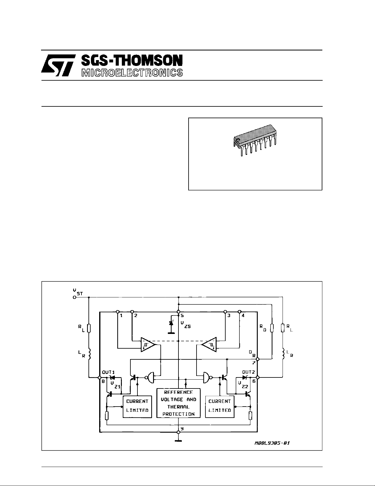
TheL9305Aisa monolithicinterfacecircuit withdifferentialinput comparatorandopencollectoroutput
ableto sink highcurrentspecifically todrive relays,
lamps,d.c. motors.
Particularcarehasbeen takento protectthedevice
againstdestructivefailures - shortcircuit ofoutputs
, outputovervoltages,supplyovervoltage.
toV
S
BLOCK DIAG RAM
A built inthermalshut-downswitchesoff thedevice
whentheIC’sinternaldissipationbecomestoogreat
and the chip temperature exceeds a set security
threshold.
A hysteresisinputcomparatorincreasestheinterface’snoiseimmunity, allowingthecorrectusealsoin
criticalenvironmentsasautomotiveor industrialapplications.
January1992
This is advanced information on a new product now in development or undergoing evaluation. Details are subject to change without notice.
1/6
L9305A
ABSOLUTE MAXIMUM RATINGS
Symbol Parameter Value Unit
V
5
V
7
I
ZS
V
I
V
I
T
j,Tstg
P
tot
I
o
(*) The maximum allowed supply voltage without series resistors is limited by the built-in zener protection diodes
≤ 2.5 ms ; repetition time ≥ 30 m s.
(**) T
on
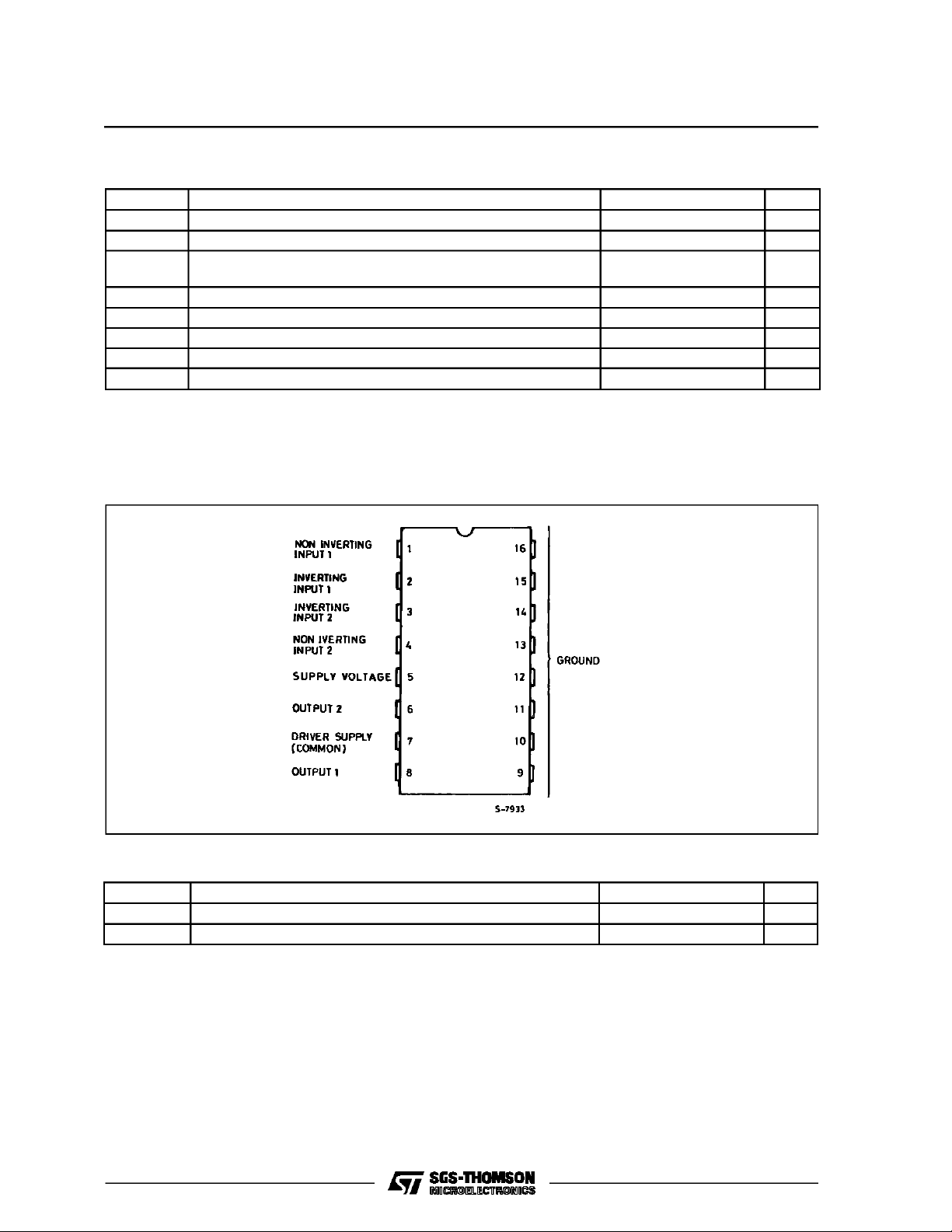
PIN CO NNECT IO N (top view)
Supply Voltage (*) 20 V
Driver Supply Voltage 26 V
Supply Zener Clamp Current (DC)
(PULSED) (**)
30
80
Comparator Input Voltage Range – 0.2 to 24 V
Differential Input Voltage 24 V
Junction and Storage Temperature – 55 to 150 °C
Power Dissipation at T
=85°C 928 mW
amb
Output Current Int. limited
mA
mA
THERMALDATA
Symbol Parameter Value Unit
Thermal Resistance Junction to pins Max. 15 °C/W
Thermal Resistance Junction to Ambient Max. 70 °C/W
2/6
R
th j-pins
R
th j-amb
 Loading...