

■ OPERATING SU PPLY VOLTAGE 5V TO 28V
■ TYPICAL R
= 150 mΩ FOR EACH
DSon
OUTPUT TRANSISTOR (AT 25°C)
■ CONTINOUS DC LOAD CURRENT 5A
(T
< 100 °C)
case
■
OUTPUT CURRENT LIMITATION AT TYP. 6A
■ SHORT CIRCUIT SHUT DOWN FOR OUTPUT
CURRENTS OVER 8A
■ LOGIC- INPUTS TTL/CMOS-COMPATIBLE
■ OPERATING-FREQUENCY UP TO 30 kHz
■ OVER TEMPERATURE PROTECTION
■ SHORT CIRCUIT PROTECTION
■ UNDERVOLTAGE DISABLE FUNCTION
■ DIAGNOSTIC BY SPI OR STATUS-FLAG
(CONFIGURABLE)
■ ENABLE AND DISABLE INPUT
■ SO20 POWER PACKAGE
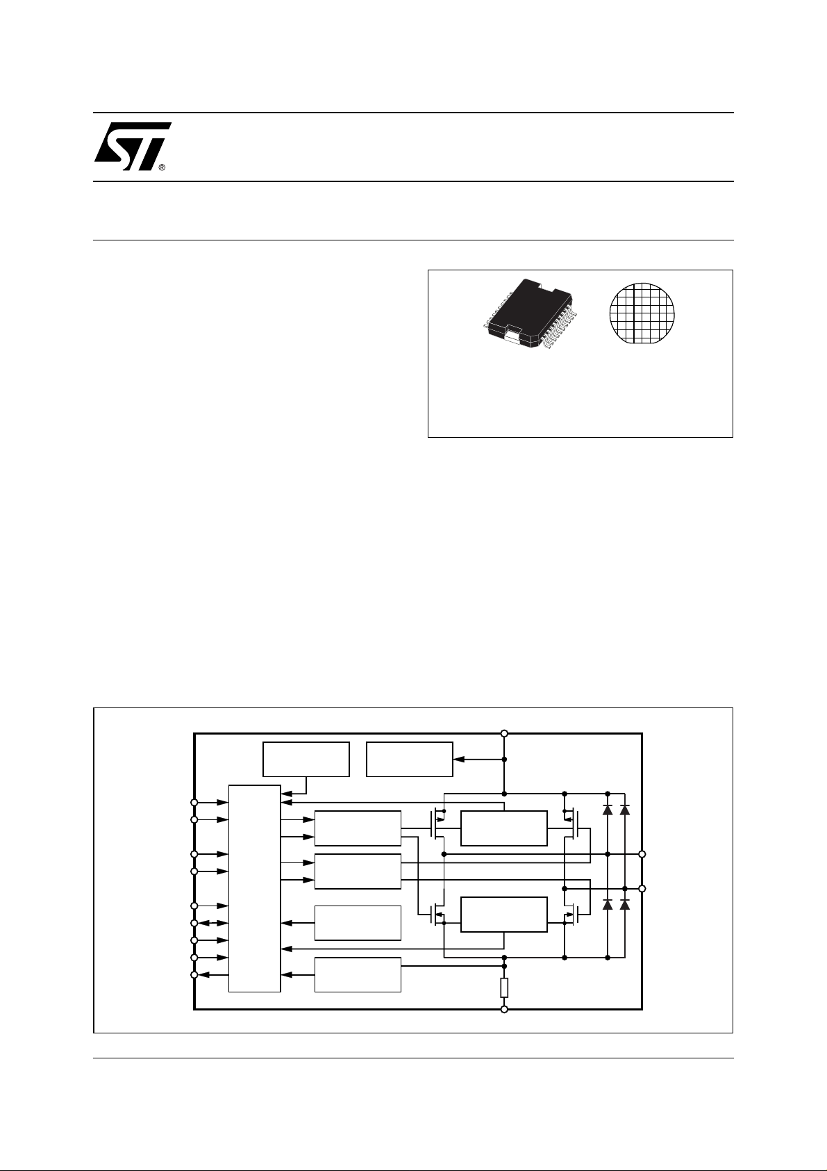
DESCRIPTION
The L9230 is an SPI controlled H-Bridge, designed
for the control of DC and stepper motors in safety critical applications and under extreme environmental
conditions.
L9230
SPI CONTROLLED H-BRIDGE
PRELIMINARY DATA
PowerSO20 BARE-DIE
ORDERING NUMBERS:
L9230 L9230-DIE1
The H-Bridge is protected against over temperature
and short circuits and has an under voltage lockout
for all the supply voltages ”V
ply). All malfunc tions cause the output stages to go
tristate.
The H-Bridge contains integrated free-wheel diodes.
In case of free-wheeling conditi on, the lowside t ransistor is switched on in parallel of its diode to reduce
the current injected into the substrate.
Switching in parallel is only all owed, if the voltagelevel of the according output-stage is below the
ground-level.In this case it must be ensured, that the
upper transistor is switched off.
” (Main DC power sup-
S
BLOCK DIAGRAM
V
S
1
2
OVER
INTERNAL 5V
SUPPLY
OVERCURRENT
HIGH-SIDE
OVERCURRENT
LOW-SIDE
GND
OUT1
OUT2
D01AT470A
UNDERVOLTAGE
V
S
IN1
IN2
DI
EN
LOGIC
DMS
SF/SCK
SS
SI
SO
GATE CONTROL
GATE CONTROL
TEMPERATURE
MAXIMUM
CURRENT
LIMITATION
March 2003
This is preliminary information on a new product now in development or undergoing evaluation. Details are subject to change without notice.
1/25
L9230
PIN FUNCTION
N° Pin Description
1 GND Ground
2 SCK/SF SPI-Clock/Status-flag
3 IN1 Input 1
4V
5 V
6 OU1 Output 1
7 OU1 Output 1
8 SO serial out
9 SI serial in
10 GND Ground
11 GND Ground
12 DMS Diagnostic-Mode selection (+ Supply Voltage for SPI-Interface)
13 EN Enable
14 OU2 Output 2
15 OU2 Output 2
16 V
17 SS Slave select
18 DI Disable
19 IN2 Input 2
20 GND Ground
Supply voltage
S
Supply voltage
S
Supply voltage
S
PIN CONNECTION
(Top view)
GND
SCK
IN1
V
V
OU1
OU1
SO
GND 10
SI
1
2
3
S
S
4
5
6
7
8
9
D01AT471
20
19
18
17
16
15
14
13
12
11
GND
IN2
DI
SS
V
S
OU2
OU2
EN
DMS
GND
2/25
L9230
ABSOLUTE MAXIMUM RATINGS
The integrated circuit must not be destroyed by use at the limit values.
Each limit value can be used, as long as no other limit is violated.
Voltage reference point: All values are, if not otherwise stated, relative to ground.
Direction of current flow: Current flow into a pin is positive.
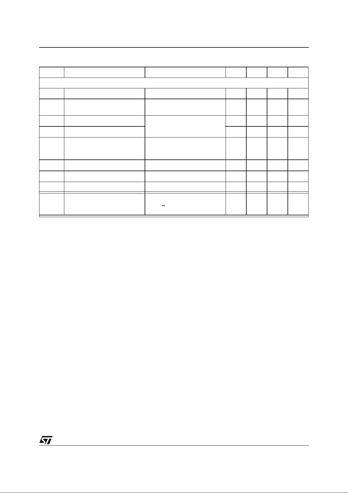
Rise-, fall- and delaytimes: If not otherwise stated, all rise times are between 10% and 90%, fall times
between 90% and 10% and delay times at 50% of the relevant steps.
Symbol Parameter Test Condition Min. Typ. Max. Unit
V
V
V
THERMAL DATA
Symbol Parameter Test Condition Min. Typ. Max. Unit
T
T
R
th j-case
T
Supply voltage static destruction proof -1 40 V
S
dynamic destruction proof t <0.5s
-2 40 V
(single pulse, Tj < 85°C)
LI
Logic inputs
-0.5 7 V
IN1, IN2, DI, EN, SS, SI, SCK,DMS
I
Logic inputs
LI
IN1, IN2, DI, EN, SS, SI, SCK,DMS
Logic outputs SF, SO R ≥ 10kΩ -0.5 7 V
LO
Junction temperature
T
j
-40 +150
dynamic t < 1 s
Storage temperature -55 +125 °C
stg
Ambient temperature -40 +125 °C
amb
Thermal resistance junction to
(2)
case
Thermal Shutdown Junction
j_sd
165 175 °C
Temperature Threshold
-20 mA
+175
3 °C/W
°C
°C
ELECTRICAL CHARACTERISTCS
( Tj = -40 to +150°C; VS = 5 to 28V)
Symbol Parameter Test Condition Min. Typ. Max. Unit
Power Supply
V
Supply Voltage Static Condition 5 28 V
S
Dynamic Condition (t < 500ms) 40 V
Undervoltage Shutdow n
(at least down to 2.5V)
(1)
4.7 5 V
Switch OFF voltage 4.5 5 V
Switch ON voltage 4.7 5 V
Hysteresis 200 mV
I
Supply current f = 0 kHz, IO = 0 A
S
f = 20kHz, IO = 0 A
Note: 1. For supply volt ag es d own to 2.5 V t he ou tp ut s tage s ar e in trist ate cond itio n and t he st atus flag is set to lo w. B e low 2 .5V the
device op erates in unde fined condition
2. Guaranteed by d esign and package characterization
13
30
mA
mA
3/25
L9230
ELECTRICAL CHARACTERISTCS
( Tj = -40 to +150°C; VS = 5 to 28V)
(continued)
Symbol Parameter Test Condition Min. Typ. Max. Unit
Logic inputs
V
Logic Input Voltage
I
1 1.5 2 V
IN1, IN2, DI, EN
Logic Input Current
I
I
VI ≤ 1V -200 -125 µA
IN1, IN2, DI
I
Input Current EN V
EN
Detection Time EN, DI 3 4 µs
t
dt
≥ 2V 75 100 µA
IEN
Power Outputs (OUT1, OUT2)
R
Switch on Resistance LS R
S
Switch on Resistance HS R
, VS > 5 V 150 250 mΩ
OUT-Vs
OUT-GND, VS
> 5 V 150 250 mΩ
Current Limitation Peak value controlled
inductive load L = 0,8 to 5 mH
resistive load R = 0,8 to 1.8 Ω
|I
OU|max
|IOU|
t
a/tb
Switch-off Current -40 °C < Tj < 165 °C
max
t
a
t
b
Switch-off time
Blanking time
Tracking
(2)
(2)
(2)
Tj < 175 °C
5.5 6
7.7 A
2.5
12 17 22 µs
811.515µs
1.4 1.5 1.6
A
|
|I
OUK
∆|I
Short circuit detection curren t
|
OUK
Short Circuit Current Trecking
t Reactivation time after internal
(2)
(2)
(3 )
I
L
V
FD
t
rr
V
SFHigh
|I
ou| max
I
SF
I
SF
shut down
Leakage Current Output stage switched off 1 mA
Free-wheel diode forward voltage IO = 3A, VS = 0V 2 V
Free-wheel diode reverse
recovery time
Output„high“ (SF not set)
Switch OFF Current Tj = -40 to 165°C 6 A
Output„high“ (SF not set)
Output„low“ (SF set)
(*)
(2)
(1)
see figure 1 5.5 11 A
(1)
1600 mA
Overcurrent- or overtemperature
shut down to reactivation of the
output stage
VS = 5V, R
= 27KΩ 4.1 V
Pull_up
Tj = < 175°C 2.5 A
V
= 5V 20 µA
SF
V
= 1V 300 µA
SF
V
= 0.5V 100 µA
SF
V
= 0.8V 500 µA
SF
1ms
100 ns
4/25
L9230
ELECTRICAL CHARACTERISTCS
( Tj = -40 to +150°C; VS = 5 to 28V)
(continued)
Symbol Parameter Test Condition Min. Typ. Max. Unit
Timing
f PWM Frequency min. operating time 10µs 2 30 kHz
f
Switching Frequency during
S
5 30 kHz
current limitation
t
don
t
doff
t
Output ON-delay
IN1 --> OUT1 or IN2 --> OUT2
35µs
Output OFF-delay 3 5 µs
, t
Output rise-, fall Time
r
f
OUT1H--> OUT1L, OUT2H--> OUT2L,
0.2 0.4 1 µs
IOUT = 3 A
OUT1L--> OUT1H, OUT2L--> OUT2H
t
ddis
t
Disable Delay Time DIn --> OUTn, En --> OUTn 3 4 µs
Power on Delay Time VS = on --> output stage active 15 ms
dp
Delay time for fault detection 5 15 µs
|∆I| Effect of reverse current at power
supply
(*) For low er pull up resis tances than 27kΩ the specified value of xxxV (minimum) is guaranteed by design
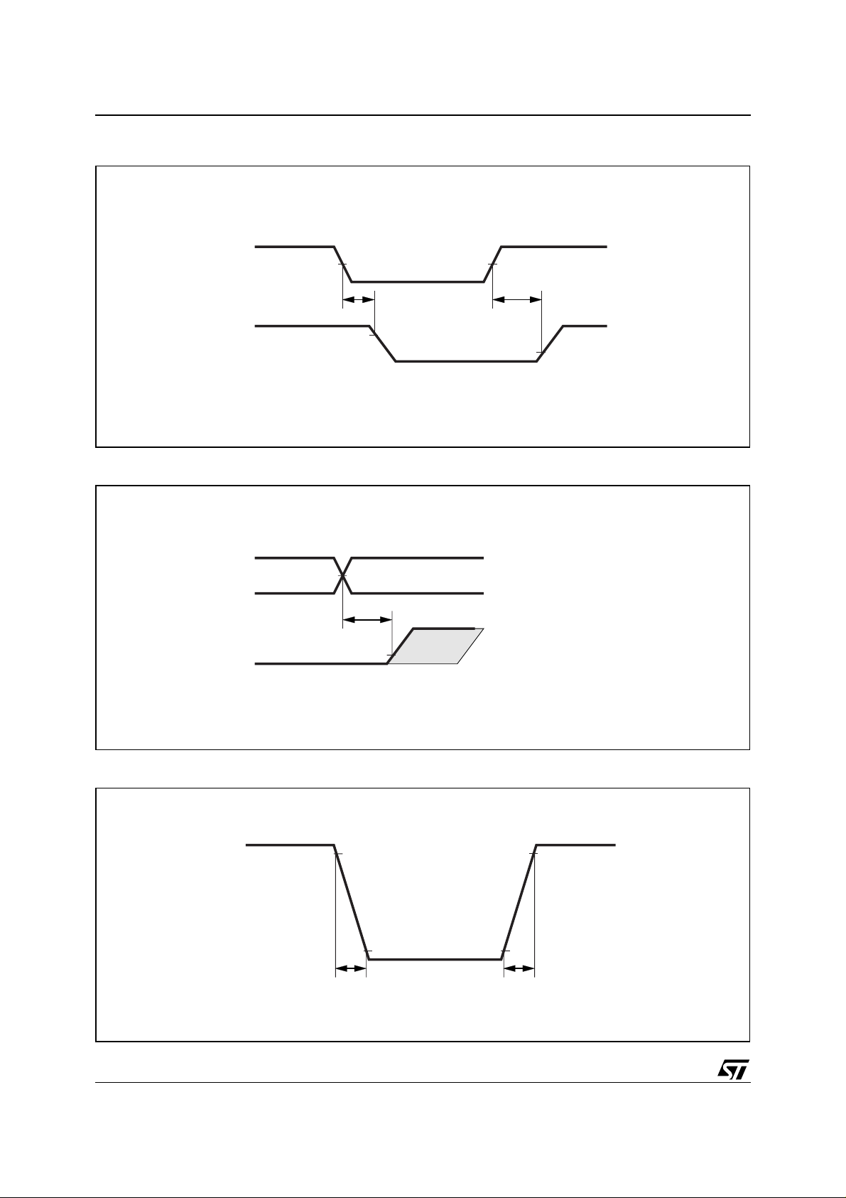
Note: 1. In case of SC OUTx to Vs the switch off current is always higher than the start value of current regulation (∆|I
2. Guaranteed by design
3. Value is tested down to 6V. For supply voltage below 6V on i ncreased current can be fed bac k in the device via a pro tection path
4,5V < V
- IVs < 3A
∆
I for ISI, ISO, ISS, I
DMS
< 5,5V
SCK
, I
, I
, IEN,I
IN1
IN2
DI
100 µA
| = |I
OUK
OUK
| - |I
OUmax
|
5/25
L9230
Figure 1. Out put del a y t ime
IN
n
OUT
n
Figure 2. Dis abl e del a y tim e
DI
n
OUT
n
50%
t
don
50%
t
ddis
10%
90%
Z
D01AT473
50%
t
doff
10%
D01AT472
Figure 3. Out put sw i tchi ng time
OUT
n
6/25
90% 90%
10%
t
f
t
r
D01AT474
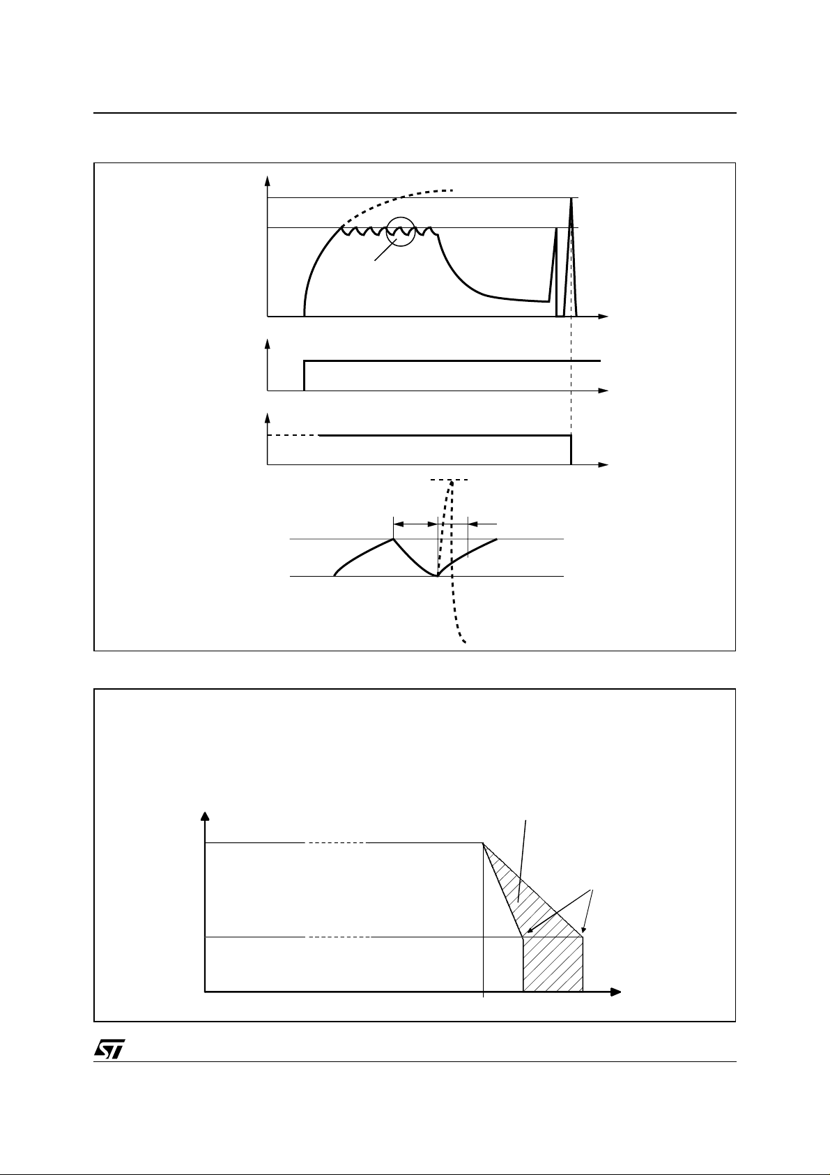
Figure 4.
L9230
LOAD
CURRENT
>8A
typ 6.6A
CONTROL
SIGNAL
STATUS
FLAG
DETAIL A
6.6A
CURRENT LIMITATION
A
t
a
OVERCURRENT
DETECTION
t
b
OVERCURRENT
ta = SWITCH_OFF TIME IN CURRENT LIMITATION
tb = CURRENT LIMITATION BLANKING TIME
D01AT475
Figure 5.
Temperature-depending current-limitation
Maximum rating for junction temperature for < 1s 175°C
Overtemperature switch-off > 175°C
Switch-off current in case of current limitation 6,6A ± 1,1A Tj < 165°C
For 165°C < Tj < 175°C the maximum current decreases from Imax. = 6,6A ± 1,1A to Imax. = 2,5A ± 1,1A.
Tolerance-range
Imax
6.6A
2.5A
of temperat u re -depen de nt
current - reduc tion
165°C
175°C
Range of
Overtemperatur e
switch-off
Tj
7/25
L9230
ELECTRICAL CHARACTERISTICS
(continued)
SPI INTERFACE
The timing of L9230 is defined as follows:
- The change at output (SO) is forced by the rising edge of the SCK signal.
- The input signal (SI) is taken over on the falling edge of the SCK signal.
= active without any clocks at SCK is not allowed
- SS
- The data received during a writing access is taken over into the internal registers on the rising edge of the SS
signal, if exactly 16 SPI clocks have been counted duri ng SS
= active.
Figure 6.
910
SS
SCK
2
11
1
4
3
8
12
7
SO
SI
5
MSB IN
tristate
6
Bit (n-3)
Bit (n-3)Bit (n-2)
Bit (n-4)...1
Bit (n-4)...1
Bit 0; LSB
LSB IN
n = 16
ELECTRICAL CHARACTERISTCS
( continued)
Symbol Parameter Test Condition Min. Typ. Max. Unit
Input SCK
V
SCKL
V
SCKH
∆V
C
SCK
(SPI clock input 4.5V < DMS < 5.5V)
Low Level 1 V
High Level 2 V
Hysteresis 0.1 0.4 V
SCK
Input Capacity 10 pF
8/25
 Loading...