

Datasheet L78S10T, L78S09CV, L78S09CT, L78S05T, L78S05CV Datasheet (SGS Thomson Microelectronics)
...
L78S00
SER IES
January 1993
2A POSITIVEVOLTAGE REGULATORS
.OUTPUTCURRENT TO 2A
.OUTPUTVOLTAGESOF5;7.5; 9; 10;12; 15;
18 ; 24V
.THERMALOVERLOAD PROTECTION
.SHORTCIRCUIT PROTECTION
.OUTPUTTRANSISTOR SOA PROTECTION
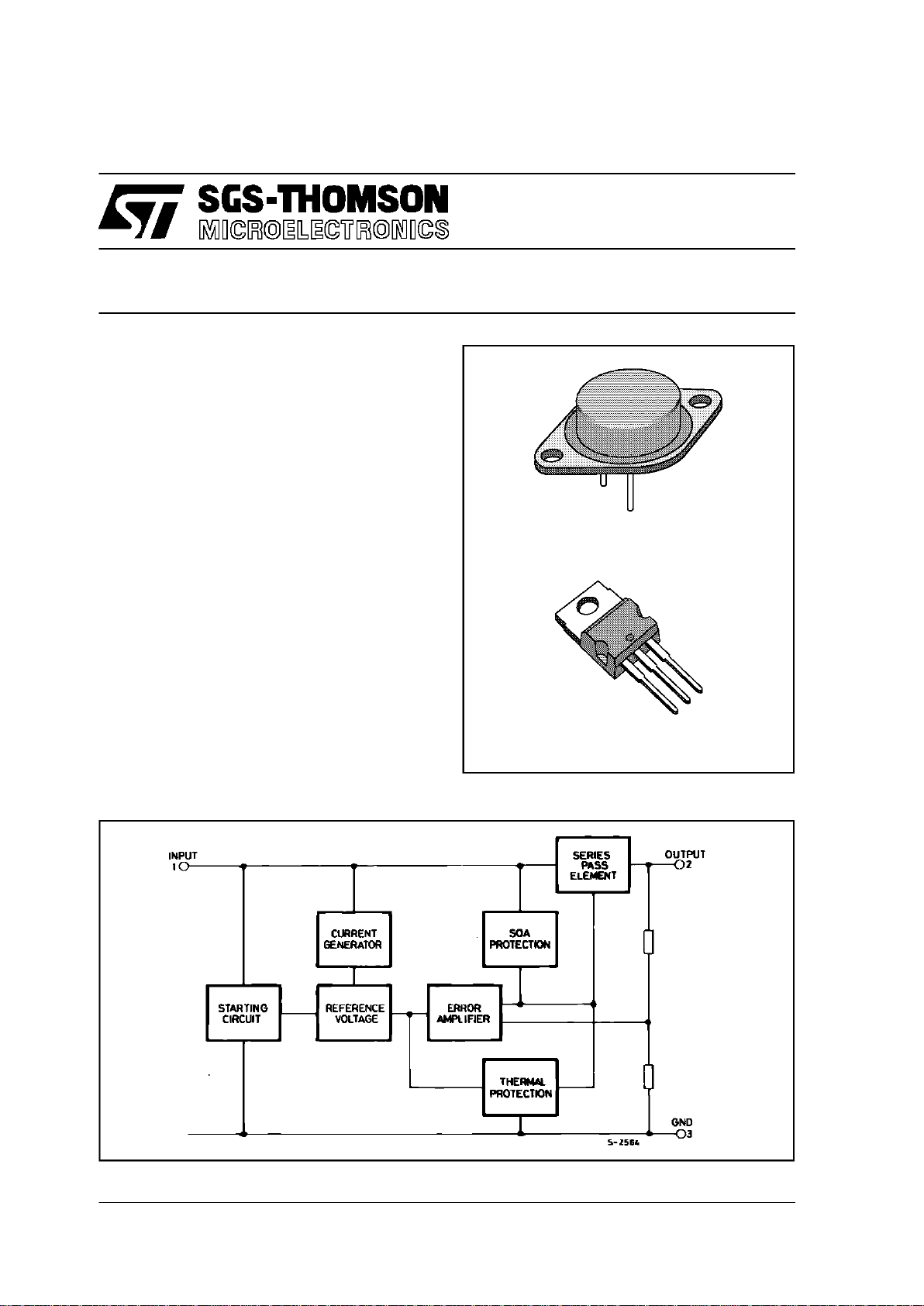
DESCRIPTION
The L78S00 series ofthree-terminal positive regulators is available in TO-220 and TO-3 packages
and with several fixed output voltages, making it
useful in a widerange of applications. Theseregulators canprovide local on-cardregulation, eliminating the distribution problems associated with single
pointregulation. Eachtypeemploysinternalcurrent
limiting, thermal shut-down and safe area protection,makingitessentially indestructible. Ifadequate
heat sinking is provided, they can deliver over 2A
outputcurrent. Althoughdesigned primarily as fixed
voltage regulators, these devices can be used with
external components to obtain adjustable voltages
and currents.
TO-220
BLOCK DIAGRAM
TO-3
1/21
ABSOLUTE MAXI MUM RAT IN G S
Symbol Parameter Value Unit
V
i
DC Input Voltage (for Vo= 5 to 18V)
(for V
o
=24V)
35
40
V
V
I
o
Output Current Internally limited
P
tot
Power Dissipation Internally limited
T
stg
Storage Temperature – 65 to + 150 °C
T
op
Operating Junction Temperature (for L78S00)
(for L78S00C )
–55to+150
0to+150
°C
°C
THERMALDATA
TO-220 TO-3
R
th j-case
R
th j-amb
Thermal Resistance Junction-case
Thermal Resistance Junction-ambient
Max
Max
3
50
4
35
°C/W
°C/W
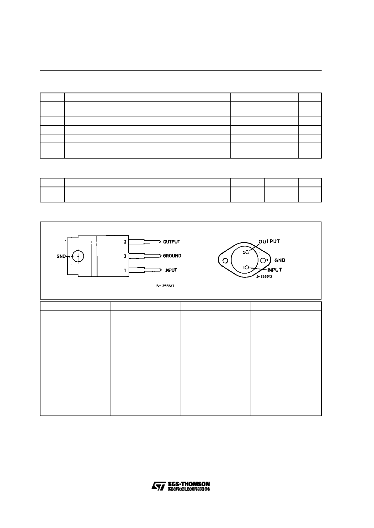
CONN E CTION DIAGRAMS A N D ORDERI NG NUMBERS (top views)
Type TO-220 TO -3 Output Voltage
L78S05
L78S05C
L78S75
L78S75C
L78S09
L78S09C
L78S10
L78S10C
L78S12
L78S12C
L78S15
L78S15C
L78S18
L78S18C
L78S24
L78S24C
L78S05CV
L78S75CV
L78S09CV
L78S10CV
L78S12CV
L78S15CV
L78S18CV
L78S24CV
L78S05T
L78S05CT
L78S75T
L78S75CT
L78S09T
L78S09CT
L78S10T
L78S10CT
L78S12T
L78S12CT
L78S15T
L78S15CT
L78S18T
L78S18CT
L78S24T
L78S24CT
5V
5V
7.5V
7.5V
9V
9V
10V
10V
12V
12V
15V
15V
18V
18V
24V
24V
L78S00 SERIES
2/21
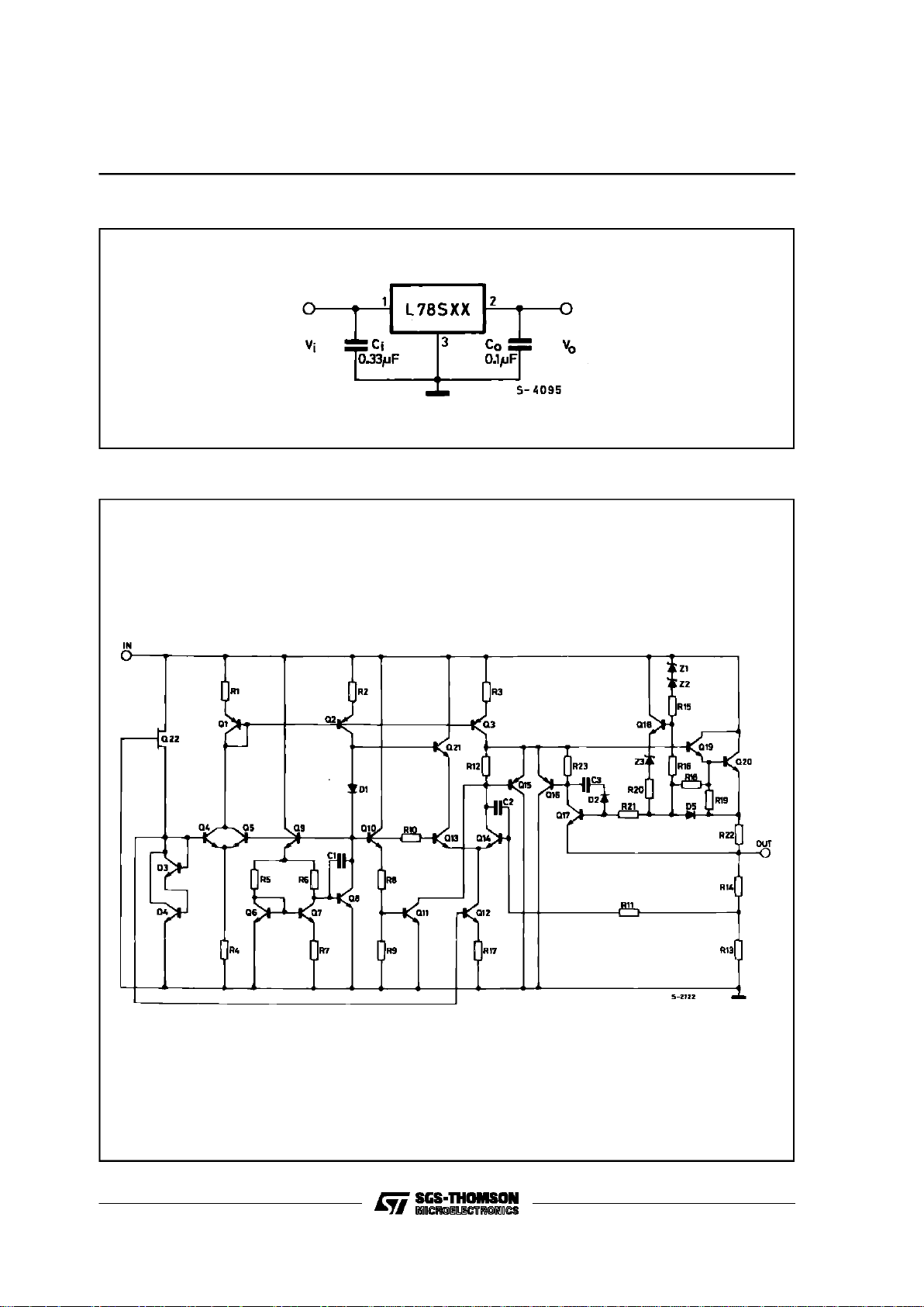
APPLICATION CIRCUIT
SCHEMAT IC D I AGRAM
L78S00 SERIES
3/21
TEST CIRCUI TS
Figure 1 : DC Parameters. Figure 2 : Load Regulation.
Figure 3 : Ripple Rejection.
L78S00 SERIES
4/21

ELECTRICAL CHARACTERISTICS FOR L78S05 (refer to the test circuits, Tj=25oC,
Vi= 10V, Io= 500 mA unless otherwise specified)
Symbol Parameter Test Conditions Min. Typ. Max. Unit
V
o
Output Voltage 4.8 5 5.2 V
V
o
Output Voltage Io=1A Vi= 7 V 4.75 5 5.25 V
∆V
o
Line Regulation Vi= 7 to 25 V
Vi= 8 to 25 V
100
50
mV
mV
∆V
o
Load Regulation Io= 20 mA to 2 A 100 mV
I
d
Quiescent Current 8mA
∆I
d
Quiescent Current Change Io= 20 mA to 1A 0.5 mA
∆I
d
Quiescent Current Change Io=20mA Vi= 7 to 25 V 1.3 mA
∆
V
o
∆
T
Output Voltage Drift Io= 5 mA Tj= -55 to 150oC -1.1 mV/oC
e
N
Output Noise Voltage B = 10Hz to 100KHz 40 µV
SVR Supply Voltage Rejection f = 120 Hz 60 dB
V
i
Operating Input Voltage Io≤ 1.5 A 8 V
R
o
Output Resistance f = 1KHz 17 mΩ
I
sc
Short Circuit Current Vi= 27 V 500 mA
I
scp
Short Circuit Peack Current 3 A
ELECTRICAL CHARACTERISTICS FOR L78S75 (refer to the test circuits, Tj=25oC,
Vi= 12.5V, Io= 500 mA unless otherwise specified)
Symbol Parameter Test Conditions Min. Typ. Max. Unit
V
o
Output Voltage 7.15 7.5 7.9 V
V
o
Output Voltage Io=1A Vi= 9.5 V 7.1 7.5 7.95 V
∆V
o
Line Regulation Vi= 9.5 to 25 V
V
i
= 10.5 to 20 V
120
60
mV
mV
∆V
o
Load Regulation Io= 20 mA to 2 A 120 mV
I
d
Quiescent Current 8mA
∆I
d
Quiescent Current Change Io= 20 mA to 1A 0.5 mA
∆I
d
Quiescent Current Change Io=20mA Vi= 9.5 to 25 V 1.3 mA
∆
V
o
∆
T
Output Voltage Drift Io= 5 mA Tj= -55 to 150oC -0.8 mV/oC
e
N
Output Noise Voltage B = 10Hz to 100KHz 52 µV
SVR Supply Voltage Rejection f = 120 Hz 54 dB
V
i
Operating Input Voltage Io≤ 1.5 A 10.5 V
R
o
Output Resistance f = 1KHz 16 mΩ
I
sc
Short Circuit Current Vi= 27 V 500 mA
I
scp
Short Circuit Peack Current 3 A
L78S00 SERIES
5/21
ELECTRICAL CHARACTERISTICS FOR L78S09 (refer to the test circuits, Tj=25oC,
Vi= 14V, Io= 500 mA unless otherwise specified)
Symbol Parameter Test Conditions Min. Typ. Max. Unit
V
o
Output Voltage 8.65 9 9.35 V
V
o
Output Voltage Io=1A Vi= 11 V 8.6 9 9.4 V
∆V
o
Line Regulation Vi=11to25V
Vi=11to20V
130
65
mV
mV
∆V
o
Load Regulation Io= 20 mA to 2 A 130 mV
I
d
Quiescent Current 8mA
∆I
d
Quiescent Current Change Io= 20 mA to 1A 0.5 mA
∆I
d
Quiescent Current Change Io=20mA Vi= 11 to 25 V 1.3 mA
∆
V
o
∆
T
Output Voltage Drift Io= 5 mA Tj= -55 to 150oC -1 mV/oC
e
N
Output Noise Voltage B = 10Hz to 100KHz 60 µV
SVR Supply Voltage Rejection f = 120 Hz 53 dB
V
i
Operating Input Voltage Io≤ 1.5 A 12 V
R
o
Output Resistance f = 1KHz 17 mΩ
I
sc
Short Circuit Current Vi= 27 V 500 mA
I
scp
Short Circuit Peack Current 3 A
ELECTRICAL CHARACTERISTICS FOR L78S10 (refer to the test circuits, Tj=25oC,
Vi= 15V, Io= 500 mA unless otherwise specified)
Symbol Parameter Test Conditions Min. Typ. Max. Unit
V
o
Output Voltage 9.5 10 10.5 V
V
o
Output Voltage Io=1A Vi= 12.5 V 9.4 10 10.6 V
∆V
o
Line Regulation Vi= 12.5 to 30 V
V
i
=14to22V
200
100
mV
mV
∆V
o
Load Regulation Io= 20 mA to 2 A 150 mV
I
d
Quiescent Current 8mA
∆I
d
Quiescent Current Change Io= 20 mA to 1A 0.5 mA
∆I
d
Quiescent Current Change Io=20mA Vi= 12.5 to 30 V 1 mA
∆
V
o
∆
T
Output Voltage Drift Io= 5 mA Tj= -55 to 150oC -1 mV/oC
e
N
Output Noise Voltage B = 10Hz to 100KHz 65 µV
SVR Supply Voltage Rejection f = 120 Hz 53 dB
V
i
Operating Input Voltage Io≤ 1.5 A 13 V
R
o
Output Resistance f = 1KHz 17 mΩ
I
sc
Short Circuit Current Vi= 27 V 500 mA
I
scp
Short Circuit Peack Current 3 A
L78S00 SERIES
6/21

ELECTRICAL CHARACTERISTICS FOR L78S12 (refer to the test circuits, Tj=25oC,
Vi= 19V, Io= 500 mA unless otherwise specified)
Symbol Parameter Test Conditions Min. Typ. Max. Unit
V
o
Output Voltage 11.5 12 12.5 V
V
o
Output Voltage Io=1A Vi= 14.5 V 11.4 12 12.6 V
∆V
o
Line Regulation Vi= 14.5 to 30 V
Vi=16to22V
240
120
mV
mV
∆V
o
Load Regulation Io= 20 mA to 2 A 160 mV
I
d
Quiescent Current 8mA
∆I
d
Quiescent Current Change Io= 20 mA to 1A 0.5 mA
∆I
d
Quiescent Current Change Io=20mA Vi= 14.5 to 30 V 1 mA
∆
V
o
∆
T
Output Voltage Drift Io= 5 mA Tj= -55 to 150oC -1 mV/oC
e
N
Output Noise Voltage B = 10Hz to 100KHz 75 µV
SVR Supply Voltage Rejection f = 120 Hz 53 dB
V
i
Operating Input Voltage Io≤ 1.5 A 15 V
R
o
Output Resistance f = 1KHz 18 mΩ
I
sc
Short Circuit Current Vi= 27 V 500 mA
I
scp
Short Circuit Peack Current 3 A
ELECTRICAL CHARACTERISTICS FOR L78S15 (refer to the test circuits, Tj=25oC,
Vi= 23V, Io= 500 mA unless otherwise specified)
Symbol Parameter Test Conditions Min. Typ. Max. Unit
V
o
Output Voltage 14.4 15 15.6 V
V
o
Output Voltage Io=1A Vi= 17.5 V 14.25 15 15.75 V
∆V
o
Line Regulation Vi= 17.5 to 30 V
V
i
=20to26V
300
150
mV
mV
∆V
o
Load Regulation Io= 20 mA to 2 A 180 mV
I
d
Quiescent Current 8mA
∆I
d
Quiescent Current Change Io= 20 mA to 1A 0.5 mA
∆I
d
Quiescent Current Change Io=20mA Vi= 17.5 to 30 V 1 mA
∆
V
o
∆
T
Output Voltage Drift Io= 5 mA Tj= -55 to 150oC -1 mV/oC
e
N
Output Noise Voltage B = 10Hz to 100KHz 90 µV
SVR Supply Voltage Rejection f = 120 Hz 52 dB
V
i
Operating Input Voltage Io≤ 1.5 A 18 V
R
o
Output Resistance f = 1KHz 19 mΩ
I
sc
Short Circuit Current Vi= 27 V 500 mA
I
scp
Short Circuit Peack Current 3 A
L78S00 SERIES
7/21

ELECTRICAL CHARACTERISTICS FOR L78S18 (refer to the test circuits, Tj=25oC,
Vi= 26V, Io= 500 mA unless otherwise specified)
Symbol Parameter Test Conditions Min. Typ. Max. Unit
V
o
Output Voltage 17.1 18 18.9 V
V
o
Output Voltage Io=1A Vi= 20.5 V 17 18 19 V
∆V
o
Line Regulation Vi= 20.5 to 30 V
Vi=22to28V
360
180
mV
mV
∆V
o
Load Regulation Io= 20 mA to 2 A 200 mV
I
d
Quiescent Current 8mA
∆I
d
Quiescent Current Change Io= 20 mA to 1A 0.5 mA
∆I
d
Quiescent Current Change Io=20mA Vi=22to33V 1 mA
∆
V
o
∆
T
Output Voltage Drift Io= 5 mA Tj= -55 to 150oC -1 mV/oC
e
N
Output Noise Voltage B = 10Hz to 100KHz 110 µV
SVR Supply Voltage Rejection f = 120 Hz 49 dB
V
i
Operating Input Voltage Io≤ 1.5 A 21 V
R
o
Output Resistance f = 1KHz 22 mΩ
I
sc
Short Circuit Current Vi= 27 V 500 mA
I
scp
Short Circuit Peack Current 3 A
ELECTRICAL CHARACTERISTICS FOR L78S24 (refer to the test circuits, Tj=25oC,
Vi= 33V, Io= 500 mA unless otherwise specified)
Symbol Parameter Test Conditions Min. Typ. Max. Unit
V
o
Output Voltage 23 24 25 V
V
o
Output Voltage Io=1A Vi= 27 V 22.8 24 25.2 V
∆V
o
Line Regulation Vi=27to38V
V
i
=30to36V
480
240
mV
mV
∆V
o
Load Regulation Io= 20 mA to 2 A 250 mV
I
d
Quiescent Current 8mA
∆I
d
Quiescent Current Change Io= 20 mA to 1A 0.5 mA
∆I
d
Quiescent Current Change Io=20mA Vi= 8 to 25 V 1 mA
∆
V
o
∆
T
Output Voltage Drift Io= 5 mA Tj= -55 to 150oC -1.5 mV/oC
e
N
Output Noise Voltage B = 10Hz to 100KHz 170 µV
SVR Supply Voltage Rejection f = 120 Hz 48 dB
V
i
Operating Input Voltage Io≤ 1.5 A 27 V
R
o
Output Resistance f = 1KHz 23 mΩ
I
sc
Short Circuit Current Vi= 27 V 500 mA
I
scp
Short Circuit Peack Current 3 A
L78S00 SERIES
8/21

ELECTRICAL CHARACTERISTICS FOR L78S05C (refer to the test circuits, Tj=25oC,
Vi= 10V, Io= 500 mA unless otherwise specified)
Symbol Parameter Test Conditions Min. Typ. Max. Unit
V
o
Output Voltage 4.8 5 5.2 V
V
o
Output Voltage Io=1A Vi= 7 V 4.75 5 5.25 V
∆V
o
Line Regulation Vi= 7 to 25 V
Vi= 8 to 12 V
100
50
mV
mV
∆V
o
Load Regulation Io= 20 mA to 1.5 A
Io=2A 80
100 mV
I
d
Quiescent Current 8mA
∆I
d
Quiescent Current Change Io= 20 mA to 1A 0.5 mA
∆I
d
Quiescent Current Change Io=20mA Vi= 7 to 25 V 1.3 mA
∆
V
o
∆
T
Output Voltage Drift Io= 5 mA Tj= 0 to 70oC -1.1 mV/oC
e
N
Output Noise Voltage B = 10Hz to 100KHz 40 µV
SVR Supply Voltage Rejection f = 120 Hz 54 dB
V
i
Operating Input Voltage Io≤ 1.5 A 8 V
R
o
Output Resistance f = 1KHz 17 mΩ
I
sc
Short Circuit Current Vi= 27 V 500 mA
I
scp
Short Circuit Peack Current 3 A
ELECTRICAL CHARACTERISTICS FOR L78S75C (refer to the test circuits, Tj=25oC,
Vi= 12.5V, Io= 500 mA unless otherwise specified)
Symbol Parameter Test Conditions Min. Typ. Max. Unit
V
o
Output Voltage 7.15 7.5 7.9 V
V
o
Output Voltage Io=1A Vi= 9.5 V 7.1 7.5 7.95 V
∆V
o
Line Regulation Vi= 9.5 to 25 V
V
i
= 10.5 to 20 V
120
60
mV
mV
∆V
o
Load Regulation Io= 20 mA to 1.5 A
Io= 2 A 100
140 mV
I
d
Quiescent Current 8mA
∆I
d
Quiescent Current Change Io= 20 mA to 1A 0.5 mA
∆I
d
Quiescent Current Change Io=20mA Vi= 9.5 to 25 V 1.3 mA
∆
V
o
∆
T
Output Voltage Drift Io= 5 mA Tj= 0 to 70oC -0.8 mV/oC
e
N
Output Noise Voltage B = 10Hz to 100KHz 52 µV
SVR Supply Voltage Rejection f = 120 Hz 48 dB
V
i
Operating Input Voltage Io≤ 1.5 A 10.5 V
R
o
Output Resistance f = 1KHz 16 mΩ
I
sc
Short Circuit Current Vi= 27 V 500 mA
I
scp
Short Circuit Peack Current 3 A
L78S00 SERIES
9/21

ELECTRICAL CHARACTERISTICS FOR L78S09C (refer to the test circuits, Tj=25oC,
Vi= 14V, Io= 500 mA unless otherwise specified)
Symbol Parameter Test Conditions Min. Typ. Max. Unit
V
o
Output Voltage 8.65 9 9.35 V
V
o
Output Voltage Io=1A Vi= 11 V 8.6 9 9.4 V
∆V
o
Line Regulation Vi=11to25V
Vi=11to20V
130
65
mV
mV
∆V
o
Load Regulation Io= 20 mA to 1.5 A
Io= 2 A 100
170 mV
I
d
Quiescent Current 8mA
∆I
d
Quiescent Current Change Io= 20 mA to 1A 0.5 mA
∆I
d
Quiescent Current Change Io=20mA Vi= 11 to 25 V 1.3 mA
∆
V
o
∆
T
Output Voltage Drift Io= 5 mA Tj= 0 to 70oC -1 mV/oC
e
N
Output Noise Voltage B = 10Hz to 100KHz 60 µV
SVR Supply Voltage Rejection f = 120 Hz 47 dB
V
i
Operating Input Voltage Io≤ 1.5 A 12 V
R
o
Output Resistance f = 1KHz 17 mΩ
I
sc
Short Circuit Current Vi= 27 V 500 mA
I
scp
Short Circuit Peack Current 3 A
ELECTRICAL CHARACTERISTICS FOR L78S10C (refer to the test circuits, Tj=25oC,
Vi= 15V, Io= 500 mA unless otherwise specified)
Symbol Parameter Test Conditions Min. Typ. Max. Unit
V
o
Output Voltage 9.5 10 10.5 V
V
o
Output Voltage Io=1A Vi= 12.5 V 9.4 10 10.6 V
∆V
o
Line Regulation Vi= 12.5 to 30 V
V
i
=14to22V
200
100
mV
mV
∆V
o
Load Regulation Io= 20 mA to 1.5 A
Io= 2 A 150
240 mV
I
d
Quiescent Current 8mA
∆I
d
Quiescent Current Change Io= 20 mA to 1A 0.5 mA
∆I
d
Quiescent Current Change Io=20mA Vi= 12.5 to 30 V 1 mA
∆
V
o
∆
T
Output Voltage Drift Io= 5 mA Tj= 0 to 70oC -1 mV/oC
e
N
Output Noise Voltage B = 10Hz to 100KHz 65 µV
SVR Supply Voltage Rejection f = 120 Hz 47 dB
V
i
Operating Input Voltage Io≤ 1.5 A 13 V
R
o
Output Resistance f = 1KHz 17 mΩ
I
sc
Short Circuit Current Vi= 27 V 500 mA
I
scp
Short Circuit Peack Current 3 A
L78S00 SERIES
10/21

ELECTRICAL CHARACTERISTICS FOR L78S12C (refer to the test circuits, Tj=25oC,
Vi= 19V, Io= 500 mA unless otherwise specified)
Symbol Parameter Test Conditions Min. Typ. Max. Unit
V
o
Output Voltage 11.5 12 12.5 V
V
o
Output Voltage Io=1A Vi= 14.5 V 11.4 12 12.6 V
∆V
o
Line Regulation Vi= 14.5 to 30 V
Vi=16to22V
240
120
mV
mV
∆V
o
Load Regulation Io= 20 mA to 1.5 A
Io= 2 A 150
240 mV
I
d
Quiescent Current 8mA
∆I
d
Quiescent Current Change Io= 20 mA to 1A 0.5 mA
∆I
d
Quiescent Current Change Io=20mA Vi= 14.5 to 30 V 1 mA
∆
V
o
∆
T
Output Voltage Drift Io= 5 mA Tj= 0 to 70oC -1 mV/oC
e
N
Output Noise Voltage B = 10Hz to 100KHz 75 µV
SVR Supply Voltage Rejection f = 120 Hz 47 dB
V
i
Operating Input Voltage Io≤ 1.5 A 15 V
R
o
Output Resistance f = 1KHz 18 mΩ
I
sc
Short Circuit Current Vi= 27 V 500 mA
I
scp
Short Circuit Peack Current 3 A
ELECTRICAL CHARACTERISTICS FOR L78S15C (refer to the test circuits, Tj=25oC,
Vi= 23V, Io= 500 mA unless otherwise specified)
Symbol Parameter Test Conditions Min. Typ. Max. Unit
V
o
Output Voltage 14.4 15 15.6 V
V
o
Output Voltage Io=1A Vi= 17.5 V 14.25 15 15.75 V
∆V
o
Line Regulation Vi= 17.5 to 30 V
V
i
=20to26V
300
150
mV
mV
∆V
o
Load Regulation Io= 20 mA to 1.5 A
Io= 2 A 150
300 mV
I
d
Quiescent Current 8mA
∆I
d
Quiescent Current Change Io= 20 mA to 1A 0.5 mA
∆I
d
Quiescent Current Change Io=20mA Vi= 17.5 to 30 V 1 mA
∆
V
o
∆
T
Output Voltage Drift Io= 5 mA Tj= 0 to 70oC -1 mV/oC
e
N
Output Noise Voltage B = 10Hz to 100KHz 90 µV
SVR Supply Voltage Rejection f = 120 Hz 46 dB
V
i
Operating Input Voltage Io≤ 1.5 A 18 V
R
o
Output Resistance f = 1KHz 19 mΩ
I
sc
Short Circuit Current Vi= 27 V 500 mA
I
scp
Short Circuit Peack Current 3 A
L78S00 SERIES
11/21

ELECTRICAL CHARACTERISTICS FOR L78S18C (refer to the test circuits, Tj=25oC,
Vi= 26V, Io= 500 mA unless otherwise specified)
Symbol Parameter Test Conditions Min. Typ. Max. Unit
V
o
Output Voltage 17.1 18 18.9 V
V
o
Output Voltage Io=1A Vi= 20.5 V 17 18 19 V
∆V
o
Line Regulation Vi= 20.5 to 30 V
Vi=22to28V
360
180
mV
mV
∆V
o
Load Regulation Io= 20 mA to 1.5 A
Io= 2 A 200
360 mV
I
d
Quiescent Current 8mA
∆I
d
Quiescent Current Change Io= 20 mA to 1A 0.5 mA
∆I
d
Quiescent Current Change Io=20mA Vi= 20.5 to 30 V 1 mA
∆
V
o
∆
T
Output Voltage Drift Io= 5 mA Tj= 0 to 70oC -1 mV/oC
e
N
Output Noise Voltage B = 10Hz to 100KHz 110 µV
SVR Supply Voltage Rejection f = 120 Hz 43 dB
V
i
Operating Input Voltage Io≤ 1.5 A 21 V
R
o
Output Resistance f = 1KHz 22 mΩ
I
sc
Short Circuit Current Vi= 27 V 500 mA
I
scp
Short Circuit Peack Current 3 A
ELECTRICAL CHARACTERISTICS FOR L78S24C (refer to the test circuits, Tj=25oC,
Vi= 33V, Io= 500 mA unless otherwise specified)
Symbol Parameter Test Conditions Min. Typ. Max. Unit
V
o
Output Voltage 23 24 25 V
V
o
Output Voltage Io=1A Vi= 27 V 22.8 24 25.2 V
∆V
o
Line Regulation Vi=27to38V
V
i
=30to36V
480
240
mV
mV
∆V
o
Load Regulation Io= 20 mA to 1.5 A
Io= 2 A 300
480 mV
I
d
Quiescent Current 8mA
∆I
d
Quiescent Current Change Io= 20 mA to 1A 0.5 mA
∆I
d
Quiescent Current Change Io=20mA Vi=27to38V 1 mA
∆
V
o
∆
T
Output Voltage Drift Io= 5 mA Tj= 0 to 70oC -1.5 mV/oC
e
N
Output Noise Voltage B = 10Hz to 100KHz 170 µV
SVR Supply Voltage Rejection f = 120 Hz 42 dB
V
i
Operating Input Voltage Io≤ 1.5 A 27 V
R
o
Output Resistance f = 1KHz 28 mΩ
I
sc
Short Circuit Current Vi= 27 V 500 mA
I
scp
Short Circuit Peack Current 3 A
L78S00 SERIES
12/21

Figure 6 : Supply VoltageRejection vs. Frequen-
cy.
Figure 7 : Output Voltage vs. JunctionTempera-
ture.
Figure 4 : Dropout Voltage vs. Junction Tempera-
ture.
Figure 5 : Peak OutputCurrent vs. Input/Output
Differential Voltage.
Figure8 : Output Impedance vs. Frequency. Figure9 : Quiescent Current vs. JunctionTempe-
rature.
L78S00 SERIES
13/21
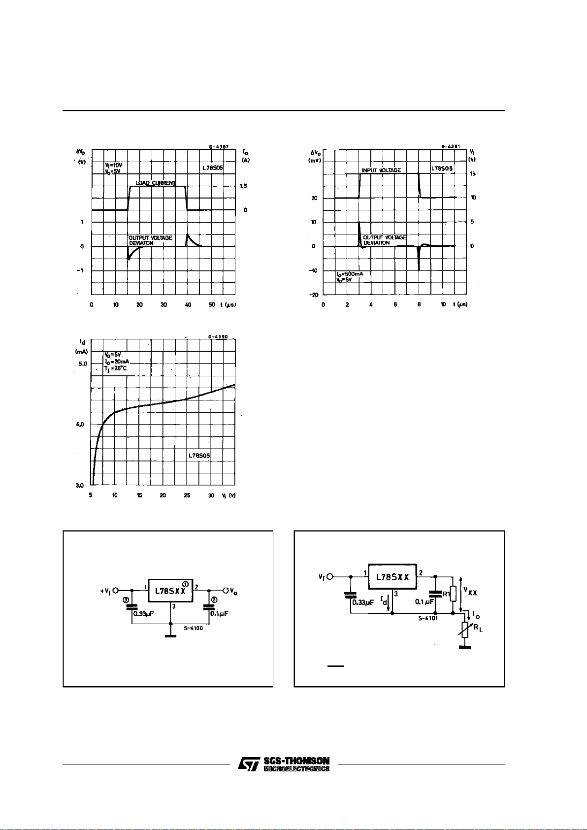
Figure 12 : QuiescentCurrent vs. Input Voltage.
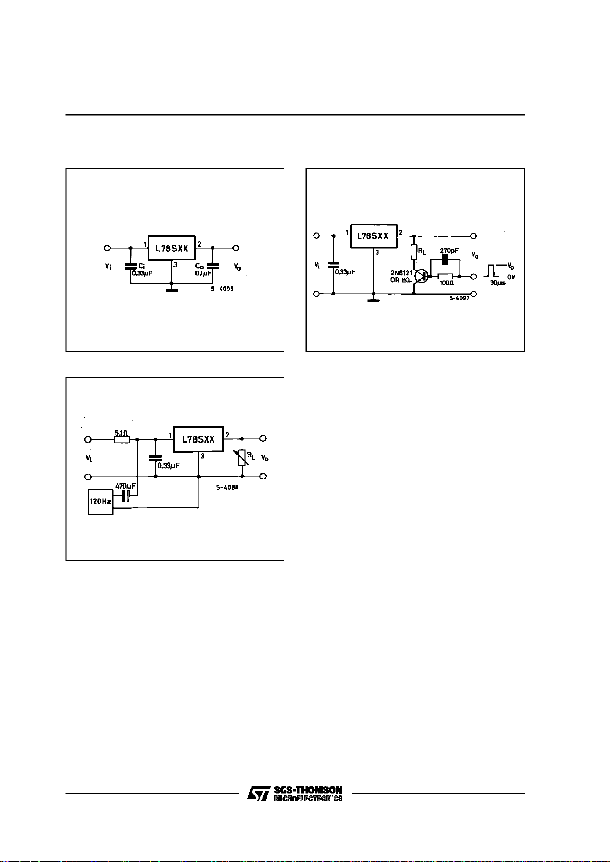
Figure 13 : Fixed OutputRegulator. Figure 14 : Constant Current Regulator.
Figure 10 : Load Transient Response. Figure 11 : Line TransientResponse.
Notes : 1. To specify an output voltage, substitute voltage
value for ”XX”.
2. Although no output capacitor is needed for stability, it does improve transient response.
3. Required if regulator is located an appreciable
dis-tance from power supply filter.
V
XX
IO=+I
d
R
1
L78S00 SERIES
14/21
Figure15 : Circuitfor Increasing Output Voltage. Figure 16 : Adjustable Output Regulator
(7 to 30V).
Figure 17 : 0.5 to 10V Regulator. Figure 18 : High Current Voltage Regulator.
V
BEQ
1
R1=
I
Q
1
I
REQ
–
β
Q
1
V
BEQ
1
IO=I
REG
+Q1[I
REG
–]
R
1
R
4
V
O=VXX
R
1
IR1≥ 5I
d
R
2
V0=VXX(1 + ) + IdR
2
R
1
Figure 19 : High Output Current with Short Circuit
Protection.
Figure 20 : TrackingVoltage Regulator.
V
BEQ
2
RSC=
I
SC
L78S00 SERIES
15/21
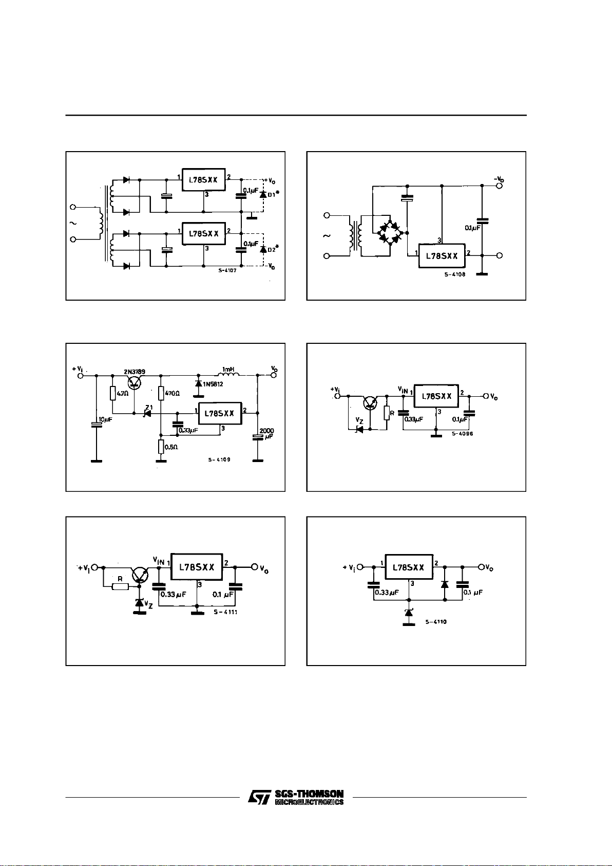
Figure 21 : Positiveand NegativeRegulator. Figure 22 : Negative Output Voltage Circuit.
Figure 23 : Switching Regulator. Figure 24 : High Input Voltage Circuit.
VIN=Vi–(VZ+VBE)
(*) D1and D2are necessary if the load is connected between + V0and – V0.
Figure 25 : High Input Voltage Circuit. Figure 26 : High Output VoltageRegulator.
VIN=VZ-V
BE
L78S00 SERIES
16/21
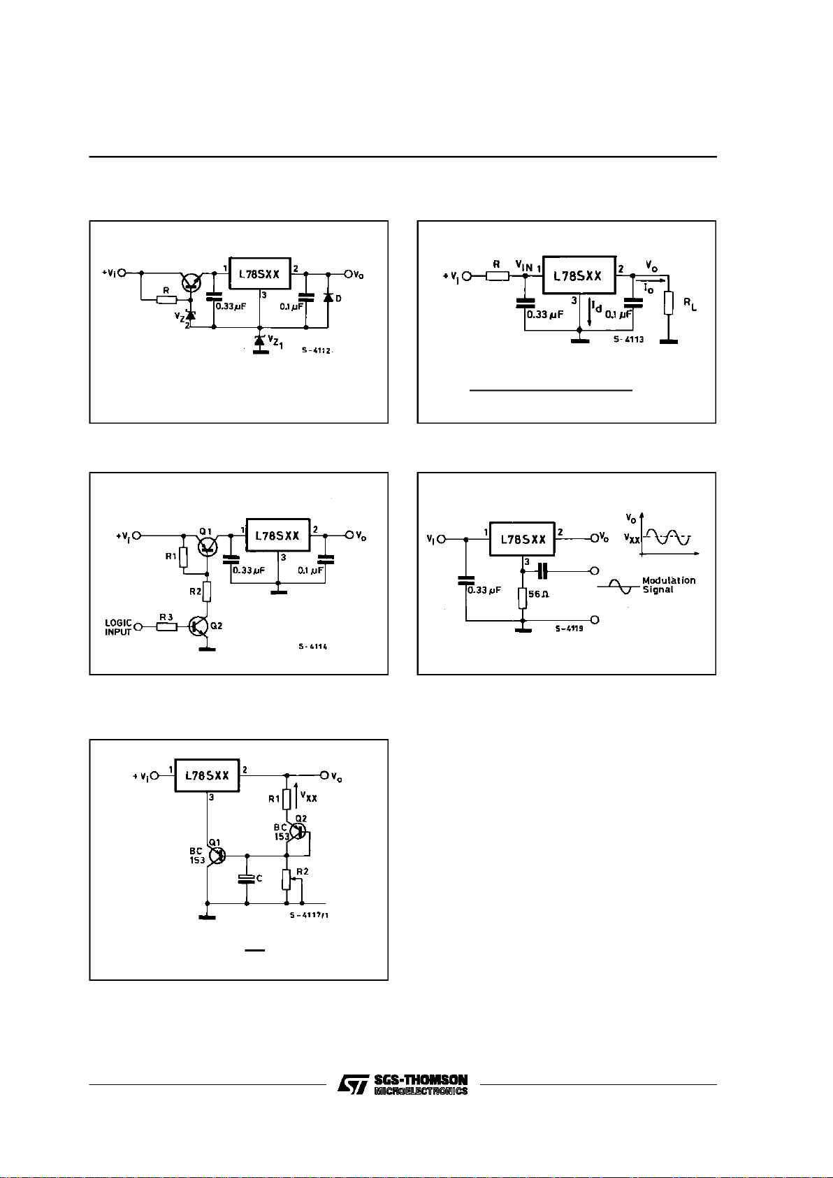
Figure 27 : High Input and Output Voltage. Figure 28 : Reducing Power Dissipation with
Dropping Resistor.
VO=VXX+V
Z1
V
i(min)–VXX–VDROP(max)
R=
I
O(max)+Id(max)
Figure 29 : Remote Shuntdown. Figure 30 : Power AM Modulator (unity voltage
gain,Io ≤ 1A).
Note : The circuit performs well up to 100KHz.
Figure 31 : AdjustableOutput Voltage with Tem-
peratureCompensation.
Note :Q2is conn ec ted as a diode in order to compensate
the variation of the Q1VBEwit h the tem perature. C
allows a slow rise-time of the V
O
R
2
VO=VXX(1+ ) + V
BE
R
1
L78S00 SERIES
17/21
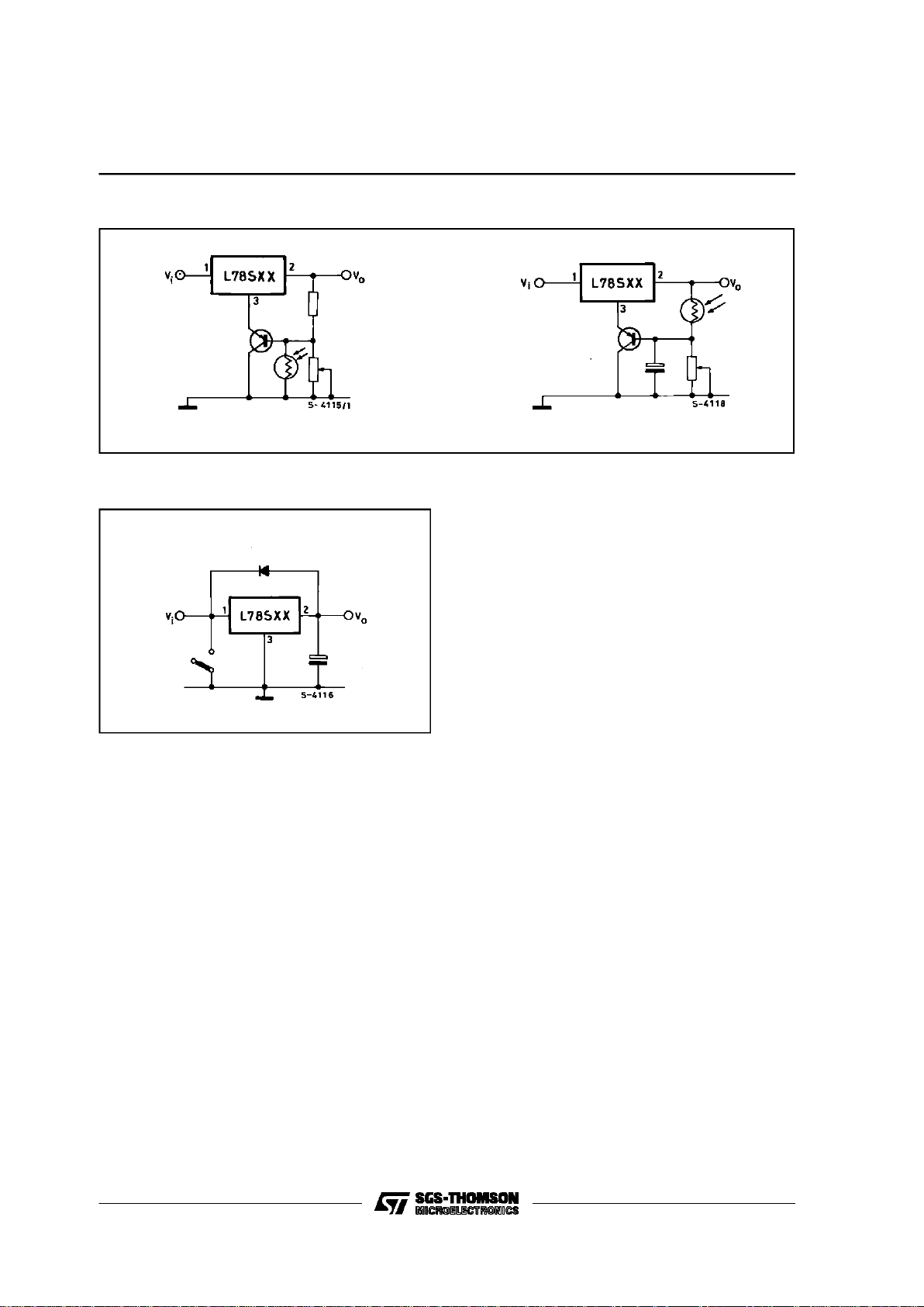
Figure 32 : Light Controllers (V
o min=Vxx+VBE
).
VOfalls when the lightgoes up VOrises when the light goes up
Figure 33 : Protectionagainst Input Short-circuit
withHigh Capacitance Loads.
Applications with high capacitance loads and an
outputvoltage greater than 6 volts needan external
diode(see fig.33)to protect the deviceagainst input
short circuit. In this case the input voltage falls
rapidly while the output voltage decreases showly.
The capacitancedischarges by means of the BaseEmitter junction of the series pass transistor in the
regulator. If the energy is sufficientlyhigh, the transistor may be destroyed. The external diode bypasses thecurrent from the IC to ground.
L78S00 SERIES
18/21

DIM.
mm inch
MIN. TYP. MAX. MIN. TYP. MAX.
A 11.00 13.10 0.433 0.516
B 0.97 1.15 0.038 0.045
C 1.50 1.65 0.059 0.065
D 8.32 8.92 0.327 0.351
E 19.00 20.00 0.748 0.787
G 10.70 11.10 0.421 0.437
N 16.50 17.20 0.649 0.677
P 25.00 26.00 0.984 1.023
R 4.00 4.09 0.157 0.161
U 38.50 39.30 1.515 1.547
V 30.00 30.30 1.187 1.193
C
D
N
B
V
U
R
A
P
E
G
O
P003F
TO-3 MECHANICAL DATA
L78S00 SERIES
19/21

DIM.
mm inch
MIN. TYP. MAX. MIN. TYP. MAX.
A 4.40 4.60 0.173 0.181
C 1.23 1.32 0.048 0.051
D 2.40 2.72 0.094 0.107
D1 1.27 0.050
E 0.49 0.70 0.019 0.027
F 0.61 0.88 0.024 0.034
F1 1.14 1.70 0.044 0.067
F2 1.14 1.70 0.044 0.067
G 4.95 5.15 0.194 0.203
G1 2.4 2.7 0.094 0.106
H2 10.0 10.40 0.393 0.409
L2 16.4 0.645
L4 13.0 14.0 0.511 0.551
L5 2.65 2.95 0.104 0.116
L6 15.2 15.9 0.598 0.625
L7 6.2 6.6 0.244 0.260
L9 3.5 4.2 0.137 0.165
DIA. 3.75 3.85 0.147 0.151
L6
A
C
D
E
D1
F
G
L7
L2
Dia.
F1
L5
L4
H2
L9
F2
G1
TO-220 MECHANICAL DATA
P011C
L78S00 SERIES
20/21

Information furnished is believed to be accurate and reliable.However, SGS-THOMSON Microelectronics assumes no responsability for the
consequences of use of such information nor for any infringementof patents or other rights of third parties which may results from its use. No
license isgranted by implication or otherwise underany patent or patentrights of SGS-THOMSON Microelectronics. Specificationsmentioned
in this publication are subject to changewithout notice. This publication supersedes and replaces all information previously supplied.
SGS-THOMSON Microelectronicsproductsare notauthorizedforuse ascritical componentsinlife supportdevices orsystems withoutexpress
written approval of SGS-THOMSON Microelectonics.
1994 SGS-THOMSON Microelectronics - All RightsReserved
SGS-THOMSON MicroelectronicsGROUP OF COMPANIES
Australia - Brazil - France - Germany - Hong Kong - Italy - Japan - Korea - Malaysia - Malta - Morocco - The Netherlands -
Singapore - Spain - Sweden - Switzerland - Taiwan - Thailand - United Kingdom - U.S.A
L78S00 SERIES
21/21
 Loading...