

SGS Thomson Microelectronics L78M18CDT-1, L78M15CDT-1, L78M24CDT-1, L78M06CDT-1, L78M10CDT-1 Datasheet
...
1/21February 2003
■ OUTPUT CURRENT TO 0.5A
■ OUTPUT VOLTAGES OF 5; 6; 8; 9; 12; 15;
18; 20; 24V
■ THERMAL OVERLOAD PROTECTION
■ SHORT CIRCUIT PROTECTION
■ OUTPUT TRANSITION SOA PROTECTION
DESCRIPTION
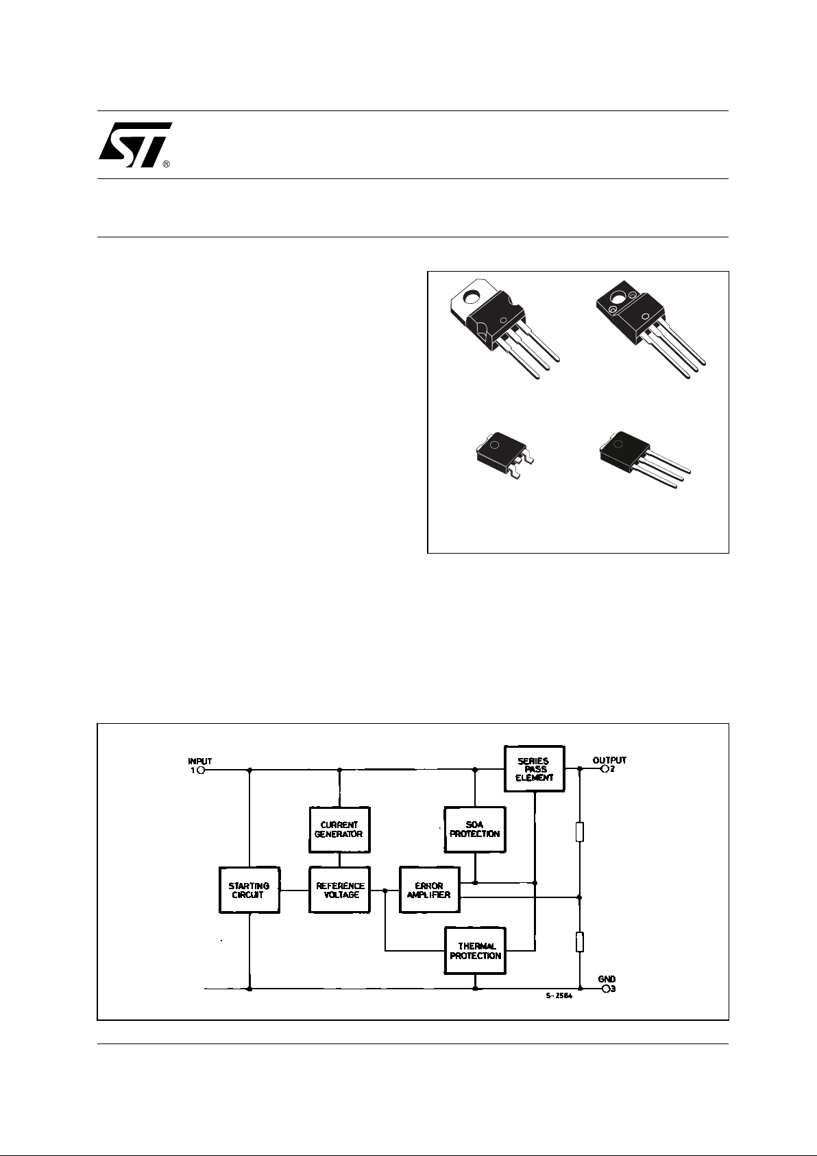
The L78M00 series of three-terminal positive
regulators is available in TO-220, TO-220FP,
DPAK and IPAK packag es and with several fixed
output voltages,making it u se ful in a wide range of
applications. These regulators can provide local
on-card regulation, eliminating the distribution
problems associated with single point regulation.
Each type employs int ernal current limiting,
thermal shut-down and safe area protection,
making it essentially indestructible . If adequate
heat sin king is prov ided, they can deliver over
0.5A output current. Althoug h designed primarily
as fixed voltage regulators, these devices can be
used with external components to obtain
adjustable voltage and currents.
L78M00
SERIES
POSITIVE VOLTAGE REGULATORS
SCHEMATIC DIAGRAM
TO-220
DPAK
TO-220FP
IPAK
L78M00 SE RIES
2/21
ABSOLUTE MAXIMUM RATINGS
Absolute Maximum Ratings are those values beyond which damage to the device may occur. Functional operation under these condition is
not implied.
THERMAL DATA
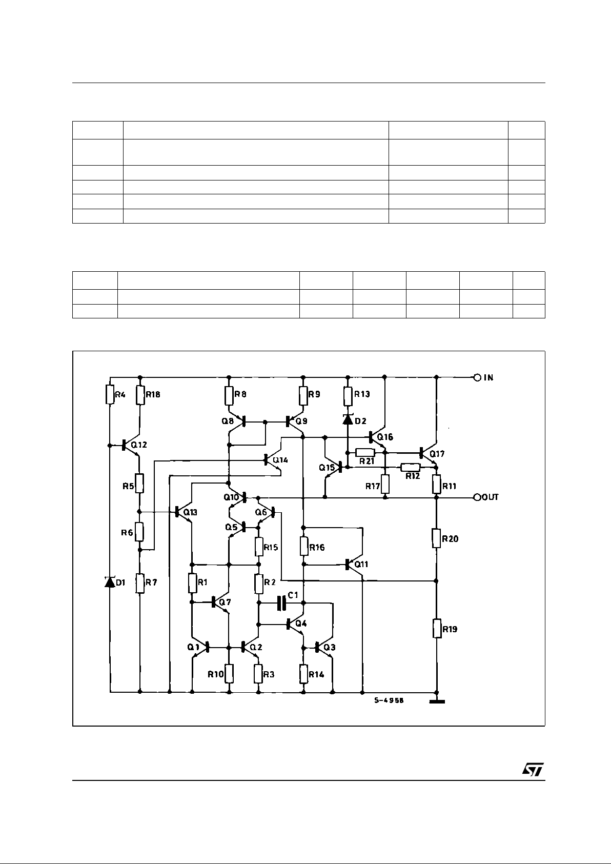
SHEMATIC DIAGRAM
Symbol Parameter² Value Unit
V
I
DC Input Voltage (for VO= 5 to 18V)
(for V
O
= 20, 24V)
35
40
V
V
I
O
Output Current
Internally Limited mA
P
D
Power Dissipation
Internally Limited mW
T
stg
Storage Temperature Range
-65 to +150 °C
T
op
Operating Junction Temperature Range
0 to +150 °C
Symbol Parameter TO-220 TO-220FP DPAK IPAK Unit
R
thj-case
Thermal Resistance Junction-case
3 5 8 °C/W
R
thj-amb
Thermal Resistance Junction-ambient
50 60 100 °C/W
L78M00 SE RIES
3/21
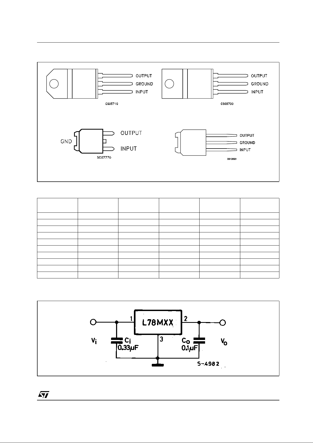
CONNECTION DIAGRAM (t op v iew)
ORDERING CODES
(*) Available in Tape & Reel with the suffix "-TR".
APPLICATION CIRCUITS
TYPE TO-220 TO-220FP DPAK (*) IPAK
OUTPUT
VOLTAGE
L78M05 L78M05CV L78M05CP L78M05CDT L78M05CDT-1 5 V
L78M06 L78M06CV L78M06CP L78M06CDT L78M06CDT-1 6 V
L78M08 L78M08CV L78M08CP L78M08CDT L78M08CDT-1 8 V
L78M09 L78M09CV L78M09CP L78M09CDT L78M09CDT-1 9 V
L78M10 L78M10CV L78M10CP L78M10CDT L78M10CDT-1 10 V
L78M12 L78M12CV L78M12CP L78M12CDT L78M12CDT-1 12 V
L78M15 L78M15CV L78M15CP L78M15CDT L78M15CDT-1 15 V
L78M18 L78M18CV L78M18CP L78M18CDT L78M18CDT-1 18 V
L78M20 L78M20CV L78M20CP L78M20CDT L78M20CDT-1 20 V
L78M24 L78M24CV L78M24CP L78M24CDT L78M24CDT-1 24 V
TO-220 TO-220FP
IPAK
DPAK
L78M00 SE RIES
4/21
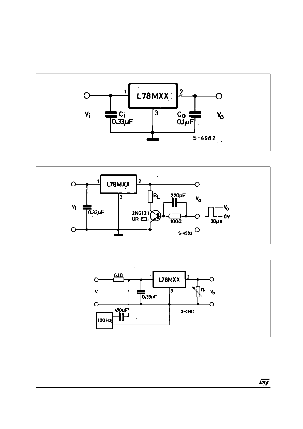
TEST CIRCUITS
Figure1 : DC Parameter
Figure2 : Load Regulation
Figure3 : Ripple Rejection
L78M00 SE RIES
5/21
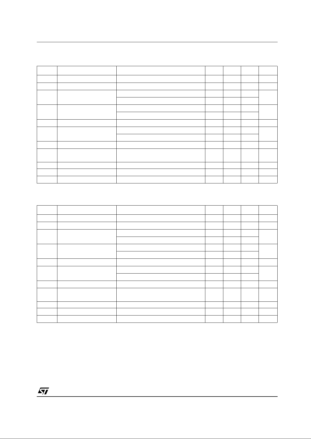
ELECTRICAL CHARACTERISTICS OF L78M05C (refer to the test circuits, TJ= 25°C, VI=10V,
I
O
=350mA,CI=0.33µF,CO= 0.1 µF unless otherwise specified).
ELECTRICAL CHARACTERISTICS OF L78M06C (refer to the test circuits, T
J
= 25°C, VI=11V,
I
O
=350mA,CI=0.33µF,CO= 0.1 µF unless otherwise specified).
Symbol Parameter Test Conditions Min. Typ. Max. Unit
V
O
Output Voltage 4.8 5 5.2 V
V
O
Output Voltage IO= 5 to 350 mA VI= 7 to 20 V 4.75 5 5.25 V
∆V
O
Line Regulation VI=7to25V IO= 200 mA 100 mV
V
I
=8to25V IO= 200 mA 50
∆V
O
Load Regulation IO= 5 to 500 mA TJ= 25°C 100 mV
I
O
= 5 to 200 mA TJ= 25°C 50
I
d
Quiescent Current 6mA
∆I
d
Quiescent Current Change IO= 5 to 350 mA 0.5 mA
I
O
= 200 mA VI= 8 to 25 V 0.8
∆V
O
/∆T Output Voltage Drift IO=5mA TJ= 0 to 125°C -0.5 mV/°C
SVR Supply Voltage Rejection V
I
= 8 to 18 V f = 120Hz
I
O
= 300mA
62 dB
eN Output Noise Voltage B =10Hz to 100KHz 40 µV
V
d
Dropout Voltage 2 V
I
sc
Short Circuit Current VI= 35 V 300 mA
Symbol Parameter Test Conditions Min. Typ. Max. Unit
V
O
Output Voltage 5.75 6 6.25 V
V
O
Output Voltage IO= 5 to 350 mA VI= 8 to 21 V 5.7 6 6.3 V
∆V
O
Line Regulation VI=8to25V IO= 200 mA 100 mV
V
I
=9to25V IO= 200 mA 50
∆V
O
Load Regulation IO= 5 to 500 mA TJ= 25°C 120 mV
I
O
= 5 to 200 mA TJ= 25°C 60
I
d
Quiescent Current 6mA
∆I
d
Quiescent Current Change IO= 5 to 350 mA 0.5 mA
I
O
= 200 mA VI= 9 to 25 V 0.8
∆V
O
/∆T Output Voltage Drift IO=5mA TJ= 0 to 125°C -0.5 mV/°C
SVR Supply Voltage Rejection V
I
= 9 to 19 V f = 120Hz
I
O
= 300mA
59 dB
eN Output Noise Voltage B =10Hz to 100KHz 45 µV
V
d
Dropout Voltage 2 V
I
sc
Short Circuit Current VI= 35 V 270 mA
L78M00 SE RIES
6/21
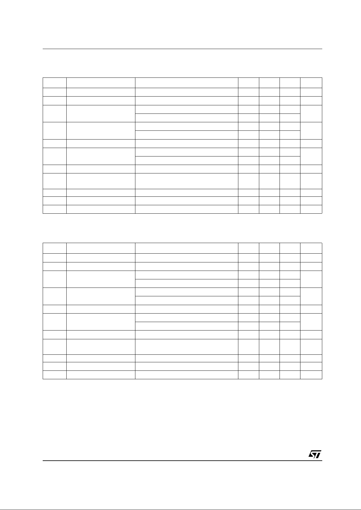
ELECTRICAL CHARACTERISTICS OF L78M08C (refer to the test circuits, TJ= 25°C, VI=14V,
I
O
=350mA,CI=0.33µF,CO= 0.1 µF unless otherwise specified).
ELECTRICAL CHARACTERISTICS OF L78M09C (refer to the test circuits, T
J
= 25°C, VI=15V,
I
O
=350mA,CI=0.33µF,CO= 0.1 µF unless otherwise specified).
Symbol Parameter Test Conditions Min. Typ. Max. Unit
V
O
Output Voltage 7.7 8 8.3 V
V
O
Output Voltage IO= 5 to 350 mA VI= 10.5 to 23 V 7.6 8 8.4 V
∆V
O
Line Regulation VI= 10.5 to 25 V IO= 200 mA 100 mV
V
I
=11to25V IO= 200 mA 50
∆V
O
Load Regulation IO= 5 to 500 mA TJ= 25°C 160 mV
I
O
= 5 to 200 mA TJ= 25°C 80
I
d
Quiescent Current 6mA
∆I
d
Quiescent Current Change IO= 5 to 350 mA 0.5 mA
I
O
= 200 mA VI= 10.5 to 25 V 0.8
∆V
O
/∆T Output Voltage Drift IO=5mA TJ= 0 to 125°C -0.5 mV/°C
SVR Supply Voltage Rejection V
I
= 11.5 to 21.5 V f = 120Hz
I
O
= 300mA
56 dB
eN Output Noise Voltage B =10Hz to 100KHz 52 µV
V
d
Dropout Voltage 2 V
I
sc
Short Circuit Current VI= 35 V 250 mA
Symbol Parameter Test Conditions Min. Typ. Max. Unit
V
O
Output Voltage 8.65 9 9.35 V
V
O
Output Voltage IO= 5 to 350 mA VI= 11.5 to 24 V 8.55 9 9.45 V
∆V
O
Line Regulation VI= 11.5 to 25 V IO= 200 mA 100 mV
V
I
=12to25V IO= 200 mA 50
∆V
O
Load Regulation IO= 5 to 500 mA TJ= 25°C 180 mV
I
O
= 5 to 200 mA TJ= 25°C 90
I
d
Quiescent Current 6mA
∆I
d
Quiescent Current Change IO= 5 to 350 mA 0.5 mA
I
O
= 200 mA VI= 11.5 to 25 V 0.8
∆V
O
/∆T Output Voltage Drift IO=5mA TJ= 0 to 125°C -0.5 mV/°C
SVR Supply Voltage Rejection V
I
= 12.5 to 23 V f = 120Hz
I
O
= 300mA
56 dB
eN Output Noise Voltage B =10Hz to 100KHz 58 µV
V
d
Dropout Voltage 2 V
I
sc
Short Circuit Current VI= 35 V 250 mA

L78M00 SE RIES
7/21
ELECTRICAL CHARACTERISTICS OF L78M10C (refer to the test circuits, TJ= 25°C, VI=16V,
I
O
=350mA,CI=0.33µF,CO= 0.1 µF unless otherwise specified).
ELECTRICAL CHARACTERISTICS OF L78M12C (refer to the test circuits, T
J
= 25°C, VI=19V,
I
O
=350mA,CI=0.33µF,CO= 0.1 µF unless otherwise specified).
Symbol Parameter Test Conditions Min. Typ. Max. Unit
V
O
Output Voltage 9.6 10 10.4 V
V
O
Output Voltage IO= 5 to 350 mA VI= 12.5 to 25 V 9.5 10 10.5 V
∆V
O
Line Regulation VI= 12.5 to 30 V IO= 200 mA 100 mV
V
I
=13to30V IO= 200 mA 50
∆V
O
Load Regulation IO= 5 to 500 mA TJ= 25°C 200 mV
I
O
= 5 to 200 mA TJ= 25°C 100
I
d
Quiescent Current 6mA
∆I
d
Quiescent Current Change IO= 5 to 350 mA 0.5 mA
I
O
= 200 mA VI= 12.5 to 30 V 0.8
∆V
O
/∆T Output Voltage Drift IO=5mA TJ= 0 to 125°C -0.5 mV/°C
SVR Supply Voltage Rejection V
I
= 13.5 to 24 V f = 120Hz
I
O
= 300mA
56 dB
eN Output Noise Voltage B =10Hz to 100KHz 64 µV
V
d
Dropout Voltage 2 V
I
sc
Short Circuit Current VI= 35 V 245 mA
Symbol Parameter Test Conditions Min. Typ. Max. Unit
V
O
Output Voltage 11.5 12 12.5 V
V
O
Output Voltage IO= 5 to 350 mA VI= 14.5 to 27 V 11.4 12 12.6 V
∆V
O
Line Regulation VI= 14.5 to 30 V IO= 200 mA 100 mV
V
I
=16to30V IO= 200 mA 50
∆V
O
Load Regulation IO= 5 to 500 mA TJ= 25°C 240 mV
I
O
= 5 to 200 mA TJ= 25°C 120
I
d
Quiescent Current 6mA
∆I
d
Quiescent Current Change IO= 5 to 350 mA 0.5 mA
I
O
= 200 mA VI= 14.5 to 30 V 0.8
∆V
O
/∆T Output Voltage Drift IO=5mA TJ= 0 to 125°C -1 mV/°C
SVR Supply Voltage Rejection V
I
= 15 to 25 V f = 120Hz
I
O
= 300mA
55 dB
eN Output Noise Voltage B =10Hz to 100KHz 75 µV
V
d
Dropout Voltage 2 V
I
sc
Short Circuit Current VI= 35 V 240 mA

L78M00 SE RIES
8/21
ELECTRICAL CHARACTERISTICS OF L78M15C (refer to the test circuits, TJ= 25°C, VI=23V,
I
O
=350mA,CI=0.33µF,CO= 0.1 µF unless otherwise specified).
ELECTRICAL CHARACTERISTICS OF L78M18C (refer to the test circuits, T
J
= 25°C, VI=26V,
I
O
=350mA,CI=0.33µF,CO= 0.1 µF unless otherwise specified).
Symbol Parameter Test Conditions Min. Typ. Max. Unit
V
O
Output Voltage 14.4 15 15.6 V
V
O
Output Voltage IO= 5 to 350 mA VI= 17.5 to 30 V 14.25 15 15.75 V
∆V
O
Line Regulation VI= 17.5 to 30 V IO= 200 mA 100 mV
V
I
=20to30V IO= 200 mA 50
∆V
O
Load Regulation IO= 5 to 500 mA TJ= 25°C 300 mV
I
O
= 5 to 200 mA TJ= 25°C 150
I
d
Quiescent Current 6mA
∆I
d
Quiescent Current Change IO= 5 to 350 mA 0.5 mA
I
O
= 200 mA VI= 17.5 to 30 V 0.8
∆V
O
/∆T Output Voltage Drift IO=5mA TJ= 0 to 125°C -1 mV/°C
SVR Supply Voltage Rejection V
I
= 18.5 to 28.5 V f = 120Hz
I
O
= 300mA
54 dB
eN Output Noise Voltage B =10Hz to 100KHz 90 µV
V
d
Dropout Voltage 2 V
I
sc
Short Circuit Current VI= 35 V 240 mA
Symbol Parameter Test Conditions Min. Typ. Max. Unit
V
O
Output Voltage 17.3 18 18.7 V
V
O
Output Voltage IO= 5 to 350 mA VI= 20.5 to 33 V 17.1 18 18.9 V
∆V
O
Line Regulation VI=21to33V IO= 200 mA 100 mV
V
I
=24to33V IO= 200 mA 50
∆V
O
Load Regulation IO= 5 to 500 mA TJ= 25°C 360 mV
I
O
= 5 to 200 mA TJ= 25°C 180
I
d
Quiescent Current 6mA
∆I
d
Quiescent Current Change IO= 5 to 350 mA 0.5 mA
I
O
= 200 mA VI=21to33V 0.8
∆V
O
/∆T Output Voltage Drift IO=5mA TJ= 0 to 125°C -1.1 mV/°C
SVR Supply Voltage Rejection V
I
= 22 to 32 V f = 120Hz
I
O
= 300mA
53 dB
eN Output Noise Voltage B =10Hz to 100KHz 100 µV
V
d
Dropout Voltage 2 V
I
sc
Short Circuit Current VI= 35 V 240 mA

L78M00 SE RIES
9/21
ELECTRICAL CHARACTERISTICS OF L78M20C (refer to the test circuits, TJ= 25°C, VI=29V,
I
O
=350mA,CI=0.33µF,CO= 0.1 µF unless otherwise specified).
ELECTRICAL CHARACTERISTICS OF L78M24C (refer to the test circuits, T
J
= 25°C, VI=33V,
I
O
=350mA,CI=0.33µF,CO= 0.1 µF unless otherwise specified),
Symbol Parameter Test Conditions Min. Typ. Max. Unit
V
O
Output Voltage 19.2 20 20.8 V
V
O
Output Voltage IO= 5 to 350 mA VI=23to35V 19 20 21 V
∆V
O
Line Regulation VI=23to35V IO= 200 mA 100 mV
V
I
=24to35V IO= 200 mA 50
∆V
O
Load Regulation IO= 5 to 500 mA TJ= 25°C 400 mV
I
O
= 5 to 200 mA TJ= 25°C 200
I
d
Quiescent Current 6mA
∆I
d
Quiescent Current Change IO= 5 to 350 mA 0.5 mA
I
O
= 200 mA VI=23to35V 0.8
∆V
O
/∆T Output Voltage Drift IO=5mA TJ= 0 to 125°C -1.1 mV/°C
SVR Supply Voltage Rejection V
I
= 24 to 34 V f = 120Hz
I
O
= 300mA
53 dB
eN Output Noise Voltage B =10Hz to 100KHz 110 µV
V
d
Dropout Voltage 2 V
I
sc
Short Circuit Current VI= 35 V 240 mA
Symbol Parameter Test Conditions Min. Typ. Max. Unit
V
O
Output Voltage 23 24 25 V
V
O
Output Voltage IO= 5 to 350 mA VI=27to38V 22.8 24 25.2 V
∆V
O
Line Regulation VI=27to38V IO= 200 mA 100 mV
V
I
=28to38V IO= 200 mA 50
∆V
O
Load Regulation IO= 5 to 500 mA TJ= 25°C 480 mV
I
O
= 5 to 200 mA TJ= 25°C 240
I
d
Quiescent Current 6mA
∆I
d
Quiescent Current Change IO= 5 to 350 mA 0.5 mA
I
O
= 200 mA VI=27to38V 0.8
∆V
O
/∆T Output Voltage Drift IO=5mA TJ= 0 to 125°C -1.2 mV/°C
SVR Supply Voltage Rejection V
I
= 28 to 38 V f = 120Hz
I
O
= 300mA
50 dB
eN Output Noise Voltage B =10Hz to 100KHz 170 µV
V
d
Dropout Voltage 2 V
I
sc
Short Circuit Current VI= 35 V 240 mA

L78M00 SE RIES
10/21
Figure4 : Dropout Voltage vs Junction
Temperature
Figure5 : Dropout Characteristics
Figure6 : Peak Output Current vs Input-Output
Differential Voltage
Figure7 : Output Voltage vs Junction
Temperature
Figure8 : Supply Voltage Rejection vs
Frequency
Figure9 : Quiescent Current vs Junction
Temperature

L78M00 SE RIES
11/21
Figure10 : Load Transient Response
Figure11 : Line Transient Response
Figure12 : Quiescent Current vs Input Voltage

L78M00 SE RIES
12/21
Figure13 : Fixed Output Regulator
NOTE:
1. To specify an output voltage, substitute voltage value for "XX".
2. Although no output capacitor is need for stability, it does improve transient response.
3. Required if regulator is locate an appreciable distance from power supply filter.
Figure14 :
Figure15 :
V
xx
IO= +I
d
R
1
IR1≥ 5Id
R
2
VO=VXX(1+ )+IdR
2
R
1

L78M00 SE RIES
13/21
Figure16 : Adjustable Output Regulator (7 to 30V)
Figure17 : 0.5 to 10V Regulator
Figure18 : High Current Voltage Regulator
Figure19 : High Output Current with Short Circuit
R
4
VO=Vxx
R
1
V
BEQ1
R1=
I
Q1
I
REQ
-
β
Q1
V
BEQ1
IO=I
REG+Q1(IREG
)
R
1
V
BEQ2
VO=
I
SC

L78M00 SE RIES
14/21
Figure20 : Tracking Voltage Regulator
Figure21 : High Input Voltage Circuit
Figure22 : Reducing Power Dissipation with Dropping Resistor
VIN=VI-(VZ+VBE)
V
I(min) -VXX -VDROP(max)
R=
I
O(max) +Id(max)

L78M00 SE RIES
15/21
Figure23 : Power AM Modulator (unity voltage gain, I
O
≤ 0.5)
NOTE: The circuit performs well up to 100 KHz.
Figure24 : Adjustable Output Voltage with Temperature Com pensation
NOTE:Q2is connected as a diode inorder tocompensatethe variation of theQ1VBEwith the temperature. C allows aslowrisetime of theVO.
R
2
VO=VXX(1+ ) +V
BE
R
1

L78M00 SE RIES
16/21
DIM.
mm. inch
MIN. TYP MAX. MIN. TYP. MAX.
A 4.40 4.60 0.173 0.181
C 1.23 1.32 0.048 0.051
D 2.40 2.72 0.094 0.107
D1 1.27 0.050
E 0.49 0.70 0.019 0.027
F 0.61 0.88 0.024 0.034
F1 1.14 1.70 0.044 0.067
F2 1.14 1.70 0.044 0.067
G 4.95 5.15 0.194 0.203
G1 2.4 2.7 0.094 0.106
H2 10.0 10.40 0.393 0.409
L2 16.4 0.645
L4 13.0 14.0 0.511 0.551
L5 2.65 2.95 0.104 0.116
L6 15.25 15.75 0.600 0.620
L7 6.2 6.6 0.244 0.260
L9 3.5 3.93 0.137 0.154
DIA. 3.75 3.85 0.147 0.151
TO-220 MECHANICAL DAT
A
P011C

L78M00 SE RIES
17/21
DIM.
mm. inch
MIN. TYP MAX. MIN. TYP. MAX.
A 4.40 4.60 0.173 0.181
B 2.5 2.7 0.098 0.106
D 2.5 2.75 0.098 0.108
E 0.45 0.70 0.017 0.027
F 0.75 1 0.030 0.039
F1 1.15 1.50 0.045 0.059
F2 1.15 1.50 0.045 0.059
G 4.95 5.2 0.194 0.204
G1 2.4 2.7 0.094 0.106
H 10.0 10.40 0.393 0.409
L2 16 0.630
L3 28.6 30.6 1.126 1.204
L4 9.8 10.6 0.385 0.417
L6 15.9 16.4 0.626 0.645
L7 9 9.3 0.354 0.366
DIA. 3 3.2 0.118 0.126
TO-220FP MECHANICAL DATA
L2
A
B
D
E
H
G
L6
¯
F
L3
G1
123
F2
F1
L7
L4
7012510/F

L78M00 SE RIES
18/21
DIM.
mm. inch
MIN. TYP MAX. MIN. TYP. MAX.
A 2.2 2.4 0.086 0.094
A1 0.9 1.1 0.035 0.043
A2 0.03 0.23 0.001 0.009
B 0.64 0.9 0.025 0.035
B2 5.2 5.4 0.204 0.212
C 0.45 0.6 0.017 0.023
C2 0.48 0.6 0.019 0.023
D 6 6.2 0.236 0.244
E 6.4 6.6 0.252 0.260
G 4.4 4.6 0.173 0.181
H 9.35 10.1 0.368 0.397
L2 0.8 0.031
L4 0.6 1 0.023 0.039
DPAK MECHANI
CAL DATA
0068772-B

L78M00 SE RIES
19/21
DIM.
mm. inch
MIN. TYP MAX. MIN. TYP. MAX.
A 2.2 2.4 0.086 0.094
A1 0.9 1.1 0.035 0.043
B 0.64 0.9 0.025 0.035
B2 5.2 5.4 0.204 0.212
B3 0.95 0.037
B5 0.3 0.012
B6 0.95 0.037
C 0.45 0.6 0.017 0.023
C2 0.48 0.6 0.019 0.023
D 6 6.2 0.236 0.244
E 6.4 6.6 0.252 0.260
G 4.4 4.6 0.173 0.181
H 15.9 16.3 0.626 0.641
L 9 9.4 0.354 0.370
L1 0.8 1.2 0.031 0.047
L2 0.8 1 0.031 0.039
IPAK MECHANICAL DATA
0068771-F

L78M00 SE RIES
20/21
DIM.
mm. inch
MIN. TYP MAX. MIN. TYP. MAX.
A 180 7.086
C 12.8 13.0 13.2 0.504 0.512 0.519
D 20.2 0.795
N 60 2.362
T 14.4 0.567
Ao 6.80 6.90 7.00 0.268 0.272 0.2.76
Bo 10.40 10.50 10.60 0.409 0.413 0.417
Ko 2.55 2.65 2.75 0.100 0.104 0.105
Po 3.9 4.0 4.1 0.153 0.157 0.161
P 7.9 8.0 8.1 0.311 0.315 0.319
Tape & Reel DPAK-PPAK MECHANICAL DATA

L78M00 SE RIES
21/21
Information furnished is believed to be accurate and reliable. However, STMicroelectronics assumes no responsibility for the
consequences of use o f suc h inf ormat ion n or f or an y infr ingeme nt of paten ts or oth er ri gh ts of third part ies whic h may resul t f rom
its use. No license is granted by implication or otherwise under any patent or patent rights of STMicroelectronics. Specifications
mentioned in this publication are subject to change without notice. This publication supersedes and replaces all information
previously supplied. STMicroelectronics products are not authorized for use as critical components in life support devices or
systems without express written approval of STMicroelectronics.
© The ST logo is a registered trademark of STMicroelectronics
© 2003 STMicroelectronics - Printed in Italy - All Rights Reserved
STMicroelectronics GROUP OF COMPANIES
Australia - Brazil - Canada - China - Finland - France - Germany - Hong Kong - India - Israel - Italy - Japan - Malaysia - Malta - Morocco
Singapore - Spain - Sweden - Switzerland - United Kingdom - United States.
© http://www.st.com
 Loading...