

Datasheet L78M20CV, L78M20CS, L78M12CV, L78M12CS, L78M12CP Datasheet (SGS Thomson Microelectronics)
...
L78M00
SERIES
POSITIVE VOLTAGE REGULATORS
September 1998
■ OUTPUTCURRENT TO0.5A
■ OUTPUTVOLTAGESOF 5; 6; 8; 9; 10; 12;15;
18; 20; 24V
■ THERMAL OVERLOADPROTECTION
■ SHORTCIRCUIT PROTECTION
■ OUTPUTTRANSISTOR SOAPROTECTION
DESCRIPTION
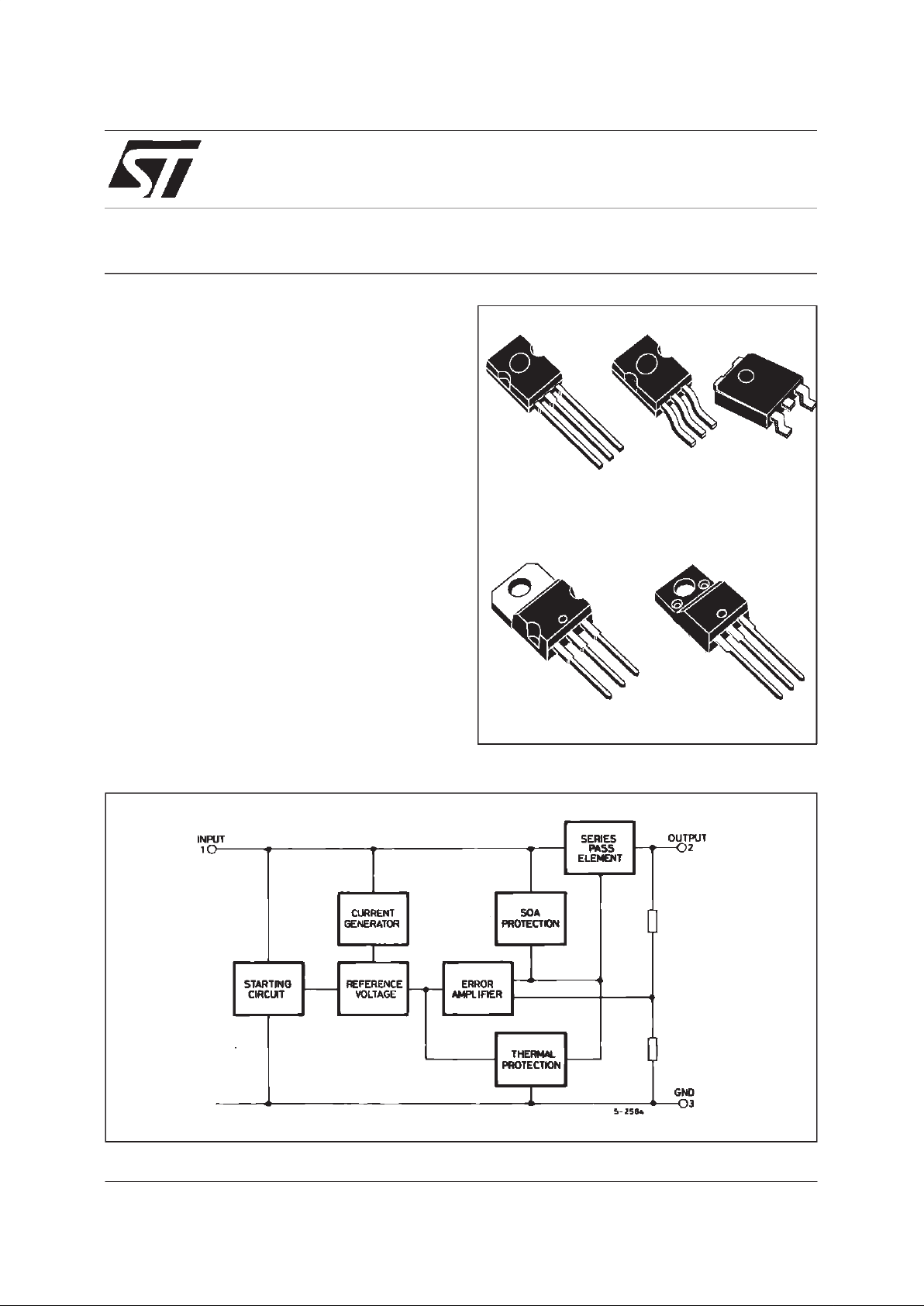
The L78M00 series of three-terminal positive
regulators is available in TO-220, ISOWATT220,
SOT-82, SOT-194 and DPAK packages and with
several fixed output voltages, making it useful in
a wide range of applications. These regulators
can provide local on-card regulation, eliminating
the distribution problems associated with single
point regulation. Each type employs internal
current limiting, thermal shut-down and safe area
protection, making it essentially indestructible. If
adequate heat sinking is provided, they can
deliver over 0.5A output current. Although
designed primarily as fixed voltage regulators,
these devices can be used with external
components to obtain adjustable voltages and
currents.
TO-220 ISOWATT220
BLOCK DIAGRAM
SOT-82 SOT-194 DPAK
1/19
ABSOLUTE MAXIMUM RATINGS
Symbol Parameter Value Unit
V
i
DC InputVoltage(forVO=5to18V)
(forV
O
= 20,24V)
35
40
V
V
I
o
OutputCurrent Internally limited
P
tot
Power Dissipation Internally limited
T
op
Operating Junction Temperature Range 0 to 150
o
C
T
stg
StorageTemperature Range - 65 to 150
o
C
THERMAL DATA
Symbol Parameter SOT-82
SOT-194
DPAK
TO-220 ISOWATT220 Unit
R
thj-case
R
thj-amb
ThermalResistance Junction-case Max
ThermalResistance Junction-ambient Max
8
100
3
50
4
60
o
C/W
o
C/W
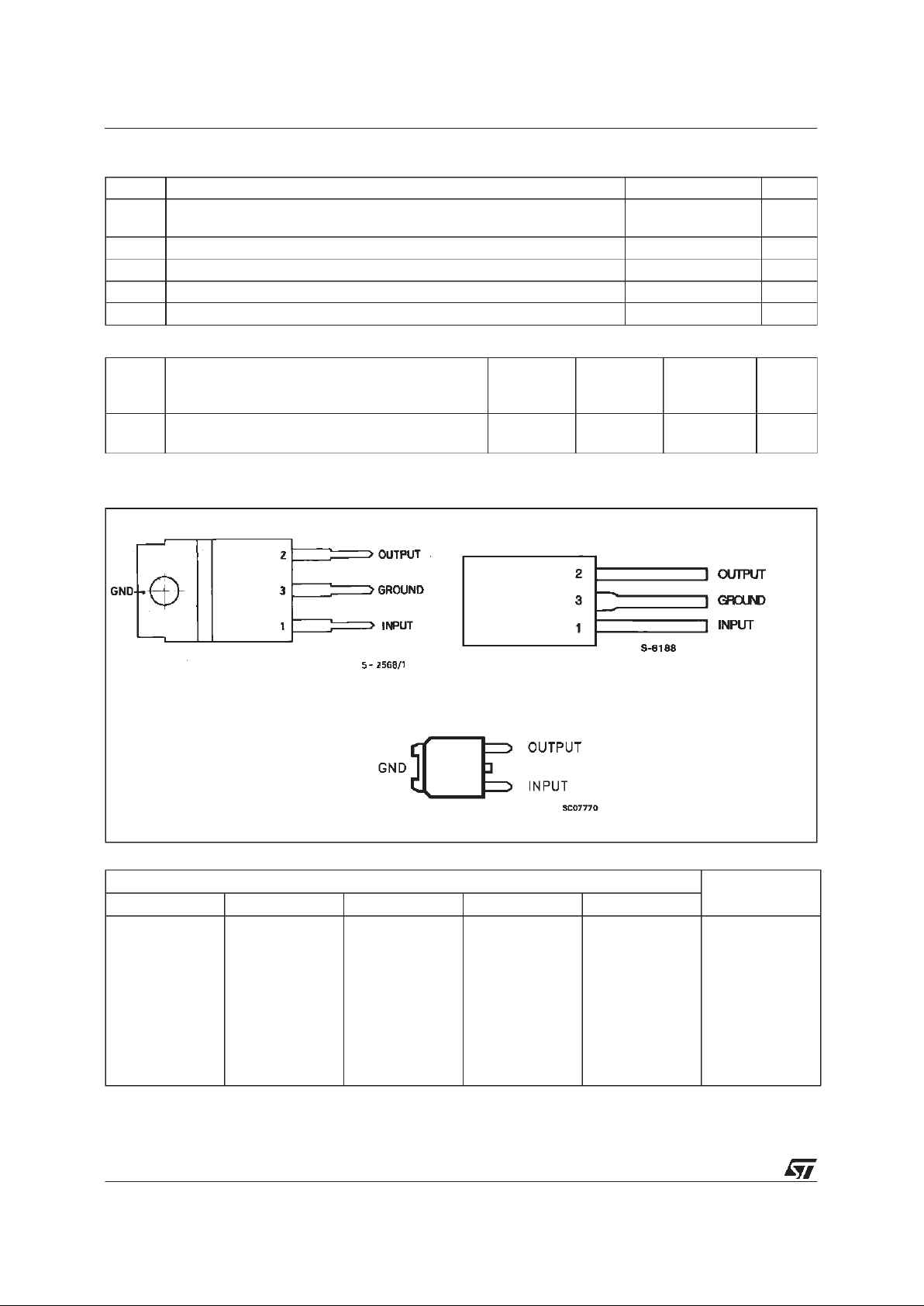
CONNECTION DIAGRAMAND ORDERING NUMBERS (top view)
Order Code Output Voltage
TO-220 ISOWATT220 SOT-82 SOT-194 DPAK
L78M05CV
L78M06CV
L78M08CV
L78M09CV
L78M10CV
L78M12CV
L78M15CV
L78M18CV
L78M20CV
L78M24CV
L78M0 5CP
L78M0 6CP
L78M0 8CP
L78M0 9CP
L78M1 0CP
L78M1 2CP
L78M1 5CP
L78M1 8CP
L78M2 0CP
L78M2 4CP
L78M05C X
L78M06C X
L78M08C X
L78M09C X
L78M10C X
L78M12C X
L78M15C X
L78M18C X
L78M20C X
L78M24C X
L78M05CS
L78M06CS
L78M08CS
L78M09CS
L78M10CS
L78M12CS
L78M15CS
L78M18CS
L78M20CS
L78M24CS
L78M05C DT
L78M06C DT
L78M08C DT
L78M09C DT
L78M10C DT
L78M12C DT
L78M15C DT
L78M18C DT
L78M20C DT
L78M24C DT
5V
6V
8V
9V
10V
12V
15V
18V
20V
24V
TO-220/ISOWATT220 SOT82/194
DPAK
L78M00
2/19
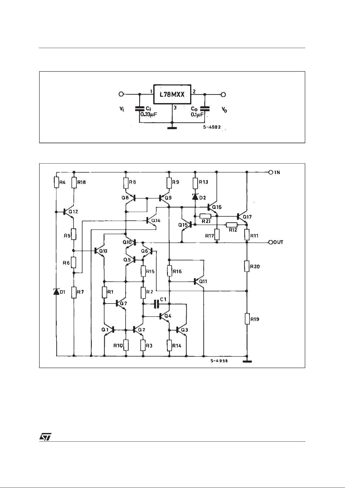
SCHEMATICDIAGRAM
APPLICATIONCIRCUIT
L78M00
3/19
TEST CIRCUITS
Figure1 : DC Parameters. Figure 2 : Load Regulation.
Figure3 : Ripple Rejection.
L78M00
4/19
ELECTRICALCHARACTERISTICS FOR L78M05C (refer to the test circuits, Tj=25oC,
V
i
=10V, Io=350 mA, Ci= 0.33 µF, Co= 0.1 µF unlessotherwisespecified)
Symbol Parameter Test Conditions Min. Typ. Max. Unit
V
o
OutputVoltage 4.8 5 5.2 V
V
o
OutputVoltage Io= 5mA to350mA
V
i
=7 to20 V
4.75 5 5.25 V
∆V
o
LineRegulation Io= 200mA Vi= 7 to25V
I
o
= 200mA Vi= 8 to25V
100
50
mV
mV
∆V
o
LoadRegulation Io= 5 to500 mA Tj=25oC
I
o
= 5 to200 mA Tj=25oC
100
50
mV
mV
I
d
Quiescent Current 6mA
∆I
d
Quiescent Current Change Io= 5 to350 mA 0.5 mA
∆I
d
Quiescent Current Change Io= 200mA Vi= 8 to25V 0.8 mA
∆
V
o
∆
T
OutputVoltage Drift Io= 5mA Tj= 0 to125oC-0.5mV/
o
C
e
N
OutputNoise Voltage B = 10Hz to100KHz 40
µV
SVR Supply Voltage Rejection I
o
= 300mA f = 120Hz
V
i
=8 to18 V
62 dB
V
d
Dropout Voltage 2 V
I
sc
ShortCircuitCurrent Vi=35V 300 m A
ELECTRICALCHARACTERISTICS FOR L78M06C (refer to the test circuits, Tj=25oC,
V
i
=11V, Io=350 mA, Ci= 0.33 µF, Co= 0.1 µF unlessotherwise specified)
Symbol Parameter Test Conditions Min. Typ. Max. Unit
V
o
OutputVoltage 5.75 6 6.25 V
V
o
OutputVoltage Io= 5 mA to350 mA
V
i
=8 to 21 V
5.766.3V
∆V
o
LineRegulation Io= 200 mA Vi= 8 to25 V
I
o
= 200 mA Vi= 9 to25 V
100
50
mV
mV
∆V
o
LoadRegulation Io= 5 to 500 mA Tj=25oC
I
o
= 5 to 200 mA Tj=25oC
120
60
mV
mV
I
d
Quiescent Current 6mA
∆I
d
Quiescent Current Change Io= 5 to 350 mA 0.5 mA
∆I
d
Quiescent Current Change Io= 200 mA Vi= 9 to 25 V 0.8 mA
∆
V
o
∆
T
OutputVoltage Drift Io= 5 mA Tj= 0 to 125oC-0.5mV/
o
C
e
N
OutputNoise Voltage B = 10Hz to 100KHz 45
µV
SVR Supply Voltage Rejection I
o
= 300 mA f = 120 Hz
V
i
=9 to 19 V
59 dB
V
d
Dropout Voltage 2 V
I
sc
ShortCircuit Current Vi=35V 270 m A
L78M00
5/19
ELECTRICALCHARACTERISTICS FOR L78M08C (refer to the test circuits, Tj=25oC,
V
i
=14V, Io=350 mA, Ci= 0.33 µF, Co= 0.1 µF unlessotherwise specified)
Symbol Parameter Test Conditions Min. Typ. Max. Unit
V
o
OutputVoltage 7.7 8 8.3 V
V
o
OutputVoltage Io= 5 mA to350 mA
V
i
=10.5 to 23 V
7.688.4V
∆V
o
LineRegulation Io= 200 mA Vi= 10.5 to 25 V
I
o
= 200 mA Vi=11to25V
100
50
mV
mV
∆V
o
LoadRegulation Io= 5 to 500 mA Tj=25oC
I
o
= 5 to 200 mA Tj=25oC
160
80
mV
mV
I
d
Quiescent Current 6mA
∆I
d
Quiescent Current Change Io= 5 to 350 mA 0.5 mA
∆I
d
Quiescent Current Change Io= 200 mA Vi= 10.5 to 25 V 0.8 mA
∆
V
o
∆
T
OutputVoltage Drift Io= 5 mA Tj= 0 to 125oC-0.5mV/
o
C
e
N
OutputNoise Voltage B = 10Hz to 100KHz 52
µV
SVR Supply Voltage Rejection I
o
= 300 mA f = 120 Hz
V
i
=11.5 to 21.5 V
56 dB
V
d
Dropout Voltage 2 V
I
sc
ShortCircuit Current Vi=35V 250 m A
ELECTRICALCHARACTERISTICS FOR L78M09C (refer to the test circuits, Tj=25oC,
V
i
=15V, Io=350 mA, Ci= 0.33 µF, Co= 0.1 µF unlessotherwise specified)
Symbol Parameter Test Conditions Min. Typ. Max. Unit
V
o
OutputVoltage 8.65 9 9.35 V
V
o
OutputVoltage Io= 5 mA to350 mA
V
i
=11.5 to 24 V
8.55 9 9.45 V
∆V
o
LineRegulation Io= 200 mA Vi= 11.5 to 25 V
I
o
= 200 mA Vi=12to25V
100
50
mV
mV
∆V
o
LoadRegulation Io= 5 to 500 mA Tj=25oC
I
o
= 5 to 200 mA Tj=25oC
180
90
mV
mV
I
d
Quiescent Current 6mA
∆I
d
Quiescent Current Change Io= 5 to 350 mA 0.5 mA
∆I
d
Quiescent Current Change Io= 200 mA Vi= 11.5 to 25 V 0.8 mA
∆
V
o
∆
T
OutputVoltage Drift Io= 5 mA Tj= 0 to 125oC-0.5mV/
o
C
e
N
OutputNoise Voltage B = 10Hz to 100KHz 58
µV
SVR Supply Voltage Rejection I
o
= 300 mA f = 120 Hz
V
i
=12.5 to 23 V
56 dB
V
d
Dropout Voltage 2 V
I
sc
ShortCircuit Current Vi=35V 250 m A
L78M00
6/19

ELECTRICALCHARACTERISTICS FOR L78M10C (refer to the test circuits, Tj=25oC,
V
i
=16V, Io=350 mA, Ci= 0.33 µF, Co= 0.1 µF unlessotherwise specified)
Symbol Parameter Test Conditions Min. Typ. Max. Unit
V
o
OutputVoltage 9.6 10 10.4 V
V
o
OutputVoltage Io= 5 mA to350 mA
V
i
=12.5 to 25 V
9.5 10 10.5 V
∆V
o
LineRegulation Io= 200 mA Vi= 12.5 to 30 V
I
o
= 200 mA Vi=13to30V
100
50
mV
mV
∆V
o
LoadRegulation Io= 5 to 500 mA Tj=25oC
I
o
= 5 to 200 mA Tj=25oC
200
100
mV
mV
I
d
Quiescent Current 6mA
∆I
d
Quiescent Current Change Io= 5 to 350 mA 0.5 mA
∆I
d
Quiescent Current Change Io= 200 mA Vi= 12.5 to 30 V 0.8 mA
∆
V
o
∆
T
OutputVoltage Drift Io= 5 mA Tj= 0 to 125oC-0.5mV/
o
C
e
N
OutputNoise Voltage B = 10Hz to 100KHz 64
µV
SVR Supply Voltage Rejection I
o
= 300 mA f = 120 Hz
V
i
=13.5 to 24 V
56 dB
V
d
Dropout Voltage 2 V
I
sc
ShortCircuit Current Vi=35V 245 m A
ELECTRICALCHARACTERISTICS FOR L78M12C (refer to the test circuits, Tj=25oC,
V
i
=19V, Io=350 mA, Ci= 0.33 µF, Co= 0.1 µF unlessotherwise specified)
Symbol Parameter Test Conditions Min. Typ. Max. Unit
V
o
OutputVoltage 11.5 12 12.5 V
V
o
OutputVoltage Io= 5 mA to350 mA
V
i
=14.5 to 27 V
11.4 12 12.6 V
∆V
o
LineRegulation Io= 200 mA Vi= 14.5 to 30 V
I
o
= 200 mA Vi=16to30V
100
50
mV
mV
∆V
o
LoadRegulation Io= 5 to 500 mA Tj=25oC
I
o
= 5 to 200 mA Tj=25oC
240
120
mV
mV
I
d
Quiescent Current 6mA
∆I
d
Quiescent Current Change Io= 5 to 350 mA 0.5 mA
∆I
d
Quiescent Current Change Io= 200 mA Vi= 14.5 to 30 V 0.8 mA
∆
V
o
∆
T
OutputVoltage Drift Io= 5 mA Tj= 0 to 125oC-1mV/
o
C
e
N
OutputNoise Voltage B = 10Hz to 100KHz 75
µV
SVR Supply Voltage Rejection I
o
= 300 mA f = 120 Hz
V
i
=15to25V
55 dB
V
d
Dropout Voltage 2 V
I
sc
ShortCircuit Current Vi=35V 240 m A
L78M00
7/19

ELECTRICALCHARACTERISTICS FOR L78M15C (refer to the test circuits, Tj=25oC,
V
i
=23V, Io=350 mA, Ci= 0.33 µF, Co= 0.1 µF unlessotherwise specified)
Symbol Parameter Test Conditions Min. Typ. Max. Unit
V
o
OutputVoltage 14.4 15 15.6 V
V
o
OutputVoltage Io= 5 mA to350 mA
V
i
=17.5 to 30 V
14.251515.75 V
∆V
o
LineRegulation Io= 200 mA Vi= 17.5 to 30 V
I
o
= 200 mA Vi=20to30V
100
50
mV
mV
∆V
o
LoadRegulation Io= 5 to 500 mA Tj=25oC
I
o
= 5 to 200 mA Tj=25oC
300
150
mV
mV
I
d
Quiescent Current 6mA
∆I
d
Quiescent Current Change Io= 5 to 350 mA 0.5 mA
∆I
d
Quiescent Current Change Io= 200 mA Vi= 17.5 to 30 V 0.8 mA
∆
V
o
∆
T
OutputVoltage Drift Io= 5 mA Tj= 0 to 125oC-1mV/
o
C
e
N
OutputNoise Voltage B = 10Hz to 100KHz 90
µV
SVR Supply Voltage Rejection I
o
= 300 mA f = 120 Hz
V
i
=18.5 to 28.5 V
54 dB
V
d
Dropout Voltage 2 V
I
sc
ShortCircuit Current Vi=35V 240 m A
ELECTRICALCHARACTERISTICS FOR L78M18C (refer to the test circuits, Tj=25oC,
V
i
=26V, Io=350 mA, Ci= 0.33 µF, Co= 0.1 µF unlessotherwise specified)
Symbol Parameter Test Conditions Min. Typ. Max. Unit
V
o
OutputVoltage 17.3 18 18.7 V
V
o
OutputVoltage Io= 5 mA to350 mA
V
i
=20.5 to 33 V
17.1 18 18.9 V
∆V
o
LineRegulation Io= 200 mA Vi=21to33V
I
o
= 200 mA Vi=24to33V
100
50
mV
mV
∆V
o
LoadRegulation Io= 5 to 500 mA Tj=25oC
I
o
= 5 to 200 mA Tj=25oC
360
180
mV
mV
I
d
Quiescent Current 6mA
∆I
d
Quiescent Current Change Io= 5 to 350 mA 0.5 mA
∆I
d
Quiescent Current Change Io= 200 mA Vi=21to33V 0.8 mA
∆
V
o
∆
T
OutputVoltage Drift Io= 5 mA Tj= 0 to 125oC-1.1mV/
o
C
e
N
OutputNoise Voltage B = 10Hz to 100KHz 100
µV
SVR Supply Voltage Rejection I
o
= 300 mA f = 120 Hz
V
i
=22to32V
53 dB
V
d
Dropout Voltage 2 V
I
sc
ShortCircuit Current Vi=35V 240 m A
L78M00
8/19

ELECTRICALCHARACTERISTICS FOR L78M20C (refer to the test circuits, Tj=25oC,
V
i
=29V, Io=350 mA, Ci= 0.33 µF, Co= 0.1 µF unlessotherwise specified)
Symbol Parameter Test Conditions Min. Typ. Max. Unit
V
o
OutputVoltage 19.2 20 20.8 V
V
o
OutputVoltage Io= 5 mA to350 mA
V
i
=23to35V
19 20 21 V
∆V
o
LineRegulation Io= 200 mA Vi=23to35V
I
o
= 200 mA Vi=24to35V
100
50
mV
mV
∆V
o
LoadRegulation Io= 5 to 500 mA Tj=25oC
I
o
= 5 to 200 mA Tj=25oC
400
200
mV
mV
I
d
Quiescent Current 6mA
∆I
d
Quiescent Current Change Io= 5 to 350 mA 0.5 mA
∆I
d
Quiescent Current Change Io= 200 mA Vi=23to35V 0.8 mA
∆
V
o
∆
T
OutputVoltage Drift Io= 5 mA Tj= 0 to 125oC-1.1mV/
o
C
e
N
OutputNoise Voltage B = 10Hz to 100KHz 110
µV
SVR Supply Voltage Rejection I
o
= 300 mA f = 120 Hz
V
i
=24to34V
53 dB
V
d
Dropout Voltage 2 V
I
sc
ShortCircuit Current Vi=35V 240 m A
ELECTRICALCHARACTERISTICS FOR L78M24C (refer to the test circuits, Tj=25oC,
V
i
=33V, Io=350 mA, Ci= 0.33 µF, Co= 0.1 µF unlessotherwise specified)
Symbol Parameter Test Conditions Min. Typ. Max. Unit
V
o
OutputVoltage 23 24 25 V
V
o
OutputVoltage Io= 5 mA to350 mA
V
i
=27to38V
22.8 24 25.2 V
∆V
o
LineRegulation Io= 200 mA Vi=27to38V
I
o
= 200 mA Vi=28to38V
100
50
mV
mV
∆V
o
LoadRegulation Io= 5 to 500 mA Tj=25oC
I
o
= 5 to 200 mA Tj=25oC
480
240
mV
mV
I
d
Quiescent Current 6mA
∆I
d
Quiescent Current Change Io= 5 to 350 mA 0.5 mA
∆I
d
Quiescent Current Change Io= 200 mA Vi=27to38V 0.8 mA
∆
V
o
∆
T
OutputVoltage Drift Io= 5 mA Tj= 0 to 125oC-1.2mV/
o
C
e
N
OutputNoise Voltage B = 10Hz to 100KHz 170
µV
SVR Supply Voltage Rejection I
o
= 300 mA f = 120 Hz
V
i
=28to38V
50 dB
V
d
Dropout Voltage 2 V
I
sc
ShortCircuit Current Vi=35V 240 m A
L78M00
9/19

Figure4 : Dropout Voltage vs. Junction
Temperature.
Figure 5 : Dropout Characteristics.
Figure6 : Peak Output Currentvs. Input-Output
DifferentialVoltage.
Figure 7 : Output Voltage vs. Junction
Temperature.
Figure8 : SupplyVoltage Rejection vs.
Frequency.
Figure 9 : Quiescent Current vs. Junction
Temperature.
L78M00
10/19

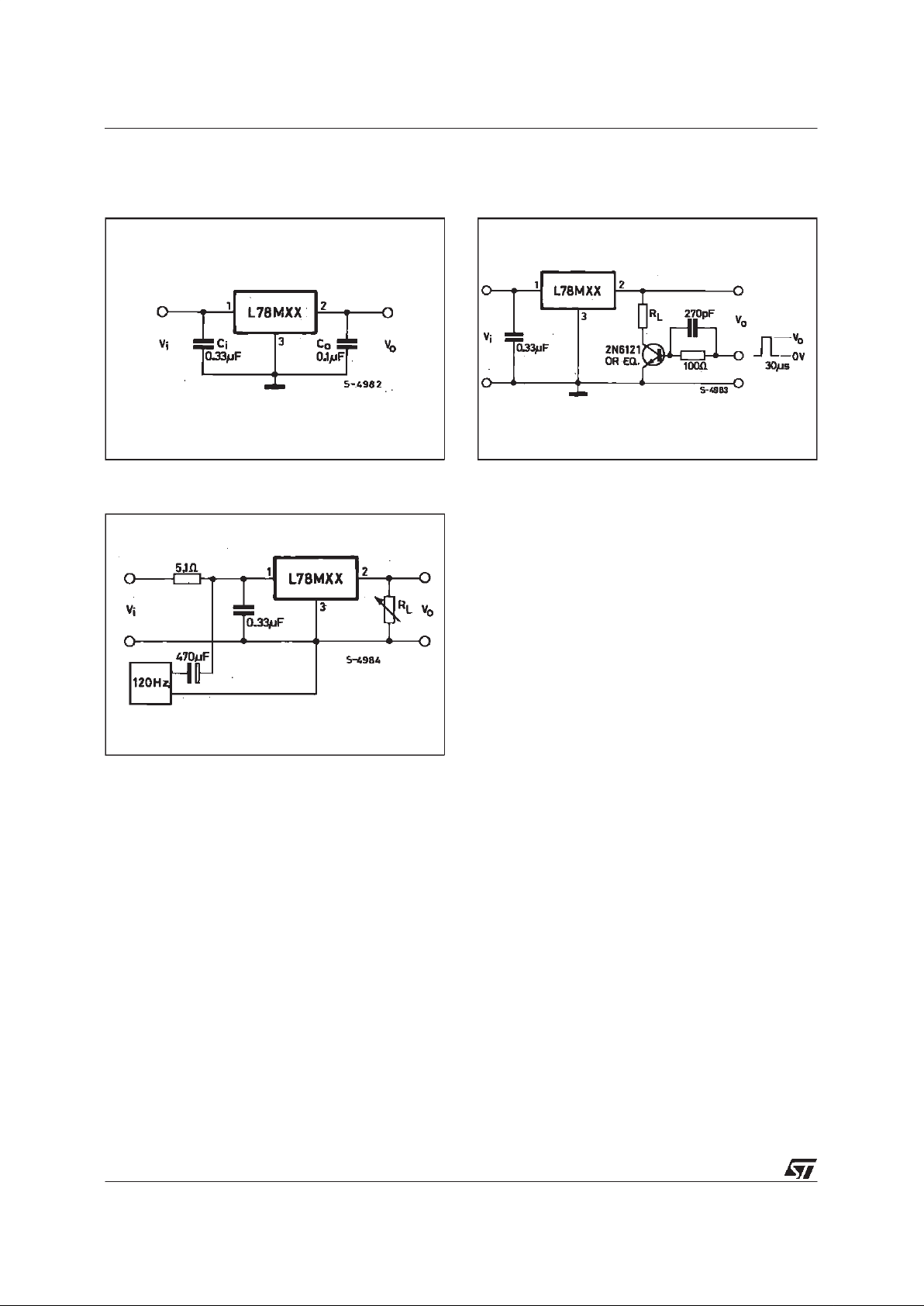
Figure12 : QuiescentCurrentvs. InputVoltage. Figure 13 : Fixed Output Regulator.
Figure10 : Load TransientResponse. Figure 11 : Line Transient Response.
NOTE:
1. To specify an output voltage, substitute voltage value for ”XX”.
2. Although no output capacitor is need for stability, it does
improve transient response.
3. Required if cregulator is locate an appreciable distance from
power supply filter.
I
O
=
V
XX
R
1
+
I
d
IR1≥ 5I
d
VO=
V
XX
(1 +
R
2
R
1
)
+
IdR
2
L78M00
11/19

Figure16 : AdjustableOutput Regulator
(7 to 30V).
Figure 17 : 0.5 to 10V Regulator.
Figure18 : High CurrentVoltage Regulator. Figure 19 : High Output Current with Short
Circuit
Figure20 : TrackingVoltageRegulator. Figure21 : HighInput VoltageCircuit.
VO =
V
XX
R
4
R
1
R1=
V
BEQ
1
I
REQ
−
I
Q
1
β
Q
1
IO=
I
REG
+
Q
1
(
I
REG
−
V
BEQ
1
R
1
)
V
IN=Vi
-(VZ+VBE)
R
SC
=
V
BEQ
2
I
SC
L78M00
12/19

Figure22 : Reducing PowerDissipation with
DroppingResistor.
Figure 23 : PowerAM Modulator (unity voltage
gain, Io ≤ 0.5).
Figure24 : AdjustableOutput Voltage with Tem-
peratureCompensation.
R=
V
i(min
)
−
V
XX
−
V
DROP(max
)
I
O(max
)
+
I
d(max
)
NOTE: The circuit performs well upto 100KHz
NOTE: Q
2
is connected as a diode in order to compensate the
variation of the Q
1VBE
with the temperature. C allows a slow rise-
time of the V
o
VO=
V
XX
(1 +
R
2
R
1
)
+
V
BE
L78M00
13/19

DIM.
mm inch
MIN. TYP. MAX. MIN. TYP. MAX.
A 7.4 7.8 0.291 0.307
B 10.5 11.3 0.413 0.445
b 0.7 0.9 0.028 0.035
b1 0.49 0.75 0.019 0.030
C 2.4 2.7 0.04 0.106
c1 1.2 0.047
D 15.7 0.618
e 2.2 0.087
e3 4.4 0.173
F 3.8 0.150
H 2.54 0.100
F
A
H
BD
e3
e
b1
c1
C
b
SOT-82 MECHANICALDATA
P032A
L78M00
14/19

DIM.
mm inch
MIN. TYP. MAX. MIN. TYP. MAX.
A 7.4 7.8 0.291 0.307
B 10.5 11.3 0.413 0.445
b 0.7 0.9 0.028 0.035
b1 0.49 0.75 0.019 0.030
C 2.4 2.7 0.094 0.106
c1 1.2 0.047
c2 1.3 0.051
D 6 0.236
e 2.2 0.087
e3 4.4 0.173
F 3.8 0.150
H 2.54 0.100
P 45 (typ.)
S 4 0.157
S1 2 0.079
T 0.1 0.004
F
A
H
B
D
e3
e
b1
c2
C
b
P
T
C1
SS1
P032B
SOT-194 MECHANICAL DATA
L78M00
15/19

DIM.
mm inch
MIN. TYP. MAX. MIN. TYP. MAX.
A 2.2 2.4 0.086 0.094
A1 0.9 1.1 0.035 0.043
A2 0.03 0.23 0.001 0.009
B 0.64 0.9 0.025 0.035
B2 5.2 5.4 0.204 0.212
C 0.45 0.6 0.017 0.023
C2 0.48 0.6 0.019 0.023
D 6 6.2 0.236 0.244
E 6.4 6.6 0.252 0.260
G 4.4 4.6 0.173 0.181
H 9.35 10.1 0.368 0.397
L2 0.8 0.031
L4 0.6 1 0.023 0.039
==
D
L2
L4
13
==
B
E
==
B2
G
2
A
C2
C
H
A1
DETAIL”A”
A2
DETAIL”A”
TO-252 (DPAK) MECHANICAL DATA
0068772-B
L78M00
16/19

DIM.
mm inch
MIN. TYP. MAX. MIN. TYP. MAX.
A 4.40 4.60 0.173 0.181
C 1.23 1.32 0.048 0.051
D 2.40 2.72 0.094 0.107
D1 1.27 0.050
E 0.49 0.70 0.019 0.027
F 0.61 0.88 0.024 0.034
F1 1.14 1.70 0.044 0.067
F2 1.14 1.70 0.044 0.067
G 4.95 5.15 0.194 0.203
G1 2.4 2.7 0.094 0.106
H2 10.0 10.40 0.393 0.409
L2 16.4 0.645
L4 13.0 14.0 0.511 0.551
L5 2.65 2.95 0.104 0.116
L6 15.25 15.75 0.600 0.620
L7 6.2 6.6 0.244 0.260
L9 3.5 3.93 0.137 0.154
DIA. 3.75 3.85 0.147 0.151
L6
A
C
D
E
D1
F
G
L7
L2
Dia.
F1
L5
L4
H2
L9
F2
G1
TO-220 MECHANICALDATA
P011C
L78M00
17/19

DIM.
mm inch
MIN. TYP. MAX. MIN. TYP. MAX.
A 4.4 4.6 0.173 0.181
B 2.5 2.7 0.098 0.106
D 2.5 2.75 0.098 0.108
E 0.4 0.7 0.015 0.027
F 0.75 1 0.030 0.039
F1 1.15 1.7 0.045 0.067
F2 1.15 1.7 0.045 0.067
G 4.95 5.2 0.195 0.204
G1 2.4 2.7 0.094 0.106
H 10 10.4 0.393 0.409
L2 16 0.630
L3 28.6 30.6 1.126 1.204
L4 9.8 10.6 0.385 0.417
L6 15.9 16.4 0.626 0.645
L7 9 9.3 0.354 0.366
Ø 3 3.2 0.118 0.126
L2
A
B
D
E
H
G
L6
¯
F
L3
G1
123
F2
F1
L7
L4
ISOWATT220MECHANICAL DATA
P011G
L78M00
18/19

Information furnished is believed to be accurate and reliable. However, STMicroelectronics assumes no responsibility for the consequences
of use of such information nor for any infringement of patents or other rights of third parties which may result from its use. No license is
granted by implication or otherwise under any patent or patent rights of STMicroelectronics. Specification mentioned in this publication are
subject to change without notice. This publication supersedes and replaces all information previously supplied. STMicroelectronics products
are not authorized for use as critical components in life support devices or systems without express written approval ofSTMicroelectronics.
The ST logo is a trademark of STMicroelectronics
1998 STMicroelectronics – Printed in Italy – All Rights Reserved
STMicroelectronics GROUP OF COMPANIES
Australia - Brazil - Canada - China - France - Germany - Italy - Japan - Korea - Malaysia - Malta - Mexico - Morocco- The Netherlands -
Singapore - Spain - Sweden - Switzerland - Taiwan - Thailand - United Kingdom - U.S.A.
.
L78M00
19/19
 Loading...