

SGS Thomson Microelectronics L78L15ACUTR, L78L24ACUTR, L78L15ABUTR, L78L12ACUTR, L78L12ABUTR Datasheet
...
1/24July 2003
■ OUTPUT CURRENT UP TO 100 mA
■ OUTPUT VOLTAGES OF 3.3; 5; 6; 8; 9; 10;
12; 15; 18; 20; 24V
■ THERMAL OVERLOAD PROTECTION
■ SHORT CIRCUIT PROTECTION
■ NO EXTERNAL COMPONENTS A RE
REQUIRED
■ AVAILABLE IN EITHER ±5% (AC) OR ±10%
(C) SELECTION
DESCRIPTION
The L78L00 series of three-terminal positive
regulators employ internal current limiting and
thermal shutdown, making them essen tially
indestructible. If adequate heat-sink is provided,
they can deliverup to 100 mA output current. T hey
are i nte nded as fixed volt age regulators in a wide
range of applications including local or on-card
regulation for elimination of noise and distribution
problems associated with single-poi nt regulation.
In addition, they c an be used with power pass
elements to make high-current voltage regulators.
The L78L00 series used as Zener diode/resistor
combination replacement, offers an effective
output impedanc e improvement of typically t wo
orders of magnitude, along with lower quiescent
current and lower noise.
L78L00
SERIES
POSITIVE VOLTAGE REGULATORS
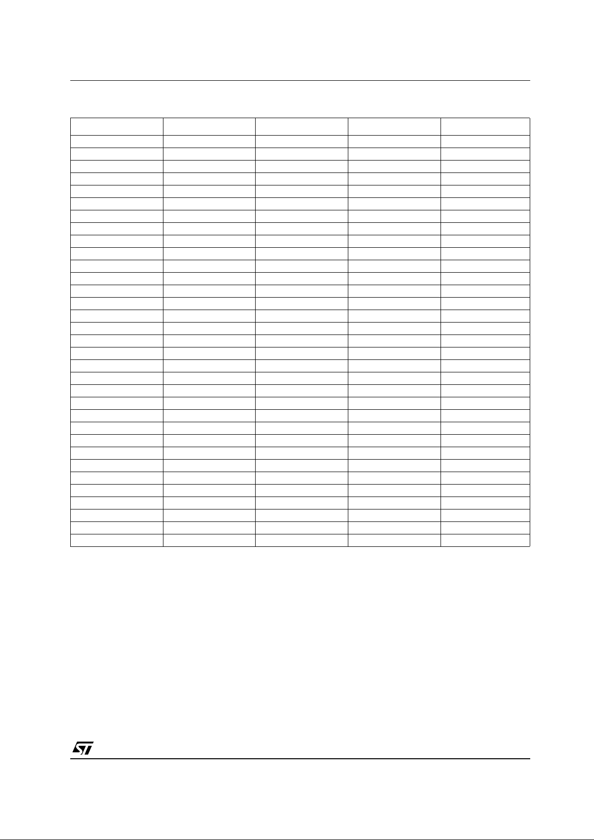
SCHEMATIC DIAGRAM
TO-92
SOT-89SO-8
L78L00 SERIES
2/24
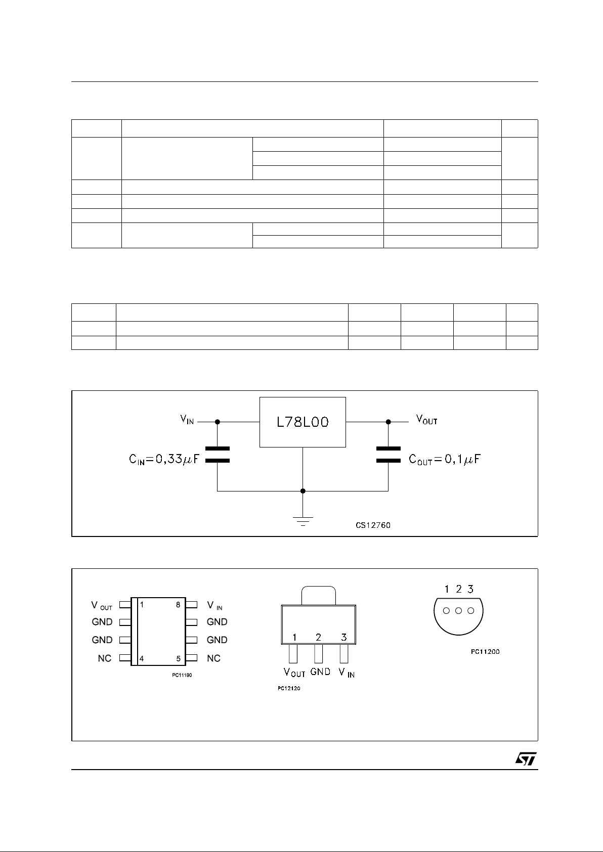
ABSOLUTE MAXIMUM RATINGS
(*) Our SO-8 package used for Voltage Regulators is modified internally to have pins 2, 3, 6 and 7 electrically communed to the die attach
flag. This particular frame decreases the total thermal resistance of the package and increases its ability to dissipate power when a n appropriate area of copper on the printed circuit board is available for heat-sinking. The external dimensions are the same as forthestandard SO-8.
THERMAL DATA
(*) Considering 6 cm2of copper Board heat-sink
TEST CIRCUITS
CONNECTION DIAGRAM (top view)
Symbol Parameter² Value Unit
V
I
DC Input Voltage VO= 3.3 to 9 V
30
V
V
O
=12to15V
35
V
O
=18to24V
40
I
O
Output Current
100 mA
P
tot
Power Dissipation
Internally Limited (*)
T
stg
Storage Temperature Range
-40 to 150 °C
T
op
OperatingJunctionTemperature
Range
for L78L00C, L78L00AC 0 to 125
°C
for L78L00AB -40 to 125
Symbol Parameter SO-8 TO-92 SOT-89 Unit
R
thj-case
Thermal Resistance Junction-case Max
20 15 °C/W
R
thj-amb
Thermal Resistance Junction-ambient Max
55 (*) 200 °C/W
SOT-89SO-8
BOTTOM VIEW
PIN 1 = V
OUT
PIN 2 = GND
PIN 3 = V
IN
TO-92
L78L00 SE RIE S
3/24
ORDERING CODES
(*) Available in Tape & Reel with the suffix "13TR".
(**) Available in Ammopak with the suffix "-AP" or in Tape & Reel with the suffix "TR".
TYPE SO-8 (TUBE)* TO-92 (TUBE)** SOT-89 (T&R) OUTPUT VOLTAGE
L78L33C L78L33CD L78L33CZ 3.3 V
L78L33AC L78L33ACD L78L33ACZ L78L33ACUTR 3.3 V
L78L33AB L78L33ABD L78L33ABZ L78L33ABUTR 3.3 V
L78L05C L78L05CD L78L05CZ 5 V
L78L05AC L78L05ACD L78L05ACZ L78L05ACUTR 5 V
L78L05AB L78L05ABD L78L05ABZ L78L05ABUTR 5 V
L78L06C L78L06CD L78L06CZ 6 V
L78L06AC L78L06ACD L78L06ACZ L78L06ACUTR 6 V
L78L06AB L78L06ABD L78L06ABZ L78L06ABUTR 6 V
L78L08C L78L08CD L78L08CZ 8 V
L78L08AC L78L08ACD L78L08ACZ L78L08ACUTR 8 V
L78L08AB L78L08ABD L78L08ABZ L78L08ABUTR 8 V
L78L09C L78L09CD L78L09CZ 9 V
L78L09AC L78L09ACD L78L09ACZ L78L09ACUTR 9 V
L78L09AB L78L09ABD L78L09ABZ L78L09ABUTR 9 V
L78L10C L78L10CD L78L10CZ 10 V
L78L10AC L78L10ACD L78L10ACZ L78L10ACUTR 10 V
L78L10AB L78L10ABD L78L10ABZ L78L10ABUTR 10 V
L78L12C L78L12CD L78L12CZ 12 V
L78L12AC L78L12ACD L78L12ACZ L78L12ACUTR 12 V
L78L12AB L78L12ABD L78L12ABZ L78L12ABUTR 12 V
L78L15C L78L15CD L78L15CZ 15 V
L78L15AC L78L15ACD L78L15ACZ L78L15ACUTR 15 V
L78L15AB L78L15ABD L78L15ABZ L78L15ABUTR 15 V
L78L18C L78L18CD L78L18CZ 18 V
L78L18AC L78L18ACD L78L18ACZ L78L18ACUTR 18 V
L78L18AB L78L18ABD L78L18ABZ L78L18ABUTR 18 V
L78L20C L78L20CD L78L20CZ 20 V
L78L20AC L78L20ACD L78L20ACZ L78L20ACUTR 20 V
L78L20AB L78L20ABD L78L20ABZ L78L20ABUTR 20 V
L78L24C L78L24CD L78L24CZ 24 V
L78L24AC L78L24ACD L78L24ACZ L78L24ACUTR 24 V
L78L24AB L78L24ABD L78L24ABZ L78L24ABUTR 24 V

L78L00 SERIES
4/24
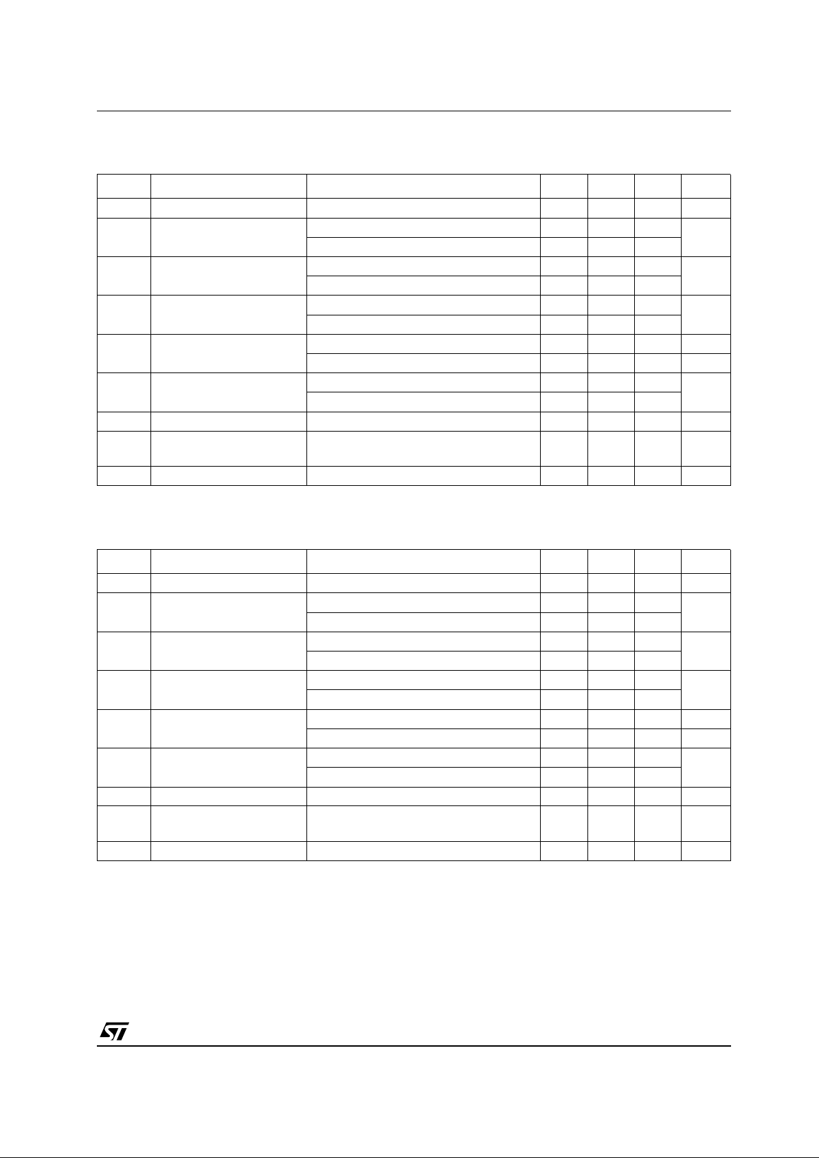
ELECTRICAL CHARACTERISTICS OF L78L33C (refer to the test circuits, TJ= 0 to 125°C, VI=8.3V,
I
O
=40mA,CI=0.33µF,CO= 0.1 µ F unless otherwise specified)
ELECTRICAL CHARACTERISTICS OF L78L05C (refer to the test circuits, T
J
= 0 to 125°C, VI=10V,
I
O
=40mA,CI=0.33µF,CO= 0.1 µ F unless otherwise specified).
Symbol Parameter Test Conditions Min. Typ. Max. Unit
V
O
Output Voltage TJ= 25°C 3.036 3.3 3.564 V
V
O
Output Voltage IO= 1 to 40 mA VI= 5.3 to 20 V 2.97 3.63 V
I
O
= 1 to 70 mA VI= 8.3 V 2.97 3.63
∆V
O
Line Regulation VI= 5.3 to 20 V TJ= 25°C 150 mV
V
I
= 6.3 to 20 V TJ= 25°C 100
∆V
O
Load Regulation IO= 1 to 100 mA TJ= 25°C 60 mV
I
O
=1to40mA TJ= 25°C 30
I
d
Quiescent Current TJ= 25°C 6 mA
T
J
= 125°C 5.5 mA
∆I
d
Quiescent Current Change IO=1to40mA 0.2 mA
V
I
= 6.3 to 20 V 1.5
eN Output Noise Voltage B =10Hz to 100KHz T
J
= 25°C 40 µV
SVR Supply Voltage Rejection V
I
= 6.3 to 16.3 V f = 120Hz
I
O
=40mA TJ= 25°C
41 49 dB
V
d
Dropout Voltage 1.7 V
Symbol Parameter Test Conditions Min. Typ. Max. Unit
V
O
Output Voltage TJ= 25°C 4.6 5 5.4 V
V
O
Output Voltage IO= 1 to 40 mA VI=7 to 20 V 4.5 5.5 V
I
O
= 1 to 70 mA VI= 10 V 4.5 5.5
∆V
O
Line Regulation VI= 8.5 to 20 V TJ= 25°C 200 mV
V
I
=9to20V TJ= 25°C 150
∆V
O
Load Regulation IO= 1 to 100 mA TJ= 25°C 60 mV
I
O
=1to40mA TJ= 25°C 30
I
d
Quiescent Current TJ= 25°C 6 mA
T
J
= 125°C 5.5 mA
∆I
d
Quiescent Current Change IO=1to40mA 0.2 mA
V
I
= 8 to 20 V 1.5
eN Output Noise Voltage B =10Hz to 100KHz T
J
= 25°C 40 µV
SVR Supply Voltage Rejection V
I
= 9 to 20 V f = 120Hz
I
O
=40mA TJ= 25°C
40 49 dB
V
d
Dropout Voltage 1.7 V
L78L00 SE RIE S
5/24
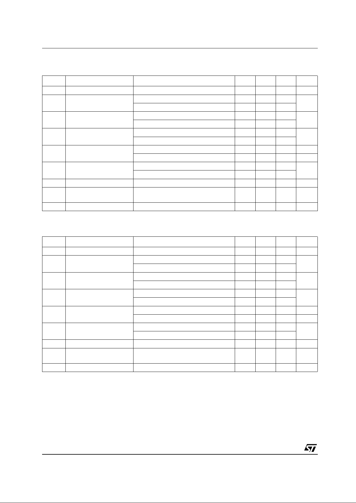
ELECTRICAL CHARACTERISTICS OF L78L06C (refer to the test circuits, TJ= 0 to 125°C, VI=12V,
I
O
=40mA,CI=0.33µF,CO= 0.1 µ F unless otherwise specified).
ELECTRICAL CHARACTERISTICS OF L78L08C (refer to the test circuits, T
J
= 0 to 125°C, VI=14V,
I
O
=40mA,CI=0.33µF,CO= 0.1 µ F unless otherwise specified).
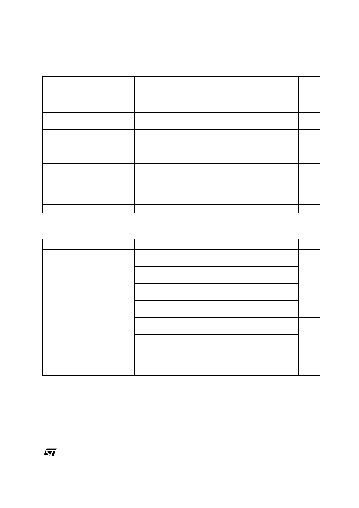
Symbol Parameter Test Conditions Min. Typ. Max. Unit
V
O
Output Voltage TJ= 25°C 5.52 6 6.48 V
V
O
Output Voltage IO= 1 to 40 mA VI=8.5 to 20 V 5.4 6.6 V
I
O
= 1 to 70 mA VI= 12 V 5.4 6.6
∆V
O
Line Regulation VI= 8.5 to 20 V TJ= 25°C 200 mV
V
I
=9to20V TJ= 25°C 150
∆V
O
Load Regulation IO= 1 to 100 mA TJ= 25°C 60 mV
I
O
=1to40mA TJ= 25°C 30
I
d
Quiescent Current TJ= 25°C 6 mA
T
J
= 125°C 5.5 mA
∆I
d
Quiescent Current Change IO=1to40mA 0.2 mA
V
I
= 8 to 20 V 1.5
eN Output Noise Voltage B =10Hz to 100KHz T
J
= 25°C 50 µV
SVR Supply Voltage Rejection V
I
= 9 to 20 V f = 120Hz
I
O
=40mA TJ= 25°C
38 46 dB
V
d
Dropout Voltage 1.7 V
Symbol Parameter Test Conditions Min. Typ. Max. Unit
V
O
Output Voltage TJ= 25°C 7.36 8 8.64 V
V
O
Output Voltage IO= 1 to 40 mA VI=10.5 to 23 V 7.2 8.8 V
I
O
= 1 to 70 mA VI= 14 V 7.2 8.8
∆V
O
Line Regulation VI= 10.5 to 23 V TJ= 25°C 200 mV
V
I
=11to23V TJ= 25°C 150
∆V
O
Load Regulation IO= 1 to 100 mA TJ= 25°C 80 mV
I
O
=1to40mA TJ= 25°C 40
I
d
Quiescent Current TJ= 25°C 6 mA
T
J
= 125°C 5.5 mA
∆I
d
Quiescent Current Change IO=1to40mA 0.2 mA
V
I
=11to23V 1.5
eN Output Noise Voltage B =10Hz to 100KHz T
J
= 25°C 60 µV
SVR Supply Voltage Rejection V
I
= 12 to 23 V f = 120Hz
I
O
=40mA TJ= 25°C
36 45 dB
V
d
Dropout Voltage 1.7 V
L78L00 SERIES
6/24
ELECTRICAL CHARACTERISTICS OF L78L09C (refer to the test circuits, TJ= 0 to 125°C, VI=15V,
I
O
=40mA,CI=0.33µF,CO= 0.1 µ F unless otherwise specified).
ELECTRICAL CHARACTERISTICS OF L78L10C (refer to the test circuits, T
J
= 0 to 125°C, VI=16V,
I
O
=40mA,CI=0.33µF,CO= 0.1 µ F unless otherwise specified).
Symbol Parameter Test Conditions Min. Typ. Max. Unit
V
O
Output Voltage TJ= 25°C 8.28 9 9.72 V
V
O
Output Voltage IO= 1 to 40 mA VI=11.5 to 23 V 8.1 9.9 V
I
O
= 1 to 70 mA VI= 15 V 8.1 9.9
∆V
O
Line Regulation VI= 11.5 to 23 V TJ= 25°C 250 mV
V
I
=12to23V TJ= 25°C 200
∆V
O
Load Regulation IO= 1 to 100 mA TJ= 25°C 80 mV
I
O
=1to40mA TJ= 25°C 40
I
d
Quiescent Current TJ= 25°C 6 mA
T
J
= 125°C 5.5 mA
∆I
d
Quiescent Current Change IO=1to40mA 0.2 mA
V
I
=12to23V 1.5
eN Output Noise Voltage B =10Hz to 100KHz T
J
= 25°C 70 µV
SVR Supply Voltage Rejection V
I
= 12 to 23 V f = 120Hz
I
O
=40mA TJ= 25°C
36 44 dB
V
d
Dropout Voltage 1.7 V
Symbol Parameter Test Conditions Min. Typ. Max. Unit
V
O
Output Voltage TJ= 25°C 9.2 10 10.8 V
V
O
Output Voltage IO= 1 to 40 mA VI=12.5 to 23 V 9 11 V
I
O
= 1 to 70 mA VI=16V 9 11
∆V
O
Line Regulation VI= 12.5 to 23 V TJ= 25°C 230 mV
V
I
=13to23V TJ= 25°C 170
∆V
O
Load Regulation IO= 1 to 100 mA TJ= 25°C 80 mV
I
O
=1to40mA TJ= 25°C 40
I
d
Quiescent Current TJ= 25°C 6 mA
T
J
= 125°C 5.5 mA
∆I
d
Quiescent Current Change IO=1to40mA 0.1 mA
V
I
=13to23V 1.5
eN Output Noise Voltage B =10Hz to 100KHz T
J
= 25°C 60 µV
SVR Supply Voltage Rejection V
I
= 14 to 23 V f = 120Hz
I
O
=40mA TJ= 25°C
37 45 dB
V
d
Dropout Voltage 1.7 V
L78L00 SE RIE S
7/24
ELECTRICAL CHARACTERISTICS OF L78L12C (refer to the test circuits, TJ= 0 to 125°C, VI=19V,
I
O
=40mA,CI=0.33µF,CO= 0.1 µ F unless otherwise specified).
ELECTRICAL CHARACTERISTICS OF L78L15C (refer to the test circuits, T
J
= 0 to 125°C, VI=23V,
I
O
=40mA,CI=0.33µF,CO= 0.1 µ F unless otherwise specified).
Symbol Parameter Test Conditions Min. Typ. Max. Unit
V
O
Output Voltage TJ= 25°C 11.1 12 12.9 V
V
O
Output Voltage IO= 1 to 40 mA VI=14.5 to 27 V 10.8 13.2 V
I
O
= 1 to 70 mA VI= 19 V 10.8 13.2
∆V
O
Line Regulation VI= 14.5 to 27 V TJ= 25°C 250 mV
V
I
=16to27V TJ= 25°C 200
∆V
O
Load Regulation IO= 1 to 100 mA TJ= 25°C 100 mV
I
O
=1to40mA TJ= 25°C 50
I
d
Quiescent Current TJ= 25°C 6.5 mA
T
J
= 125°C 6 mA
∆I
d
Quiescent Current Change IO=1to40mA 0.2 mA
V
I
=16to27V 1.5
eN Output Noise Voltage B =10Hz to 100KHz T
J
= 25°C 80 µV
SVR Supply Voltage Rejection V
I
= 15 to 25 V f = 120Hz
I
O
=40mA TJ= 25°C
36 42 dB
V
d
Dropout Voltage 1.7 V
Symbol Parameter Test Conditions Min. Typ. Max. Unit
V
O
Output Voltage TJ= 25°C 13.8 15 16.2 V
V
O
Output Voltage IO= 1 to 40 mA VI=17.5 to 30 V 13.5 16.5 V
I
O
= 1 to 70 mA VI= 23 V 13.5 16.5
∆V
O
Line Regulation VI= 17.5 to 30 V TJ= 25°C 300 mV
V
I
=20to30V TJ= 25°C 250
∆V
O
Load Regulation IO= 1 to 100 mA TJ= 25°C 150 mV
I
O
=1to40mA TJ= 25°C 75
I
d
Quiescent Current TJ= 25°C 6.5 mA
T
J
= 125°C 6 mA
∆I
d
Quiescent Current Change IO=1to40mA 0.2 mA
V
I
=20to30V 1.5
eN Output Noise Voltage B =10Hz to 100KHz T
J
= 25°C 90 µV
SVR Supply Voltage Rejection V
I
= 18.5 to 28.5 V f = 120Hz
I
O
=40mA TJ= 25°C
33 39 dB
V
d
Dropout Voltage 1.7 V

L78L00 SERIES
8/24
ELECTRICAL CHARACTERISTICS OF L78L18C (refer to the test circuits, TJ= 0 to 125°C, VI=27V,
I
O
=40mA,CI=0.33µF,CO= 0.1 µ F unless otherwise specified).
ELECTRICAL CHARACTERISTICS OF L78L20C (refer to the test circuits, T
J
= 0 to 125°C, VI=29V,
I
O
=40mA,CI=0.33µF,CO= 0.1 µ F unless otherwise specified)
Symbol Parameter Test Conditions Min. Typ. Max. Unit
V
O
Output Voltage TJ= 25°C 16.6 18 19.4 V
V
O
Output Voltage IO= 1 to 40 mA VI=22to33V 16.2 19.8 V
I
O
= 1 to 70 mA VI= 27 V 16.2 19.8
∆V
O
Line Regulation VI=22to33V TJ= 25°C 320 mV
V
I
=22to33V TJ= 25°C 270
∆V
O
Load Regulation IO= 1 to 100 mA TJ= 25°C 170 mV
I
O
=1to40mA TJ= 25°C 85
I
d
Quiescent Current TJ= 25°C 6.5 mA
T
J
= 125°C 6 mA
∆I
d
Quiescent Current Change IO=1to40mA 0.2 mA
V
I
=23to33V 1.5
eN Output Noise Voltage B =10Hz to 100KHz T
J
= 25°C 120 µV
SVR Supply Voltage Rejection V
I
= 23 to 33 V f = 120Hz
I
O
=40mA TJ= 25°C
32 38 dB
V
d
Dropout Voltage 1.7 V
Symbol Parameter Test Conditions Min. Typ. Max. Unit
V
O
Output Voltage TJ= 25°C 18.4 20 21.6 V
V
O
Output Voltage IO= 1 to 40 mA VI=24to33V 18 22 V
I
O
= 1 to 70 mA VI=29V 18 22
∆V
O
Line Regulation VI= 22.5 to 34 V TJ= 25°C 330 mV
V
I
=24to34V TJ= 25°C 280
∆V
O
Load Regulation IO= 1 to 100 mA TJ= 25°C 180 mV
I
O
=1to40mA TJ= 25°C 90
I
d
Quiescent Current TJ= 25°C 6.5 mA
T
J
= 125°C 6 mA
∆I
d
Quiescent Current Change IO=1to40mA 0.2 mA
V
I
=25to33V 1.5
eN Output Noise Voltage B =10Hz to 100KHz T
J
= 25°C 120 µV
SVR Supply Voltage Rejection V
I
= 25 to 35 V f = 120Hz
I
O
=40mA TJ= 25°C
31 38 dB
V
d
Dropout Voltage 1.7 V
 Loading...