

Datasheet L78L24ABZ, L78L24ABD, L78L18CZ, L78L18CD, L78L18ACZ Datasheet (SGS Thomson Microelectronics)
...
L78L00
SERIES
POSITIVE VOLTAGE REGULATORS
February 1999
■ OUTPUT CURRENT UPTO100 mA
■
OUTPUT VOLTAGESOF 3.3;5; 6; 8; 9; 12;
15;18; 24V
■
THERMAL OVERLOADPROTECTION
■ SHORTCIRCUIT PROTECTION
■ NOEXTERNALCOMPONENTS ARE
REQUIRED
■ AVAILABLEIN EITHER± 5% (AC)OR ± 10%
(C)SELECTION
DESCRIPTION
The L78L00 series of three-terminal positive
regulators employ internal current limiting and
thermal shutdown, making them essentially
indestructible. If adequate heatsink is provided,
they can deliver up to 100 mA output current.
They are intended as fixed voltage regulatorsin a
wide range of applications including local or
on-card regulation for elimination of noise and
distribution problems associated with single-point
regulation. In addition, they can be used with
power pass elements to make high-current
voltageregulators.
The L78L00 series used as Zener diode/resistor
combination replacement, offers an effective
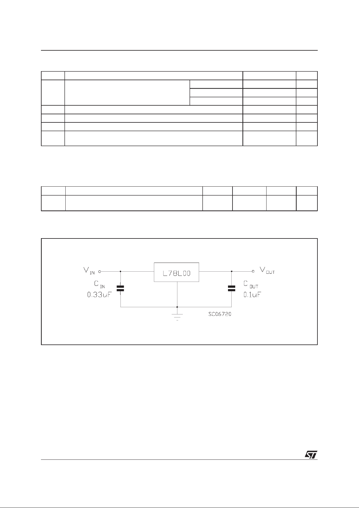
BLOCKDIAGRAM
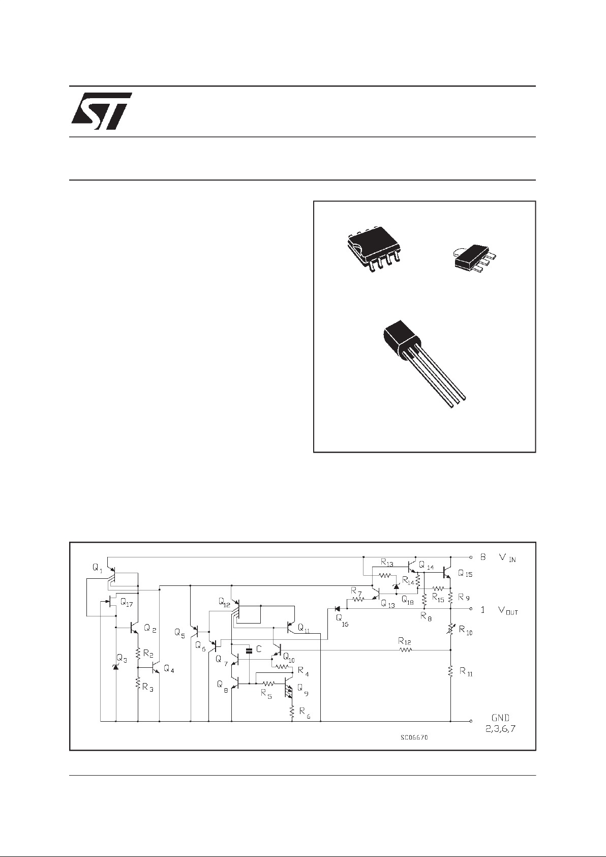
SO-8
TO-92
output impedance improvement of typically two
orders of magnetude, along with lower quiescent
currentand lower noise.
SOT-89
1/19
ABSOLUTE MAXIMUM RATING
Symbol Parameter Value Unit
V
i
DC InputVoltage Vo= 3.3 V to 9 V 30 V
V
o
= 12 V to 15V 35 V
V
o
= 18 V to 24V 40 V
I
o
OutputCurrent 100 mA
P
tot
PowerDissipation Internally limited (*)
T
stg
StorageTemperature Range - 40 to 150
o
C
T
op
OperatingJunctionTemperatureRangeForL78L00C, L78L00AC
ForL78L00AB
0to125
-40to125
o
C
o
C
(*) Our SO-8 package used for Voltage Regulators is modified internally to have pins 2, 3, 6 and 7 electrically commoned to the die attach
flag. This particular frame decreases the total thermal resistance of the package and increases its ability to dissipate power when an
appropriatearea of copper on the printed circuit boardis available for heatsinking. The external dimensions are the same as forthe standard
SO-8
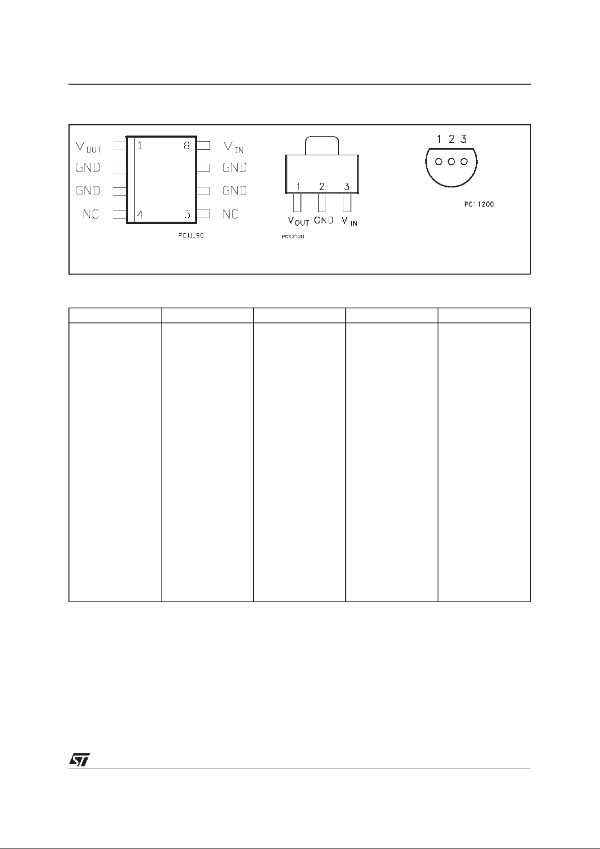
TESTCIRCUITS
THERMALDATA
Symbol Parameter SO-8 TO-92 SOT-89 Unit
R
thj-cas e
R
thj-amb
Thermal ResistanceJunction-case Max
Thermal ResistanceJunction-ambient Max2055 (*) 200
15
o
C/W
o
C/W
(*) Considering 6cm2of copper Board heat-sink
L78L00
2/19
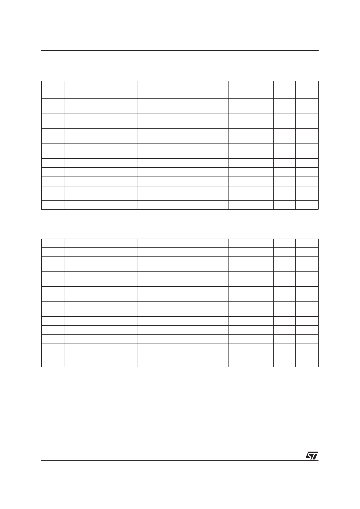
CONNECTION DIAGRAMAND ORDERING NUMBERS
(top view)
ORDERING NUMBERS
Type SO-8 TO-92 SOT-89 Output Voltage
L78L33AC
L78L33AB
L78L05C
L78L05AC
L78L05AB
L78L06C
L78L06AC
L78L06AB
L78L08C
L78L08AC
L78L08AB
L78L09C
L78L09AC
L78L09AB
L78L12C
L78L12AC
L78L12AB
L78L15C
L78L15AC
L78L15AB
L78L18C
L78L18AC
L78L18AB
L78L24C
L78L24AC
L78L24AB
L78L33ACD
L78L33ABD
L78L05CD
L78L05ACD
L78L05ABD
L78L06CD
L78L06ACD
L78L06ABD
L78L08CD
L78L08ACD
L78L08ABD
L78L09CD
L78L09ACD
L78L09ABD
L78L12CD
L78L12ACD
L78L12ABD
L78L15CD
L78L15ACD
L78L15ABD
L78L18CD
L78L18ACD
L78L18ABD
L78L24CD
L78L24ACD
L78L24ABD
L78L33ACZ
L78L33ABZ
L78L05CZ
L78L05ACZ
L78L05ABZ
L78L06CZ
L78L06ACZ
L78L06ABZ
L78L08CZ
L78L08ACZ
L78L08ABZ
L78L09CZ
L78L09ACZ
L78L09ABZ
L78L12CZ
L78L12ACZ
L78L12ABZ
L78L15CZ
L78L15ACZ
L78L15ABZ
L78L18CZ
L78L18ACZ
L78L18ABZ
L78L24CZ
L78L24ACZ
L78L24ABZ
L78L33ACU
L78L33ABU
L78L05ACU
L78L05ABU
L78L06ACU
L78L06ABU
L78L08ACU
L78L08ABU
L78L09ACU
L78L09ABU
L78L12ACU
L78L12ABU
L78L15ACU
L78L15ABU
L78L18ACU
L78L18ABU
L78L24ACU
L78L24ABU
3.3 V
3.3 V
5V
5V
5V
6V
6V
6V
8V
8V
8V
9V
9V
9V
12 V
12 V
12 V
15 V
15 V
15 V
18 V
18 V
18 V
24 V
24 V
24 V
SO-8 TO-92
pin 1 = V
OUT
pin 2 = GND
pin 3 = V
IN
BOTTOM VIEW
SOT-89
L78L00
3/19
ELECTRICALCHARACTERISTICS FOR L78L05
(refer to thetest circuits,T
j
= 0 to125oC,
V
i
= 10V, Io=40 mA, Ci= 0.33 µF, Co= 0.1 µF unless otherwisespecified)
Symbol Parameter Test Conditions Min. Typ. Max. Unit
V
o
OutputVoltage Tj=25oC 4.655.4V
V
o
OutputVoltage Io=1 to 40 mA Vi= 7 to 20 V
I
o
=1 to 70 mA Vi=10V
4.5
4.5
5.5
5.5
V
V
∆
V
o
LineRegulation Vi= 7 to 20 V Tj=25oC
V
i
= 8 to 20 V Tj=25oC
200
150
mV
mV
∆V
o
LoadRegulation Io=1 to 100mA Tj=25oC
I
o
=1 to 40 mA Tj=25oC
60
30
mV
mV
I
d
QuiescentCurrent Tj=25oC
T
j
= 125oC
6
5.5
mA
mA
∆I
d
QuiescentCurrent Change Io=1 to 40 mA 0.2 mA
∆I
d
QuiescentCurrent Change Vi= 8 to 20 V 1.5 mA
eN OutputNoise Voltage B = 10Hzto 100KHz T
j
=25oC40
µV
SVR Supply VoltageRejection I
o
=40 mA f = 120Hz Tj=25oC
V
i
= 8 to 18 V
40 49 dB
V
d
Dropout Voltage 1.7 V
ELECTRICALCHARACTERISTICS FOR L78L06(refer to the test circuits,Tj= 0 to125oC,
V
i
= 12V, Io=40 mA, Ci= 0.33 µF, Co= 0.1 µF unless otherwisespecified)
Symbol Parameter Test Conditions Min. Typ. Max. Unit
V
o
OutputVoltage Tj=25oC5.5266.48V
V
o
OutputVoltage Io=1 to 40 mA Vi= 8.5 to 20 V
I
o
=1 to 70 mA Vi=12V
5.4
5.4
6.6
6.6
V
V
∆V
o
LineRegulation Vi= 8.5 to 20 V Tj=25oC
V
i
= 9 to 20 V Tj=25oC
200
150
mV
mV
∆
V
o
LoadRegulation Io=1 to 100mA Tj=25oC
I
o
=1 to 40 mA Tj=25oC
60
30
mV
mV
I
d
QuiescentCurrent Tj=25oC
T
j
= 125oC
6
5.5
mA
mA
∆
I
d
QuiescentCurrent Change Io=1 to 40 mA 0.2 mA
∆
I
d
QuiescentCurrent Change Vi= 8 to 20 V 1.5 mA
eN OutputNoise Voltage B = 10Hzto 100KHz T
j
=25oC50
µ
V
SVR Supply VoltageRejection I
o
=40 mA f = 120Hz Tj=25oC
V
i
= 9 to 20 V
38 46 dB
V
d
Dropout Voltage 1.7 V
L78L00
4/19
ELECTRICALCHARACTERISTICS FOR L78L08
(refer to thetest circuits,T
j
= 0 to125oC,
V
i
= 14V, Io=40 mA, Ci= 0.33 µF, Co= 0.1 µF unless otherwisespecified)
Symbol Parameter Test Conditions Min. Typ. Max. Unit
V
o
OutputVoltage Tj=25oC7.3688.64V
V
o
OutputVoltage Io=1 to 40 mA Vi= 10.5 to23V
I
o
=1 to 70 mA Vi=14V
7.2
7.2
8.8
8.8
V
V
∆
V
o
LineRegulation Vi= 10.5 to 23V Tj=25oC
V
i
=11to23V Tj=25oC
200
150
mV
mV
∆V
o
LoadRegulation Io=1 to 100mA Tj=25oC
I
o
=1 to 40 mA Tj=25oC
80
40
mV
mV
I
d
QuiescentCurrent Tj=25oC
T
j
= 125oC
6
5.5
mA
mA
∆I
d
QuiescentCurrent Change Io=1 to 40 mA 0.2 mA
∆I
d
QuiescentCurrent Change Vi=11to23V 1.5 mA
eN OutputNoise Voltage B = 10Hzto 100KHz T
j
=25oC60
µV
SVR Supply VoltageRejection I
o
=40 mA f = 120Hz Tj=25oC
V
i
=12to23V
36 45 dB
V
d
Dropout Voltage 1.7 V
ELECTRICALCHARACTERISTICS FOR L78L09(refer to the test circuits,Tj= 0 to125oC,
V
i
= 15V, Io=40 mA, Ci= 0.33 µF, Co= 0.1 µF unless otherwisespecified)
Symbol Parameter Test Conditions Min. Typ. Max. Unit
V
o
OutputVoltage Tj=25oC8.2899.72V
V
o
OutputVoltage Io=1 to 40 mA Vi= 11.5 to23V
I
o
=1 to 70 mA Vi=15V
8.1
8.1
9.9
9.9
V
V
∆V
o
LineRegulation Vi= 11.5 to 23V Tj=25oC
V
i
=12to23V Tj=25oC
250
200
mV
mV
∆
V
o
LoadRegulation Io=1 to 100mA Tj=25oC
I
o
=1 to 40 mA Tj=25oC
80
40
mV
mV
I
d
Quiescent Current Tj=25oC
T
j
= 125oC
6
5.5
mA
mA
∆
I
d
Quiescent Current Change Io=1 to 40 mA 0.2 mA
∆
I
d
Quiescent Current Change Vi=12to23V 1.5 mA
eN OutputNoise Voltage B = 10Hzto 100KHz T
j
=25oC70
µ
V
SVR Supply VoltageRejection I
o
=40 mA f = 120Hz Tj=25oC
V
i
=12to23V
36 44 dB
V
d
Dropout Voltage 1.7 V
L78L00
5/19

ELECTRICALCHARACTERISTICS FOR L78L12
(refer to thetest circuits,T
j
= 0 to125oC,
V
i
= 19V, Io=40 mA, Ci= 0.33 µF, Co= 0.1 µF unless otherwisespecified)
Symbol Parameter Test Conditions Min. Typ. Max. Unit
V
o
OutputVoltage Tj=25oC 11.1 12 1 2. 9 V
V
o
OutputVoltage Io=1 to 40 mA Vi= 14.5 to27V
I
o
=1 to 70 mA Vi=19V
10.8
10.8
13.2
13.2
V
V
∆
V
o
LineRegulation Vi= 14.5 to 27V Tj=25oC
V
i
=16to27V Tj=25oC
250
200
mV
mV
∆V
o
LoadRegulation Io=1 to 100mA Tj=25oC
I
o
=1 to 40 mA Tj=25oC
100
50
mV
mV
I
d
Quiescent Current Tj=25oC
T
j
= 125oC
6.5
6
mA
mA
∆I
d
Quiescent Current Change Io=1 to 40 mA 0.2 mA
∆I
d
Quiescent Current Change Vi=16to27V 1.5 mA
eN OutputNoise Voltage B = 10Hzto 100KHz T
j
=25oC80
µV
SVR Supply VoltageRejection I
o
=40 mA f = 120Hz Tj=25oC
V
i
=15to25V
36 42 dB
V
d
Dropout Voltage 1.7 V
ELECTRICALCHARACTERISTICS FOR L78L15(refer to the test circuits,Tj= 0 to125oC,
V
i
= 23V, Io=40 mA, Ci= 0.33 µF, Co= 0.1 µF unless otherwisespecified)
Symbol Parameter Test Conditions Min. Typ. Max. Unit
V
o
OutputVoltage Tj=25oC 13.8 15 1 6. 2 V
V
o
OutputVoltage Io=1 to 40 mA Vi= 17.5 to30V
I
o
=1 to 70 mA Vi=23V
13.5
13.5
16.5
16.5
V
V
∆V
o
LineRegulation Vi= 17.5 to 30V Tj=25oC
V
i
=20to30V Tj=25oC
300
250
mV
mV
∆
V
o
LoadRegulation Io=1 to 100mA Tj=25oC
I
o
=1 to 40 mA Tj=25oC
150
75
mV
mV
I
d
Quiescent Current Tj=25oC
T
j
= 125oC
6.5
6
mA
mA
∆
I
d
Quiescent Current Change Io=1 to 40 mA 0.2 mA
∆
I
d
Quiescent Current Change Vi=20to30V 1.5 mA
eN OutputNoise Voltage B = 10Hzto 100KHz T
j
=25oC90
µ
V
SVR Supply VoltageRejection I
o
=40 mA f = 120Hz Tj=25oC
V
i
= 18.5 to 28.5V
33 39 dB
V
d
Dropout Voltage 1.7 V
L78L00
6/19

ELECTRICALCHARACTERISTICS FOR L78L18
(refer to thetest circuits,T
j
= 0 to125oC,
V
i
= 27V, Io=40 mA, Ci= 0.33 µF, Co= 0.1 µF unless otherwisespecified)
Symbol Parameter Test Conditions Min. Typ. Max. Unit
V
o
OutputVoltage Tj=25oC 16.6 18 1 9. 4 V
V
o
OutputVoltage Io=1 to 40 mA Vi=22to33V
I
o
=1 to 70 mA Vi=27V
16.2
16.2
19.8
19.8
V
V
∆
V
o
LineRegulation Vi=22to33V Tj=25oC
V
i
=22to33V Tj=25oC
320
270
mV
mV
∆V
o
LoadRegulation Io=1 to 100mA Tj=25oC
I
o
=1 to 40 mA Tj=25oC
170
85
mV
mV
I
d
Quiescent Current Tj=25oC
T
j
= 125oC
6.5
6
mA
mA
∆I
d
Quiescent Current Change Io=1 to 40 mA 0.2 mA
∆I
d
Quiescent Current Change Vi=23to33V 1.5 mA
eN OutputNoise Voltage B = 10Hzto 100KHz T
j
=25oC120
µV
SVR Supply VoltageRejection I
o
=40 mA f = 120Hz Tj=25oC
V
i
=23to33V
32 38 dB
V
d
Dropout Voltage 1.7 V
ELECTRICALCHARACTERISTICS FOR L78L24(refer to the test circuits,Tj= 0 to125oC,
V
i
= 33V, Io=40 mA, Ci= 0.33 µF, Co= 0.1 µF unless otherwisespecified)
Symbol Parameter Test Conditions Min. Typ. Max. Unit
V
o
OutputVoltage Tj=25oC 22.1 24 2 5. 9 V
V
o
OutputVoltage Io=1 to 40 mA Vi=27to38V
I
o
=1 to 70 mA Vi=33V
21.6
21.6
26.4
26.4
V
V
∆V
o
LineRegulation Vi=27to38V Tj=25oC
V
i
=28to38V Tj=25oC
350
300
mV
mV
∆
V
o
LoadRegulation Io=1 to 100mA Tj=25oC
I
o
=1 to 40 mA Tj=25oC
200
100
mV
mV
I
d
Quiescent Current Tj=25oC
T
j
= 125oC
6.5
6
mA
mA
∆
I
d
Quiescent Current Change Io=1 to 40 mA 0.2 mA
∆
I
d
Quiescent Current Change Vi=28to38V 1.5 mA
eN OutputNoise Voltage B = 10Hzto 100KHz T
j
=25oC200
µ
V
SVR Supply VoltageRejection I
o
=40 mA f = 120Hz Tj=25oC
V
i
=29to35V
30 37 dB
V
d
Dropout Voltage 1.7 V
L78L00
7/19

ELECTRICALCHARACTERISTICS FOR L78L33AB AND L78L33AC
(refer to the test circuits,V
i
=8.3V, Io= 40 mA, Ci= 0.33 µF,Co= 0.1 µF,
T
j
= 0 to 125oC for L78L33AC,Tj= -40to 125oC for L78L33AB,unlessotherwise specified)
Symbol Parameter Test Conditions Min. Typ. Max. Unit
V
o
OutputVoltage Tj=25oC 3.168 3.3 3.432 V
V
o
OutputVoltage Io=1 to 40 mA Vi= 5.3 to 20 V
I
o
=1 to 70 mA Vi= 8.3 V
3.135
3.135
3.465
3.465
V
V
∆
V
o
LineRegulation Vi= 5.3 to 20 V Tj=25oC
V
i
= 6.3 to 20 V Tj=25oC
150
100
mV
mV
∆V
o
LoadRegulation Io=1 to 100mA Tj=25oC
I
o
=1 to 40 mA Tj=25oC
60
30
mV
mV
I
d
Quiescent Current Tj=25oC
T
j
= 125oC
6
5.5
mA
mA
∆I
d
Quiescent Current Change Io=1 to 40 mA 0.1 mA
∆I
d
Quiescent Current Change Vi= 6.3 to 20 V 1.5 mA
eN OutputNoise Voltage B = 10Hzto 100KHz T
j
=25oC40
µV
SVR Supply VoltageRejection I
o
=40 mA f = 120Hz Tj=25oC
V
i
= 6.3 to 16.3 V
41 49 dB
V
d
Dropout Voltage 1.7 V
ELECTRICALCHARACTERISTICS FOR L78L05AB AND L78L05AC
(refer to the test circuits,V
i
=10V, Io= 40 mA, Ci= 0.33 µF, Co= 0.1 µF,
T
j
= 0 to 125oC for L78L05AC,Tj= -40to 125oC for L78L05AB,unlessotherwise specified)
Symbol Parameter Test Conditions Min. Typ. Max. Unit
V
o
OutputVoltage Tj=25oC 4.855.2V
V
o
OutputVoltage Io=1 to 40 mA Vi= 7 to 20 V
I
o
=1 to 70 mA Vi=10V
4.75
4.75
5.25
5.25
V
V
∆V
o
LineRegulation Vi= 7 to 20 V Tj=25oC
V
i
= 8 to 20 V Tj=25oC
150
100
mV
mV
∆
V
o
LoadRegulation Io=1 to 100mA Tj=25oC
I
o
=1 to 40 mA Tj=25oC
60
30
mV
mV
I
d
Quiescent Current Tj=25oC
T
j
= 125oC
6
5.5
mA
mA
∆
I
d
Quiescent Current Change Io=1 to 40 mA 0.1 mA
∆
I
d
Quiescent Current Change Vi= 8 to 20 V 1.5 mA
eN OutputNoise Voltage B = 10Hzto 100KHz T
j
=25oC40
µ
V
SVR Supply VoltageRejection I
o
=40 mA f = 120Hz Tj=25oC
V
i
= 8 to 18 V
41 49 dB
V
d
Dropout Voltage 1.7 V
L78L00
8/19

ELECTRICALCHARACTERISTICS FOR L78L06AB AND L78L06AC
(refer to the test circuits,V
i
=12V, Io= 40 mA, Ci= 0.33 µF, Co= 0.1 µF,
T
j
= 0 to 125oC for L78L06AC,Tj= -40to 125oC for L78L06AB, unless otherwise specified)
Symbol Parameter Test Conditions Min. Typ. Max. Unit
V
o
OutputVoltage Tj=25oC5.7666.24V
V
o
OutputVoltage Io=1 to 40 mA Vi= 8.5 to 20 V
I
o
=1 to 70 mA Vi=12V
5.7
5.7
6.3
6.3
V
V
∆
V
o
LineRegulation Vi= 8.5 to 20 V Tj=25oC
V
i
= 9 to 20 V Tj=25oC
150
100
mV
mV
∆V
o
LoadRegulation Io=1 to 100mA Tj=25oC
I
o
=1 to 40 mA Tj=25oC
60
30
mV
mV
I
d
Quiescent Current Tj=25oC
T
j
= 125oC
6
5.5
mA
mA
∆I
d
Quiescent Current Change Io=1 to 40 mA 0.1 mA
∆I
d
Quiescent Current Change Vi= 9 to 20 V 1.5 mA
eN OutputNoise Voltage B = 10Hzto 100KHz T
j
=25oC50
µV
SVR Supply VoltageRejection I
o
=40 mA f = 120Hz Tj=25oC
V
i
= 9 to 20 V
39 46 dB
V
d
Dropout Voltage 1.7 V
ELECTRICALCHARACTERISTICS FOR L78L08AB AND L78L08AC
(refer to the test circuits,V
i
=14V, Io= 40 mA, Ci= 0.33 µF, Co= 0.1 µF,
T
j
= 0 to 125oC for L78L08AC,Tj= -40to 125oC for L78L08AB,unlessotherwise specified)
Symbol Parameter Test Conditions Min. Typ. Max. Unit
V
o
OutputVoltage Tj=25oC7.6888.32V
V
o
OutputVoltage Io=1 to 40 mA Vi= 10.5 to23V
I
o
=1 to 70 mA Vi=14V
7.6
7.6
8.4
8.4
V
V
∆V
o
LineRegulation Vi= 10.5 to 23V Tj=25oC
V
i
=11to23V Tj=25oC
175
125
mV
mV
∆
V
o
LoadRegulation Io=1 to 100mA Tj=25oC
I
o
=1 to 40 mA Tj=25oC
80
40
mV
mV
I
d
Quiescent Current Tj=25oC
T
j
= 125oC
6
5.5
mA
mA
∆
I
d
Quiescent Current Change Io=1 to 40 mA 0.1 mA
∆
I
d
Quiescent Current Change Vi=11to23V 1.5 mA
eN OutputNoise Voltage B = 10Hzto 100KHz T
j
=25oC60
µ
V
SVR Supply VoltageRejection I
o
=40 mA f = 120Hz Tj=25oC
V
i
=12to23V
37 45 dB
V
d
Dropout Voltage 1.7 V
L78L00
9/19

ELECTRICALCHARACTERISTICS FOR L78L09AB AND L78L09AC
(refer to the test circuits,V
i
=15V, Io= 40 mA, Ci= 0.33 µF, Co= 0.1 µF,
T
j
= 0 to 125oC for L78L09AC,Tj= -40to 125oC for L78L09AB, unless otherwise specified)
Symbol Parameter Test Conditions Min. Typ. Max. Unit
V
o
OutputVoltage Tj=25oC8.6499.36V
V
o
OutputVoltage Io=1 to 40 mA Vi= 11.5 to23V
I
o
=1 to 70 mA Vi=15V
8.55
8.55
9.45
9.45
V
V
∆
V
o
LineRegulation Vi= 11.5 to 23V Tj=25oC
V
i
=12to23V Tj=25oC
225
150
mV
mV
∆V
o
LoadRegulation Io=1 to 100mA Tj=25oC
I
o
=1 to 40 mA Tj=25oC
80
40
mV
mV
I
d
Quiescent Current Tj=25oC
T
j
= 125oC
6
5.5
mA
mA
∆I
d
Quiescent Current Change Io=1 to 40 mA 0.1 mA
∆I
d
Quiescent Current Change Vi=12to23V 1.5 mA
eN OutputNoise Voltage B = 10Hzto 100KHz T
j
=25oC70
µV
SVR Supply VoltageRejection I
o
=40 mA f = 120Hz Tj=25oC
V
i
=12to23V
37 44 dB
V
d
Dropout Voltage 1.7 V
ELECTRICALCHARACTERISTICS FOR L78L12AB AND L78L12AC
(refer to the test circuits,V
i
=19V, Io= 40 mA, Ci= 0.33 µF, Co= 0.1 µF,
T
j
= 0 to 125oC for L78L12AC,Tj= -40to 125oC for L78L12AB,unlessotherwise specified)
Symbol Parameter Test Conditions Min. Typ. Max. Unit
V
o
OutputVoltage Tj=25oC 11.5 12 1 2. 5 V
V
o
OutputVoltage Io=1 to 40 mA Vi= 14.5 to27V
I
o
=1 to 70 mA Vi=19V
11.4
11.4
12.6
12.6
V
V
∆V
o
LineRegulation Vi= 14.5 to 27V Tj=25oC
V
i
=16to27V Tj=25oC
250
200
mV
mV
∆
V
o
LoadRegulation Io=1 to 100mA Tj=25oC
I
o
=1 to 40 mA Tj=25oC
100
50
mV
mV
I
d
Quiescent Current Tj=25oC
T
j
= 125oC
6.5
6
mA
mA
∆
I
d
Quiescent Current Change Io=1 to 40 mA 0.1 mA
∆
I
d
Quiescent Current Change Vi=16to27V 1.5 mA
eN OutputNoise Voltage B = 10Hzto 100KHz T
j
=25oC80
µ
V
SVR Supply VoltageRejection I
o
=40 mA f = 120Hz Tj=25oC
V
i
=15to25V
37 42 dB
V
d
Dropout Voltage 1.7 V
L78L00
10/19

ELECTRICALCHARACTERISTICS FOR L78L15AB AND L78L15AC
(refer to the test circuits,V
i
=23V, Io= 40 mA, Ci= 0.33 µF, Co= 0.1 µF,
T
j
= 0 to 125oC for L78L15AC,Tj= -40to 125oC for L78L15AB,unlessotherwise specified)
Symbol Parameter Test Conditions Min. Typ. Max. Unit
V
o
OutputVoltage Tj=25oC 14.4 15 1 5. 6 V
V
o
OutputVoltage Io=1 to 40 mA Vi= 17.5 to30V
I
o
=1 to 70 mA Vi=23V
14.25
14.25
15.75
15.75
V
V
∆
V
o
LineRegulation Vi= 17.5 to 30V Tj=25oC
V
i
=20to30V Tj=25oC
300
250
mV
mV
∆V
o
LoadRegulation Io=1 to 100mA Tj=25oC
I
o
=1 to 40 mA Tj=25oC
150
75
mV
mV
I
d
Quiescent Current Tj=25oC
T
j
= 125oC
6.5
6
mA
mA
∆I
d
Quiescent Current Change Io=1 to 40 mA 0.1 mA
∆I
d
Quiescent Current Change Vi=20to30V 1.5 mA
eN OutputNoise Voltage B = 10Hzto 100KHz T
j
=25oC90
µV
SVR Supply VoltageRejection I
o
=40 mA f = 120Hz Tj=25oC
V
i
= 18.5 to 28.5V
34 39 dB
V
d
Dropout Voltage 1.7 V
ELECTRICALCHARACTERISTICS FOR L78L18AB AND L78L18AC
(refer to the test circuits,V
i
=27V, Io= 40 mA, Ci= 0.33 µF, Co= 0.1 µF,
T
j
= 0 to 125oC for L78L18AC,Tj= -40to 125oC for L78L18AB,unlessotherwise specified)
Symbol Parameter Test Conditions Min. Typ. Max. Unit
V
o
OutputVoltage Tj=25oC 17.3 18 1 8. 7 V
V
o
OutputVoltage Io=1 to 40 mA Vi=22to33V
I
o
=1 to 70 mA Vi=27V
17.1
17.1
18.9
18.9
V
V
∆V
o
LineRegulation Vi=22to33V Tj=25oC
V
i
=22to33V Tj=25oC
320
270
mV
mV
∆
V
o
LoadRegulation Io=1 to 100mA Tj=25oC
I
o
=1 to 40 mA Tj=25oC
170
85
mV
mV
I
d
Quiescent Current Tj=25oC
T
j
= 125oC
6.5
6
mA
mA
∆
I
d
Quiescent Current Change Io=1 to 40 mA 0.1 mA
∆
I
d
Quiescent Current Change Vi=23to33V 1.5 mA
eN OutputNoise Voltage B = 10Hzto 100KHz T
j
=25oC120
µ
V
SVR Supply VoltageRejection I
o
=40 mA f = 120Hz Tj=25oC
V
i
=23to33V
33 38 dB
V
d
Dropout Voltage 1.7 V
L78L00
11/19

ELECTRICALCHARACTERISTICS FOR L78L24AB AND L78L24AC
(refer to the test circuits,V
i
=33V, Io= 40 mA, Ci= 0.33 µF, Co= 0.1 µF,
T
j
= 0 to 125oC for L78L24AC,Tj= -40to 125oC for L78L24AB,unlessotherwise specified)
Symbol Parameter Test Conditions Min. Typ. Max. Unit
V
o
OutputVoltage Tj=25oC 232425V
V
o
OutputVoltage Io=1 to 40 mA Vi=27to38V
I
o
=1 to 70 mA Vi=33V
22.8
22.8
25.2
25.2
V
V
∆
V
o
LineRegulation Vi=27to38V Tj=25oC
V
i
=28to38V Tj=25oC
350
300
mV
mV
∆V
o
LoadRegulation Io=1 to 100mA Tj=25oC
I
o
=1 to 40 mA Tj=25oC
200
100
mV
mV
I
d
Quiescent Current Tj=25oC
T
j
= 125oC
6.5
6
mA
mA
∆I
d
Quiescent Current Change Io=1 to 40 mA 0.1 mA
∆I
d
Quiescent Current Change Vi=28to38V 1.5 mA
eN OutputNoise Voltage B = 10Hzto 100KHz T
j
=25oC200
µV
SVR Supply VoltageRejection I
o
=40 mA f = 120Hz Tj=25oC
V
i
=29to35V
31 37 dB
V
d
Dropout Voltage 1.7 V
L78L00
12/19

Figure3 : L78L05/12/24Thermal Shutdown. Figure 4 : L78L05/12Quiescent Current vs
OutputCurrent
Figure5 :
L78L05 QuiescentCurrent vs Input
Voltage.
Figure6
: L78L05/12/24Output Characteristics.
Figure1:
L78L05/12Output Voltage vsAmbient
Temperature
Figure2 :
L78L05/12/24Load Characteristics.
L78L00
13/19

Figure9 : L78L00 Series Short Circuit Output
Current.
Figure7 :
L78L05/12/24Ripple Rejection.
Figure8 :
L78L05Dropout Characteristics.
TYPICALAPPLICATIONS:
Figure10: High OutputCurrent Short Circuit Protected
L78L00
14/19

Figure12 : Current Regulator.
Figure11 :
Output BoostCircuit.
Figure13:
AdjustableOutputRegulator
L78L00
15/19

DIM.
mm inch
MIN. TYP. MAX. MIN. TYP. MAX.
A 1.75 0.068
a1 0.1 0.25 0.003 0.009
a2 1.65 0.064
a3 0.65 0.85 0.025 0.033
b 0.35 0.48 0.013 0.018
b1 0.19 0.25 0.007 0.010
C 0.25 0.5 0.010 0.019
c1 45 (typ.)
D 4.8 5.0 0.188 0.196
E 5.8 6.2 0.228 0.244
e 1.27 0.050
e3 3.81 0.150
F 3.8 4.0 0.14 0.157
L 0.4 1.27 0.015 0.050
M 0.6 0.023
S 8 (max.)
0016023
SO-8 MECHANICAL DATA
L78L00
16/19

DIM.
mm mils
MIN. TYP. MAX. MIN. TYP. MAX.
A 1.4 1.6 55.1 63.0
B 0.44 0.56 17.3 22.0
B1 0.36 0.48 14.2 18.9
C 0.35 0.44 13.8 17.3
C1 0.35 0.44 13.8 17.3
D 4.4 4.6 173.2 181.1
D1 1.62 1.83 63.8 72.0
E 2.29 2.6 90.2 102.4
e 1.42 1.57 55.9 61.8
e1 2.92 3.07 115.0 120.9
H 3.94 4.25 155.1 167.3
L 0.89 1.2 35.0 47.2
P025H
SOT-89 MECHANICAL DATA
L78L00
17/19

DIM.
mm inch
MIN. TYP. MAX. MIN. TYP. MAX.
A 4.58 5.33 0.180 0.210
B 4.45 5.2 0.175 0.204
C 3.2 4.2 0.126 0.165
D 12.7 0.500
E 1.27 0.050
F 0.4 0.51 0.016 0.020
G 0.35 0.14
TO-92 MECHANICAL DATA
L78L00
18/19

Information furnished is believed to be accurate and reliable. However, STMicroelectronics assumes no responsibility for the consequences
of use of such information nor for any infringement of patents or other rights of third parties which may result from its use. No license is
granted by implication or otherwise under any patent or patent rights of STMicroelectronics. Specification mentioned in this publication are
subject tochange without notice. This publication supersedes and replaces all information previously supplied. STMicroelectronics products
are notauthorized for use as critical components in life support devices or systems without express written approval of STMicroelectronics.
The ST logo is a trademarkof STMicroelectronics
1999 STMicroelectronics – Printed in Italy – All Rights Reserved
STMicroelectronics GROUP OF COMPANIES
Australia - Brazil - Canada -China -France - Germany - Italy - Japan - Korea - Malaysia -Malta - Mexico - Morocco - The Netherlands -
Singapore -Spain - Sweden - Switzerland - Taiwan - Thailand - UnitedKingdom - U.S.A.
http://www.st.com
.
L78L00
19/19
 Loading...