

L7800
SERIES
POSITIVE VOLTAGE REGULATORS
November 1999
■ OUTPUT CURRENT UPTO1.5 A
■ OUTPUT VOLTAGESOF 5;5.2; 6;8; 8.5; 9;
12;15; 18; 24V
■ THERMAL OVERLOADPROTECTION
■ SHORTCIRCUIT PROTECTION
■ OUTPUT TRANSITIONSOAPROTECTION
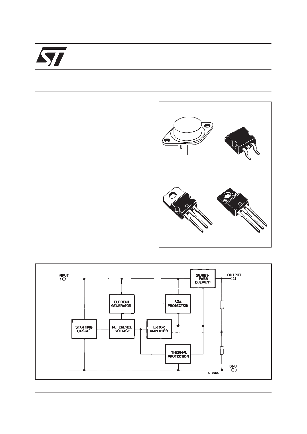
DESCRIPTION
The L7800 series of three-terminal positive
regulators is available in TO-220 ISOWATT220
TO-3 and D
2
PAK packages and several fixed
output voltages, making it useful in a wide range
of applications.Theseregulators can provide local
on-card regulation, eliminating the distribution
problems associated with single point regulation.
Each type employs internal current limiting,
thermal shut-down and safe area protection,
making it essentially indestructible. If adequate
heat sinking is provided,they can deliver over 1A
output current. Although designed primarily as
fixed voltage regulators, these devices can be
used with external components to obtain
adjustablevoltages and currents.
1
2
TO-3
TO-220 ISOWATT220
D2PAK
BLOCKDIAGRAM
1/25

CONNECTION DIAGRAM AND ORDERING NUMBERS(top view)
TO-220 & ISOWATT220 TO-3D2PAK
THERMALDATA
Symbol Parameter D2PAK TO-220 ISOWATT220 TO-3 Unit
R
thj-cas e
R
thj-amb
Thermal Resistance Junction-case Max
Thermal Resistance Junction-ambient Max
3
62.5
3
50
4
60
4
35
o
C/W
o
C/W
Type TO-220 D
2
PAK (*) ISOWATT220 TO-3 Output Voltage
L7805
L7805C
L7852C
L7806
L7806C
L7808
L7808C
L7885C
L7809C
L7812
L7812C
L7815
L7815C
L7818
L7818C
L7820
L7820C
L7824
L7824C
L7805CV
L7852CV
L7806CV
L7808CV
L7885CV
L7809CV
L7812CV
L7815CV
L7818CV
L7820CV
L7824CV
L7805CD2T
L7852CD2T
L7806CD2T
L7808CD2T
L7885CD2T
L7809CD2T
L7812CD2T
L7815CD2T
L7818CD2T
L7820CD2T
L7824CD2T
L7805CP
L7852CP
L7806CP
L7808CP
L7885CP
L7809CP
L7812CP
L7815CP
L7818CP
L7820CP
L7824CP
L7805T
L7805CT
L7852CT
L7806T
L7806CT
L7808T
L7808CT
L7885CT
L7809CT
L7812T
L7812CT
L7815T
L7815CT
L7818T
L7818CT
L7820T
L7820CT
L7824T
L7824CT
5V
5V
5.2V
6V
6V
8V
8V
8.5V
9V
12V
12V
15V
15V
18V
18V
20V
20V
24V
24V
(*) AVAILABLE IN TAPE AND REEL WITH ”-TR” SUFFIX
ABSOLUTE MAXIMUM RATINGS
Symbol Parameter Value Unit
V
i
DC InputVoltage(forVO= 5 to 18V)
(forV
O
= 20,24V)
35
40
V
V
I
o
OutputCurrent Internally limited
P
tot
PowerDissipation Internally limited
T
op
OperatingJunctionTemperatureRange (for L7800)
(for L7800C)
-55 to 150
0to150
o
C
o
C
T
stg
StorageTemperature Range -65 to 150
o
C
L7800
2/25
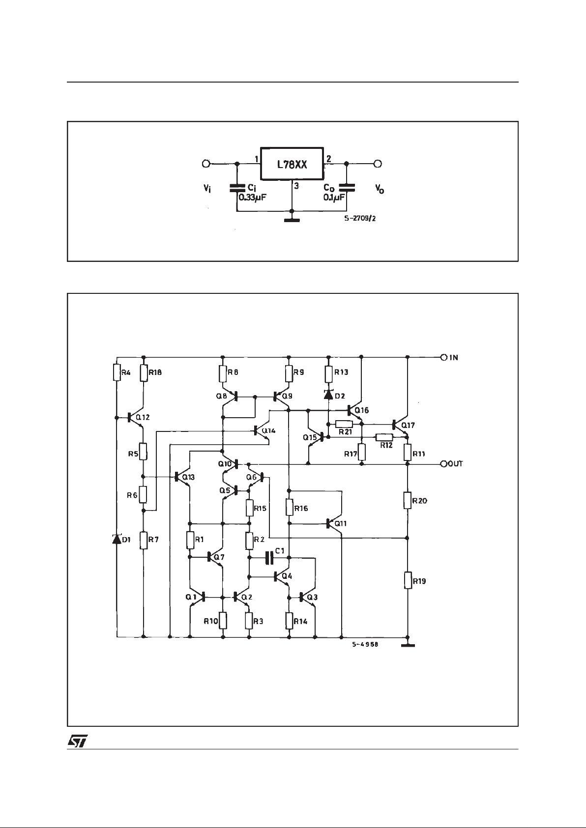
APPLICATION CIRCUIT
SCHEMATIC DIAGRAM
L7800
3/25
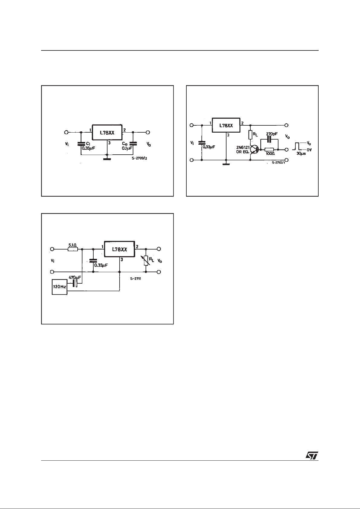
TESTCIRCUITS
Figure3 : RippleRejection.
Figure2 : Load Regulation.Figure1 : DC Parameter
L7800
4/25
ELECTRICALCHARACTERISTICS FOR L7806
(refer to the test circuits, T
j
= -55 to 150oC,
V
i
= 15V, Io=500 mA, Ci=0.33 µF, Co=0.1 µF unlessotherwisespecified)
Symbol Parameter Test Conditions Min. Typ. Max. Unit
V
o
OutputVoltage Tj=25oC5.7566.25V
V
o
OutputVoltage Io=5 mA to 1 A Po≤ 15W
V
i
= 9 to 21 V
5.65 6 6.35 V
∆
V
o
* LineRegulation Vi= 8 to 25 V Tj=25oC
V
i
= 9 to 13 V Tj=25oC
60
30
mV
mV
∆V
o
* LoadRegulation Io=5 to 1500 mA Tj=25oC
I
o
=250 to 750mA Tj=25oC
100
30
mV
mV
I
d
QuiescentCurrent Tj=25oC6mA
∆
I
d
QuiescentCurrentChange Io=5 to 1000 mA 0.5 mA
∆
I
d
QuiescentCurrentChange Vi= 9 to 25 V 0.8 mA
∆
V
o
∆
T
OutputVoltageDrift Io=5mA 0.7 mV/oC
eN OutputNoiseVoltage B = 10Hz to 100KHz T
j
=25oC40µV/V
O
SVR Supply Voltage Rejection Vi= 9 to 19 V f = 120Hz 65 dB
V
d
Dropout Voltage Io=1A Tj=25oC22.5V
R
o
OutputResistance f = 1 KHz 19 m
Ω
I
sc
ShortCircuitCurrent Vi=35V Tj=25oC0.751.2A
I
scp
ShortCircuitPeak Current Tj=25oC 1.3 2.2 3.3 A
ELECTRICALCHARACTERISTICS FOR L7805 (refer to the test circuits, Tj= -55 to 150oC,
V
i
= 10V, Io=500 mA, Ci=0.33 µF, Co=0.1 µF unlessotherwisespecified)
Symbol Parameter Test Conditions Min. Typ. Max. Unit
V
o
OutputVoltage Tj=25oC 4.855.2V
V
o
OutputVoltage Io=5 mA to 1 A P
o
≤
15W
V
i
= 8 to 20 V
4.65 5 5.35 V
∆
V
o
* LineRegulation Vi= 7 to 25 V Tj=25oC
V
i
= 8 to 12 V Tj=25oC
3
1
50
25
mV
mV
∆
V
o
* LoadRegulation Io=5 to 1500 mA Tj=25oC
I
o
=250 to 750mA Tj=25oC
100
25
mV
mV
I
d
QuiescentCurrent Tj=25oC6mA
∆I
d
QuiescentCurrentChange Io=5 to 1000 mA 0.5 mA
∆
I
d
QuiescentCurrentChange Vi= 8 to 25 V 0.8 mA
∆
V
o
∆
T
OutputVoltageDrift Io=5mA 0.6 mV/oC
eN OutputNoiseVoltage B = 10Hz to 100KHz T
j
=25oC40
µ
V/V
O
SVR Supply Voltage Rejection Vi= 8 to 18 V f = 120Hz 68 dB
V
d
Dropout Voltage Io=1A Tj=25oC22.5V
R
o
OutputResistance f = 1 KHz 17 mΩ
I
sc
ShortCircuitCurrent Vi=35V Tj=25oC0.751.2A
I
scp
ShortCircuitPeak Current Tj=25oC 1.3 2.2 3.3 A
* Load and line regulation are specified at constant junction temperature. Changes in Vodue to heating effects must be taken into account
separately. Pulce testing with low duty cycle is used.
L7800
5/25

ELECTRICALCHARACTERISTICS FOR L7812
(refer to the test circuits, T
j
= -55 to 150oC,
V
i
= 19V, Io=500 mA, Ci=0.33 µF, Co=0.1 µF unlessotherwisespecified)
Symbol Parameter Test Conditions Min. Typ. Max. Unit
V
o
OutputVoltage Tj=25oC 11.5 12 1 2.5 V
V
o
OutputVoltage Io=5 mA to 1 A Po≤ 15W
V
i
= 15.5to 27 V
11.4 12 12.6 V
∆
V
o
* LineRegulation Vi= 14.5to 30 V Tj=25oC
V
i
=16to22V Tj=25oC
120
60
mV
mV
∆V
o
* LoadRegulation Io=5 to 1500 mA Tj=25oC
I
o
=250 to 750mA Tj=25oC
100
60
mV
mV
I
d
QuiescentCurrent Tj=25oC6mA
∆
I
d
QuiescentCurrentChange Io=5 to 1000 mA 0.5 mA
∆
I
d
QuiescentCurrentChange Vi=15to30V 0.8 mA
∆
V
o
∆
T
OutputVoltageDrift Io=5mA 1.5 mV/oC
eN OutputNoiseVoltage B = 10Hzto 100KHz T
j
=25oC40µV/V
O
SVR Supply VoltageRejection Vi= 15 to 25 V f= 120 Hz 61 dB
V
d
Dropout Voltage Io=1A Tj=25oC22.5V
R
o
OutputResistance f = 1KHz 18 m
Ω
I
sc
ShortCircuitCurrent Vi=35V Tj=25oC0.751.2A
I
scp
ShortCircuitPeak Current Tj=25oC 1.3 2.2 3.3 A
ELECTRICALCHARACTERISTICS FOR L7808 (refer to the test circuits, Tj= -55 to 150oC,
V
i
= 14V, Io=500 mA, Ci=0.33 µF, Co=0.1 µF unlessotherwisespecified)
Symbol Parameter Test Conditions Min. Typ. Max. Unit
V
o
OutputVoltage Tj=25oC 7.788.3V
V
o
OutputVoltage Io=5 mA to 1 A P
o
≤
15W
V
i
= 11.5to 23 V
7.688.4V
∆
V
o
* LineRegulation Vi= 10.5to 25 V Tj=25oC
V
i
=11to17V Tj=25oC
80
40
mV
mV
∆
V
o
* LoadRegulation Io=5 to 1500 mA Tj=25oC
I
o
=250 to 750mA Tj=25oC
100
40
mV
mV
I
d
Quiescent Current Tj=25oC6mA
∆I
d
Quiescent CurrentChange Io=5 to 1000 mA 0.5 mA
∆
I
d
Quiescent CurrentChange Vi= 11.5to 25 V 0.8 mA
∆
V
o
∆
T
OutputVoltageDrift Io=5mA 1 mV/oC
eN OutputNoiseVoltage B = 10Hzto 100KHz T
j
=25oC40
µ
V/V
O
SVR Supply VoltageRejection Vi= 11.5to 21.5 V f =120 Hz 62 dB
V
d
Dropout Voltage Io=1A Tj=25oC22.5V
R
o
OutputResistance f = 1KHz 16 mΩ
I
sc
ShortCircuitCurrent Vi=35V Tj=25oC0.751.2A
I
scp
ShortCircuitPeak Current Tj=25oC 1.3 2.2 3.3 A
* Load and line regulation are specified at constant junction temperature. Changes in Vodue to heating effects must be taken into account
separately. Pulce testing with low duty cycle is used.
L7800
6/25

ELECTRICALCHARACTERISTICS FOR L7818
(refer to the test circuits, T
j
= -55 to 150oC,
V
i
= 26V, Io=500 mA, Ci=0.33 µF, Co=0.1 µF unlessotherwisespecified)
Symbol Parameter Test Conditions Min. Typ. Max. Unit
V
o
OutputVoltage Tj=25oC 17.3 18 1 8.7 V
V
o
OutputVoltage Io=5 mA to 1 A Po≤ 15W
V
i
=22to33V
17.1 18 18.9 V
∆
V
o
* LineRegulation Vi=21to33V Tj=25oC
V
i
=24to30V Tj=25oC
180
90
mV
mV
∆V
o
* LoadRegulation Io=5 to 1500 mA Tj=25oC
I
o
=250 to 750mA Tj=25oC
180
90
mV
mV
I
d
Quiescent Current Tj=25oC6mA
∆
I
d
Quiescent CurrentChange Io=5 to 1000 mA 0.5 mA
∆
I
d
Quiescent CurrentChange Vi=22to33V 0.8 mA
∆
V
o
∆
T
OutputVoltageDrift Io=5mA 2.3 mV/oC
eN OutputNoiseVoltage B = 10Hzto 100KHz T
j
=25oC40µV/V
O
SVR Supply VoltageRejection Vi= 22 to 32 V f= 120 Hz 59 dB
V
d
Dropout Voltage Io=1A Tj=25oC22.5V
R
o
OutputResistance f = 1KHz 22 m
Ω
I
sc
ShortCircuitCurrent Vi=35V Tj=25oC0.751.2A
I
scp
ShortCircuitPeak Current Tj=25oC 1.3 2.2 3.3 A
ELECTRICALCHARACTERISTICS FOR L7815 (refer to the test circuits, Tj= -55 to 150oC,
V
i
= 23V, Io=500 mA, Ci=0.33 µF, Co=0.1 µF unlessotherwisespecified)
Symbol Parameter Test Conditions Min. Typ. Max. Unit
V
o
OutputVoltage Tj=25oC 14.4 15 1 5.6 V
V
o
OutputVoltage Io=5 mA to 1 A P
o
≤
15W
V
i
= 18.5to 30 V
14.25 15 15.75 V
∆
V
o
* LineRegulation Vi= 17.5to 30 V Tj=25oC
V
i
=20to26V Tj=25oC
150
75
mV
mV
∆
V
o
* LoadRegulation Io=5 to 1500 mA Tj=25oC
I
o
=250 to 750mA Tj=25oC
150
75
mV
mV
I
d
Quiescent Current Tj=25oC6mA
∆I
d
Quiescent CurrentChange Io=5 to 1000 mA 0.5 mA
∆
I
d
Quiescent CurrentChange Vi= 18.5to 30 V 0.8 mA
∆
V
o
∆
T
OutputVoltageDrift Io=5mA 1.8 mV/oC
eN OutputNoiseVoltage B = 10Hzto 100KHz T
j
=25oC40
µ
V/V
O
SVR Supply VoltageRejection Vi= 18.5to 28.5 V f =120 Hz 60 dB
V
d
Dropout Voltage Io=1A Tj=25oC22.5V
R
o
OutputResistance f = 1KHz 19 mΩ
I
sc
ShortCircuitCurrent Vi=35V Tj=25oC0.751.2A
I
scp
ShortCircuitPeak Current Tj=25oC 1.3 2.2 3.3 A
* Load and line regulation are specified at constant junction temperature. Changes in Vodue to heating effects must be taken into account
separately. Pulce testing with low duty cycle is used.
L7800
7/25
ELECTRICALCHARACTERISTICS FOR L7824
(refer to the test circuits, T
j
= -55 to 150oC,
V
i
= 33V, Io=500 mA, Ci=0.33 µF, Co=0.1 µF unlessotherwisespecified)
Symbol Parameter Test Conditions Min. Typ. Max. Unit
V
o
OutputVoltage Tj=25oC 232425V
V
o
OutputVoltage Io=5 mA to 1 A Po≤ 15W
V
i
=28to38V
22.8 24 25.2 V
∆
V
o
* LineRegulation Vi=27to38V Tj=25oC
V
i
=30to36V Tj=25oC
240
120
mV
mV
∆V
o
* LoadRegulation Io=5 to 1500 mA Tj=25oC
I
o
=250 to 750mA Tj=25oC
240
120
mV
mV
I
d
Quiescent Current Tj=25oC6mA
∆
I
d
Quiescent CurrentChange Io=5 to 1000 mA 0.5 mA
∆
I
d
Quiescent CurrentChange Vi=28to38V 0.8 mA
∆
V
o
∆
T
OutputVoltageDrift Io=5mA 3 mV/oC
eN OutputNoiseVoltage B = 10Hzto 100KHz T
j
=25oC40µV/V
O
SVR Supply VoltageRejection Vi= 28 to 38 V f= 120 Hz 56 dB
V
d
Dropout Voltage Io=1A Tj=25oC22.5V
R
o
OutputResistance f = 1KHz 28 m
Ω
I
sc
ShortCircuitCurrent Vi=35V Tj=25oC0.751.2A
I
scp
ShortCircuitPeak Current Tj=25oC 1.3 2.2 3.3 A
ELECTRICALCHARACTERISTICS FOR L7820 (refer to the test circuits, Tj= -55 to 150oC,
V
i
= 28V, Io=500 mA, Ci=0.33 µF, Co=0.1 µF unlessotherwisespecified)
Symbol Parameter Test Conditions Min. Typ. Max. Unit
V
o
OutputVoltage Tj=25oC 19.2 20 2 0.8 V
V
o
OutputVoltage Io=5 mA to 1 A P
o
≤
15W
V
i
=24to35V
19 20 21 V
∆
V
o
* LineRegulation Vi= 22.5to 35 V Tj=25oC
V
i
=26to32V Tj=25oC
200
100
mV
mV
∆
V
o
* LoadRegulation Io=5 to 1500 mA Tj=25oC
I
o
=250 to 750mA Tj=25oC
200
100
mV
mV
I
d
Quiescent Current Tj=25oC6mA
∆I
d
Quiescent CurrentChange Io=5 to 1000 mA 0.5 mA
∆
I
d
Quiescent CurrentChange Vi=24to35V 0.8 mA
∆
V
o
∆
T
OutputVoltageDrift Io=5mA 2.5 mV/oC
eN OutputNoiseVoltage B = 10Hzto 100KHz T
j
=25oC40
µ
V/V
O
SVR Supply VoltageRejection Vi= 24 to 35 V f= 120 Hz 58 dB
V
d
Dropout Voltage Io=1A Tj=25oC22.5V
R
o
OutputResistance f = 1KHz 24 mΩ
I
sc
ShortCircuitCurrent Vi=35V Tj=25oC0.751.2A
I
scp
ShortCircuitPeak Current Tj=25oC 1.3 2.2 3.3 A
* Load and line regulation are specified at constant junction temperature. Changes in Vodue to heating effects must be taken into account
separately. Pulce testing with low duty cycle is used.
L7800
8/25

ELECTRICALCHARACTERISTICS FOR L7852C
(refer to the test circuits,T
j
= 0 to125oC, Vi= 10V,
I
o
= 500 mA, Ci= 0.33 µF, Co= 0.1 µF unless otherwise specified)
Symbol Parameter Test Conditions Min. Typ. Max. Unit
V
o
OutputVoltage Tj=25oC 5.0 5.2 5.4 V
V
o
OutputVoltage Io=5 mA to 1 A Po≤ 15W
V
i
= 8 to 20 V
4.95 5.2 5 . 45 V
∆
V
o
* LineRegulation Vi= 7 to 25 V Tj=25oC
V
i
= 8 to 12 V Tj=25oC
3
1
105
52
mV
mV
∆V
o
* LoadRegulation Io=5 to 1500 mA Tj=25oC
I
o
=250 to 750mA Tj=25oC
105
52
mV
mV
I
d
Quiescent Current Tj=25oC8mA
∆
I
d
Quiescent CurrentChange Io=5 to 1000 mA 0.5 mA
∆
I
d
Quiescent CurrentChange Vi= 7 to 25 V 1.3 mA
∆
V
o
∆
T
OutputVoltageDrift Io=5 mA -1.0 mV/oC
eN OutputNoiseVoltage B = 10Hzto 100KHz T
j
=25oC42µV
SVR Supply VoltageRejection V
i
= 8 to 18 V f = 120Hz 61 dB
V
d
Dropout Voltage Io=1A Tj=25oC2V
R
o
OutputResistance f = 1KHz 17 m
Ω
I
sc
ShortCircuitCurrent Vi=35V Tj=25oC750mA
I
scp
ShortCircuitPeak Current Tj=25oC2.2A
ELECTRICALCHARACTERISTICS FOR L7805C (refer to the test circuits, Tj= 0 to125oC,
V
i
= 10V, Io=500 mA, Ci=0.33 µF, Co=0.1 µF unlessotherwisespecified)
Symbol Parameter Test Conditions Min. Typ. Max. Unit
V
o
OutputVoltage Tj=25oC 4.855.2V
V
o
OutputVoltage Io=5 mA to 1 A P
o
≤
15W
V
i
= 7 to 20 V
4.75 5 5.25 V
∆
V
o
* LineRegulation Vi= 7 to 25 V Tj=25oC
V
i
= 8 to 12 V Tj=25oC
3
1
100
50
mV
mV
∆
V
o
* LoadRegulation Io=5 to 1500 mA Tj=25oC
I
o
=250 to 750mA Tj=25oC
100
50
mV
mV
I
d
Quiescent Current Tj=25oC8mA
∆I
d
Quiescent CurrentChange Io=5 to 1000 mA 0.5 mA
∆
I
d
Quiescent CurrentChange Vi= 7 to 25 V 0.8 mA
∆
V
o
∆
T
OutputVoltageDrift Io=5 mA -1.1 mV/oC
eN OutputNoiseVoltage B = 10Hzto 100KHz T
j
=25oC40
µ
V
SVR Supply VoltageRejection V
i
= 8 to 18 V f = 120Hz 62 dB
V
d
Dropout Voltage Io=1A Tj=25oC2V
R
o
OutputResistance f = 1KHz 17 mΩ
I
sc
ShortCircuitCurrent Vi=35V Tj=25oC750mA
I
scp
ShortCircuitPeak Current Tj=25oC2.2A
* Load and line regulation are specified at constant junction temperature. Changes in Vodue to heating effects must be taken into account
separately. Pulce testing with low duty cycle is used.
L7800
9/25

ELECTRICALCHARACTERISTICS FOR L7808C
(refer to the test circuits,T
j
= 0 to125oC, Vi= 14V,
I
o
= 500 mA, Ci= 0.33 µF, Co= 0.1 µF unless otherwise specified)
Symbol Parameter Test Conditions Min. Typ. Max. Unit
V
o
OutputVoltage Tj=25oC 7.788.3V
V
o
OutputVoltage Io=5 mA to 1 A Po≤ 15W
V
i
= 10.5to 25 V
7.688.4V
∆
V
o
* LineRegulation Vi= 10.5to 25 V Tj=25oC
V
i
=11to17V Tj=25oC
160
80
mV
mV
∆V
o
* LoadRegulation Io=5 to 1500 mA Tj=25oC
I
o
=250 to 750mA Tj=25oC
160
80
mV
mV
I
d
Quiescent Current Tj=25oC8mA
∆
I
d
Quiescent CurrentChange Io=5 to 1000 mA 0.5 mA
∆
I
d
Quiescent CurrentChange Vi= 10.5to 25 V 1 mA
∆
V
o
∆
T
OutputVoltageDrift Io=5 mA -0.8 mV/oC
eN OutputNoiseVoltage B = 10Hzto 100KHz T
j
=25oC52µV
SVR Supply VoltageRejection V
i
= 11.5to 21.5 V f =120 Hz 56 dB
V
d
Dropout Voltage Io=1A Tj=25oC2V
R
o
OutputResistance f = 1KHz 16 m
Ω
I
sc
ShortCircuitCurrent Vi=35V Tj=25oC450mA
I
scp
ShortCircuitPeak Current Tj=25oC2.2A
ELECTRICALCHARACTERISTICS FOR L7806C (refer to the test circuits, Tj= 0 to125oC,
V
i
= 11V, Io=500 mA, Ci=0.33 µF, Co=0.1 µF unlessotherwisespecified)
Symbol Parameter Test Conditions Min. Typ. Max. Unit
V
o
OutputVoltage Tj=25oC5.7566.25V
V
o
OutputVoltage Io=5 mA to 1 A P
o
≤
15W
V
i
= 8 to 21 V
5.766.3V
∆
V
o
* LineRegulation Vi= 8 to 25 V Tj=25oC
V
i
= 9 to 13 V Tj=25oC
120
60
mV
mV
∆
V
o
* LoadRegulation Io=5 to 1500 mA Tj=25oC
I
o
=250 to 750mA Tj=25oC
120
60
mV
mV
I
d
Quiescent Current Tj=25oC8mA
∆I
d
Quiescent CurrentChange Io=5 to 1000 mA 0.5 mA
∆
I
d
Quiescent CurrentChange Vi= 8 to 25 V 1.3 mA
∆
V
o
∆
T
OutputVoltageDrift Io=5 mA -0.8 mV/oC
eN OutputNoiseVoltage B = 10Hzto 100KHz T
j
=25oC45
µ
V
SVR Supply VoltageRejection V
i
= 9 to 19 V f = 120Hz 59 dB
V
d
Dropout Voltage Io=1A Tj=25oC2V
R
o
OutputResistance f = 1KHz 19 mΩ
I
sc
ShortCircuitCurrent Vi=35V Tj=25oC550mA
I
scp
ShortCircuitPeak Current Tj=25oC2.2A
* Load and line regulation are specified at constant junction temperature. Changes in Vodue to heating effects must be taken into account
separately. Pulce testing with low duty cycle is used.
L7800
10/25

ELECTRICALCHARACTERISTICS FOR L7809C
(refer to the test circuits,T
j
= 0 to125oC, Vi= 15V,
I
o
= 500 mA, Ci= 0.33 µF, Co= 0.1 µF unless otherwise specified)
Symbol Parameter Test Conditions Min. Typ. Max. Unit
V
o
OutputVoltage Tj=25oC8.6599.35V
V
o
OutputVoltage Io=5 mA to 1 A Po≤ 15W
V
i
= 11.5to 26 V
8.55 9 9.45 V
∆
V
o
* LineRegulation Vi= 11.5to 26 V Tj=25oC
V
i
=12to18V Tj=25oC
180
90
mV
mV
∆V
o
* LoadRegulation Io=5 to 1500 mA Tj=25oC
I
o
=250 to 750mA Tj=25oC
180
90
mV
mV
I
d
Quiescent Current Tj=25oC8mA
∆
I
d
Quiescent CurrentChange Io=5 to 1000 mA 0.5 mA
∆
I
d
Quiescent CurrentChange Vi= 11.5to 26 V 1 mA
∆
V
o
∆
T
OutputVoltageDrift Io=5 mA -1.0 mV/oC
eN OutputNoiseVoltage B = 10Hzto 100KHz T
j
=25oC70µV
SVR Supply VoltageRejection V
i
= 12 to 23 V f= 120 Hz 55 dB
V
d
Dropout Voltage Io=1A Tj=25oC2V
R
o
OutputResistance f = 1KHz 17 m
Ω
I
sc
ShortCircuitCurrent Vi=35V Tj=25oC400mA
I
scp
ShortCircuitPeak Current Tj=25oC2.2A
ELECTRICALCHARACTERISTICS FOR L7885C (refer to the test circuits, Tj= 0 to125oC, Vi=
14.5V,I
o
= 500 mA, Ci= 0.33 µF, Co= 0.1 µF unless otherwise specified)
Symbol Parameter Test Conditions Min. Typ. Max. Unit
V
o
OutputVoltage Tj=25oC 8.2 8.5 8.8 V
V
o
OutputVoltage Io=5 mA to 1 A P
o
≤
15W
V
i
=11to26V
8.1 8.5 8.9 V
∆
V
o
* LineRegulation Vi=11to27V Tj=25oC
V
i
= 11.5to 17.5 V Tj=25oC
160
80
mV
mV
∆
V
o
* LoadRegulation Io=5 to 1500 mA Tj=25oC
I
o
=250 to 750mA Tj=25oC
160
80
mV
mV
I
d
Quiescent Current Tj=25oC8mA
∆I
d
Quiescent CurrentChange Io=5 to 1000 mA 0.5 mA
∆
I
d
Quiescent CurrentChange Vi=11to27V 1 mA
∆
V
o
∆
T
OutputVoltageDrift Io=5 mA -0.8 mV/oC
eN OutputNoiseVoltage B = 10Hzto 100KHz T
j
=25oC55
µ
V
SVR Supply VoltageRejection V
i
= 12 to 22 V f= 120 Hz 56 dB
V
d
Dropout Voltage Io=1A Tj=25oC2V
R
o
OutputResistance f = 1KHz 16 mΩ
I
sc
ShortCircuitCurrent Vi=35V Tj=25oC450mA
I
scp
ShortCircuitPeak Current Tj=25oC2.2A
* Load and line regulation are specified at constant junction temperature. Changes in Vodue to heating effects must be taken into account
separately. Pulce testing with low duty cycle is used.
L7800
11/25

ELECTRICALCHARACTERISTICS FOR L7815C
(refer to the test circuits,T
j
= 0 to125oC, Vi= 23V,
I
o
= 500 mA, Ci= 0.33 µF, Co= 0.1 µF unless otherwise specified)
Symbol Parameter Test Conditions Min. Typ. Max. Unit
V
o
OutputVoltage Tj=25oC 14.4 15 1 5.6 V
V
o
OutputVoltage Io=5 mA to 1 A Po≤ 15W
V
i
= 17.5to 30 V
14.25 15 15.75 V
∆
V
o
* LineRegulation Vi= 17.5to 30 V Tj=25oC
V
i
=20to26V Tj=25oC
300
150
mV
mV
∆V
o
* LoadRegulation Io=5 to 1500 mA Tj=25oC
I
o
=250 to 750mA Tj=25oC
300
150
mV
mV
I
d
Quiescent Current Tj=25oC8mA
∆
I
d
Quiescent CurrentChange Io=5 to 1000 mA 0.5 mA
∆
I
d
Quiescent CurrentChange Vi= 17.5to 30 V 1 mA
∆
V
o
∆
T
OutputVoltageDrift Io=5 mA -1 mV/oC
eN OutputNoiseVoltage B = 10Hzto 100KHz T
j
=25oC90µV
SVR Supply VoltageRejection V
i
= 18.5to 28.5 V f =120 Hz 54 dB
V
d
Dropout Voltage Io=1A Tj=25oC2V
R
o
OutputResistance f = 1KHz 19 m
Ω
I
sc
ShortCircuitCurrent Vi=35V Tj=25oC230mA
I
scp
ShortCircuitPeak Current Tj=25oC2.1A
ELECTRICALCHARACTERISTICS FOR L7812C (refer to the test circuits, Tj= 0 to125oC, Vi= 19V,
I
o
= 500 mA, Ci= 0.33 µF, Co= 0.1 µF unless otherwise specified)
Symbol Parameter Test Conditions Min. Typ. Max. Unit
V
o
OutputVoltage Tj=25oC 11.5 12 1 2.5 V
V
o
OutputVoltage Io=5 mA to 1 A P
o
≤
15W
V
i
= 14.5to 27 V
11.4 12 12.6 V
∆
V
o
* LineRegulation Vi= 14.5to 30 V Tj=25oC
V
i
=16to22V Tj=25oC
240
120
mV
mV
∆
V
o
* LoadRegulation Io=5 to 1500 mA Tj=25oC
I
o
=250 to 750mA Tj=25oC
240
120
mV
mV
I
d
Quiescent Current Tj=25oC8mA
∆I
d
Quiescent CurrentChange Io=5 to 1000 mA 0.5 mA
∆
I
d
Quiescent CurrentChange Vi= 14.5to 30 V 1 mA
∆
V
o
∆
T
OutputVoltageDrift Io=5 mA -1 mV/oC
eN OutputNoiseVoltage B = 10Hzto 100KHz T
j
=25oC75
µ
V
SVR Supply VoltageRejection V
i
= 15 to 25 V f= 120 Hz 55 dB
V
d
Dropout Voltage Io=1A Tj=25oC2V
R
o
OutputResistance f = 1KHz 18 mΩ
I
sc
ShortCircuitCurrent Vi=35V Tj=25oC350mA
I
scp
ShortCircuitPeak Current Tj=25oC2.2A
* Load and line regulation are specified at constant junction temperature. Changes in Vodue to heating effects must be taken into account
separately. Pulce testing with low duty cycle is used.
L7800
12/25

ELECTRICALCHARACTERISTICS FOR L7820C
(refer to the test circuits,T
j
= 0 to125oC, Vi= 28V,
I
o
= 500 mA, Ci= 0.33 µF, Co= 0.1 µF unless otherwise specified)
Symbol Parameter Test Conditions Min. Typ. Max. Unit
V
o
OutputVoltage Tj=25oC 19.2 20 2 0.8 V
V
o
OutputVoltage Io=5 mA to 1 A Po≤ 15W
V
i
=23to35V
19 20 21 V
∆
V
o
* LineRegulation Vi= 22.5to 35 V Tj=25oC
V
i
=26to32V Tj=25oC
400
200
mV
mV
∆V
o
* LoadRegulation Io=5 to 1500 mA Tj=25oC
I
o
=250 to 750mA Tj=25oC
400
200
mV
mV
I
d
Quiescent Current Tj=25oC8mA
∆
I
d
Quiescent CurrentChange Io=5 to 1000 mA 0.5 mA
∆
I
d
Quiescent CurrentChange Vi=23to35V 1 mA
∆
V
o
∆
T
OutputVoltageDrift Io=5 mA -1 mV/oC
eN OutputNoiseVoltage B = 10Hzto 100KHz T
j
=25oC150µV
SVR Supply VoltageRejection V
i
= 24 to 35 V f= 120 Hz 52 dB
V
d
Dropout Voltage Io=1A Tj=25oC2V
R
o
OutputResistance f = 1KHz 24 m
Ω
I
sc
ShortCircuitCurrent Vi=35V Tj=25oC180mA
I
scp
ShortCircuitPeak Current Tj=25oC2.1A
ELECTRICALCHARACTERISTICS FOR L7818C (refer to the test circuits, Tj= 0 to125oC, Vi= 26V,
I
o
= 500 mA, Ci= 0.33 µF, Co= 0.1 µF unless otherwise specified)
Symbol Parameter Test Conditions Min. Typ. Max. Unit
V
o
OutputVoltage Tj=25oC 17.3 18 1 8.7 V
V
o
OutputVoltage Io=5 mA to 1 A P
o
≤
15W
V
i
=21to33V
17.1 18 18.9 V
∆
V
o
* LineRegulation Vi=21to33V Tj=25oC
V
i
=24to30V Tj=25oC
360
180
mV
mV
∆
V
o
* LoadRegulation Io=5 to 1500 mA Tj=25oC
I
o
=250 to 750mA Tj=25oC
360
180
mV
mV
I
d
Quiescent Current Tj=25oC8mA
∆I
d
Quiescent CurrentChange Io=5 to 1000 mA 0.5 mA
∆
I
d
Quiescent CurrentChange Vi=21to33V 1 mA
∆
V
o
∆
T
OutputVoltageDrift Io=5 mA -1 mV/oC
eN OutputNoiseVoltage B = 10Hzto 100KHz T
j
=25oC110
µ
V
SVR Supply VoltageRejection V
i
= 22 to 32 V f= 120 Hz 53 dB
V
d
Dropout Voltage Io=1A Tj=25oC2V
R
o
OutputResistance f = 1KHz 22 mΩ
I
sc
ShortCircuitCurrent Vi=35V Tj=25oC200mA
I
scp
ShortCircuitPeak Current Tj=25oC2.1A
* Load and line regulation are specified at constant junction temperature. Changes in Vodue to heating effects must be taken into account
separately. Pulce testing with low duty cycle is used.
L7800
13/25

* Load and line regulation are specified at constant junction temperature. Changes in Vodue to heating effects must be taken into account
separately. Pulce testing with low duty cycle is used.
ELECTRICALCHARACTERISTICS FOR L7824C (refer to the test circuits, Tj= 0 to125oC, Vi= 33V,
I
o
= 500 mA, Ci= 0.33 µF, Co= 0.1 µF unless otherwise specified)
Symbol Parameter Test Conditions Min. Typ. Max. Unit
V
o
OutputVoltage Tj=25oC 232425V
V
o
OutputVoltage Io=5 mA to 1 A Po≤ 15W
V
i
=27to38V
22.8 24 25.2 V
∆
V
o
* LineRegulation Vi=27to38V Tj=25oC
V
i
=30to36V Tj=25oC
480
240
mV
mV
∆V
o
* LoadRegulation Io=5 to 1500 mA Tj=25oC
I
o
=250 to 750mA Tj=25oC
480
240
mV
mV
I
d
Quiescent Current Tj=25oC8mA
∆I
d
Quiescent CurrentChange Io=5 to 1000 mA 0.5 mA
∆I
d
Quiescent CurrentChange Vi=27to38V 1 mA
∆
V
o
∆
T
OutputVoltageDrift Io=5 mA -1.5 mV/oC
eN OutputNoiseVoltage B = 10Hzto 100KHz T
j
=25oC170
µ
V
SVR Supply VoltageRejection V
i
= 28 to 38 V f= 120 Hz 50 dB
V
d
Dropout Voltage Io=1A Tj=25oC2V
R
o
OutputResistance f = 1KHz 28 mΩ
I
sc
ShortCircuitCurrent Vi=35V Tj=25oC150mA
I
scp
ShortCircuitPeak Current Tj=25oC2.1A
L7800
14/25

Figure8 :
OutputImpedance vs.Frequency.
Figure9 :
QuiescentCurrentvs. Junction
Temperature.
Figure4 : DropoutVoltagevs. Junction
Temperature.
Figure5 : PeakOutput Currentvs. Input/output
DifferentialVoltage.
Figure6 :
SupplyVoltage Rejectionvs.
Frequency.
Figure7 :
OutputVoltage vs. Junction
Temperature.
L7800
15/25

Figure12 : QuiescentCurrent vs. Input
Voltage.
Figure13 :
Fixed Output Regulator.
Figure14 :
CurrentRegulator.
Figure10 :
Load TransientResponse.
Figure11 :
Line TransientResponse.
NOTE:
1. To specify anoutput voltage, substitute voltage value for ”XX”.
2. Although no output capacitor is need for stability, it does
improve transient response.
3. Required if cregulator is locate an appreciable distance from
power supply filter.
I
O
=
V
XX
R
1
+
I
d
L7800
16/25

Figure 15 :
Circuitfor IncreasingOutput
Voltage.
Figure 16 :
AdjustableOutput Regulator
(7 to 30V).
Figure 17 :
0.5 to 10V Regulator.
Figure 18 :
High CurrentVoltageRegulator.
I
R1
≥
5I
d
VO=
V
XX
(1+
R
2
R
1
)+
IdR
2
VO =
V
XX
R
4
R
1
R1=
V
BEQ
1
I
REQ
−
I
Q
1
β
Q
1
IO=
I
REG
+
Q
1
(
I
REG
−
V
BEQ
1
R
1
)
L7800
17/25

Figure19 :
High OutputCurrentwith Short
CircuitProtection.
Figure20 :
TrackingVoltage Regulator.
Figure21 :
Split PowerSupply(± 15V – 1A).
Figure22 :
NegativeOutput Voltage Circuit.
Figure23 :
Switching Regulator.
Figure24 :
High InputVoltage Circuit.
VIN=Vi-(VZ+VBE)
* Against potential latch-up problems.
R
SC
=
V
BEQ
2
I
SC
L7800
18/25

Figure27 :
High Input and OutputVoltage.
Figure28 :
ReducingPower Dissipation with
Dr opping Resistor.
Figure29 : RemoteShutdown.
Figure25 :
High Input Voltage Circuit.
Figure26 :
High OutputVoltage Regulator.
VO=VXX+V
Z1
R=
V
i(min
)
−
V
XX
−
V
DROP(max
)
I
O(max
)
+
I
d(max
)
L7800
19/25

Figure30 :
Power AM Modulator(unity voltage
gain,I
o
< 1A).
Figure31 :
AdjustableOutput Voltagewith
TemperatureCompensation.
NOTE: The circuit performs well up to 100KHz NOTE: Q2is connected as a diode in order to compensate the
variation of the Q
1VBE
with the temperature. C allows a slow rise-
time of the V
o
Figure32 :
Light Controllers(V
o min=Vxx+VBE
).
Figure33 : ProtectionagainstInput Short-circuit
withHigh CapacitanceLoads.
Application with high capacitance loads and an output voltage
greater than 6 volts need an external diode (see fig.33) to protect
the deviceagainst input short circuit. In this case the input voltage
falls rapidly while the output voltage decrease slowly. The
capacitance dischrges by means of the Base-Emitter junction of
the series pass transistor in the regulator. If the energy is
sufficently high, the transistor may be destroyed. The external
diode by-passes the current from the IC toground.
V
O
fallswhen the light goes up
V
O
rises when the lightgoes up
V
O
=
V
XX
(
1
+
R
2
R
1
)+
V
BE
L7800
20/25

DIM.
mm inch
MIN. TYP. MAX. MIN. TYP. MAX.
A 11.7 0.460
B 0.96 1.10 0.037 0.043
C 1.70 0.066
D 8.7 0.342
E 20.0 0.787
G 10.9 0.429
N 16.9 0.665
P 26.2 1.031
R 3.88 4.09 0.152 0.161
U 39.50 1.555
V 30.10 1.185
E
B
R
C
DA
P
G
N
V
U
O
P003N
TO-3 (R) MECHANICAL DATA
L7800
21/25

DIM.
mm inch
MIN. TYP. MAX. MIN. TYP. MAX.
A 4.40 4.60 0.173 0.181
C 1.23 1.32 0.048 0.051
D 2.40 2.72 0.094 0.107
D1 1.27 0.050
E 0.49 0.70 0.019 0.027
F 0.61 0.88 0.024 0.034
F1 1.14 1.70 0.044 0.067
F2 1.14 1.70 0.044 0.067
G 4.95 5.15 0.194 0.203
G1 2.4 2.7 0.094 0.106
H2 10.0 10.40 0.393 0.409
L2 16.4 0.645
L4 13.0 14.0 0.511 0.551
L5 2.65 2.95 0.104 0.116
L6 15.25 15.75 0.600 0.620
L7 6.2 6.6 0.244 0.260
L9 3.5 3.93 0.137 0.154
DIA. 3.75 3.85 0.147 0.151
L6
A
C
D
E
D1
F
G
L7
L2
Dia.
F1
L5
L4
H2
L9
F2
G1
TO-220 MECHANICAL DATA
P011C
L7800
22/25

DIM.
mm inch
MIN. TYP. MAX. MIN. TYP. MAX.
A 4.4 4.6 0.173 0.181
B 2.5 2.7 0.098 0.106
D 2.5 2.75 0.098 0.108
E 0.4 0.7 0.015 0.027
F 0.75 1 0.030 0.039
F1 1.15 1.7 0.045 0.067
F2 1.15 1.7 0.045 0.067
G 4.95 5.2 0.195 0.204
G1 2.4 2.7 0.094 0.106
H 10 10.4 0.393 0.409
L2 16 0.630
L3 28.6 30.6 1.126 1.204
L4 9.8 10.6 0.385 0.417
L6 15.9 16.4 0.626 0.645
L7 9 9.3 0.354 0.366
Ø 3 3.2 0.118 0.126
L2
A
B
D
E
H
G
L6
¯
F
L3
G1
123
F2
F1
L7
L4
ISOWATT220MECHANICAL DATA
P011G
L7800
23/25

DIM.
mm inch
MIN. TYP. MAX. MIN. TYP. MAX.
A 4.4 4.6 0.173 0.181
A1 2.49 2.69 0.098 0.106
B 0.7 0.93 0.027 0.036
B2 1.14 1.7 0.044 0.067
C 0.45 0.6 0.017 0.023
C2 1.23 1.36 0.048 0.053
D 8.95 9.35 0.352 0.368
E 10 10.4 0.393 0.409
G 4.88 5.28 0.192 0.208
L 15 15.85 0.590 0.624
L2 1.27 1.4 0.050 0.055
L3 1.4 1.75 0.055 0.068
L2
L3
L
B2
B
G
E
A
C2
D
C
A1
DETAIL”A”
DETAIL”A”
A2
P011P6/F
TO-263 (D2PAK) MECHANICALDATA
L7800
24/25

Information furnished isbelieved tobe accurate andreliable. However, STMicroelectronics assumes no responsibility for the consequences
of use of such information nor for any infringement of patents or other rights of third parties which may result from its use. No license is
granted by implication or otherwise under any patent or patent rights of STMicroelectronics. Specification mentioned in this publication are
subject tochange without notice. Thispublication supersedes and replaces all information previously supplied. STMicroelectronics products
are not authorized for use as critical components in life support devices or systems withoutexpress written approval of STMicroelectronics.
The ST logo is a registeredtrademark of STMicroelectronics
1999 STMicroelectronics – Printed in Italy – AllRightsReserved
STMicroelectronics GROUP OF COMPANIES
Australia - Brazil - China - Finland -France - Germany - Hong Kong - India - Italy- Japan - Malaysia -Malta - Morocco
Singapore - Spain- Sweden - Switzerland - United Kingdom - U.S.A.
http://www.st.com
.
L7800
25/25
 Loading...