

SGS Thomson Microelectronics L7824ABV, L7820ACV, L7824ACV, L7820ABV, L7818ACV Datasheet
...
L7800AB/AC
SERIES
PRECISION 1A REGULATORS
November 1999
■ OUTPUT CURRENT INEXCESSOF1 A
■
OUTPUT VOLTAGESOF 5;6; 8; 9; 12; 15; 18;
20;24V
■
THERMAL OVERLOADPROTECTION
■ OUTPUT TRANSITIONSOAPROTECTION
■ 2%OUTPUTVOLTAGETOLERANCE
■
GUARANTEEDINEXTENDED
TEMPERATURERANGE
DESCRIPTION
The L7800A series of three-terminal positive
regulators is available in TO-220 and D
2
PAK
packages and several fixed output voltages,
making it useful in a wide range of
applications.These regulators can provide local
on-card regulation, eliminating the distribution
problems associated with single point regulation.
Each type employs internal current limiting,
thermal shut-down and safe area protection,
making it essentially indestructible. If adequate
heat sinking is provided, they can deliver over 1A
output current. Although designed primarily as
fixed voltage regulators, these devices can be
used with external components to obtain
adjustablevoltages and currents.
TO-220
D
2
PAK
BLOCKDIAGRAM
1/17
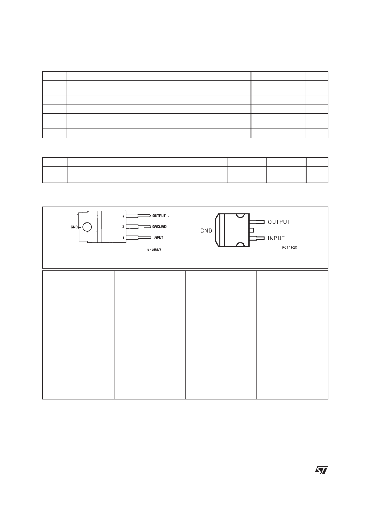
CONNECTION DIAGRAM AND ORDERING NUMBERS(top view)
TO-220 D2PAK
THERMALDATA
Symbol Parameter D2PAK TO-220 Unit
R
thj-cas e
R
thj-amb
Thermal Resistance Junction-case Max
Thermal Resistance Junction-ambient Max
3
62.5
3
50
o
C/W
o
C/W
Type TO-220 D
2
PAK (*) Output Voltage
L7805AB
L7805AC
L7806AB
L7806AC
L7808AB
L7808AC
L7809AB
L7809AC
L7812AB
L7812AC
L7815AB
L7815AC
L7818AB
L7818AC
L7820AB
L7820AC
L7824AB
L7824AC
L7805ABV
L7805ACV
L7806ABV
L7806ACV
L7808ABV
L7808ACV
L7809ABV
L7809ACV
L7812ABV
L7812ACV
L7815ABV
L7815ACV
L7818ABV
L7818ACV
L7820ABV
L7820ACV
L7824ABV
L7824ACV
L7805ABD2T
L7805ACD2T
L7806ABD2T
L7806ACD2T
L7808ABD2T
L7808ACD2T
L7809ABD2T
L7809ACD2T
L7812ABD2T
L7812ACD2T
L7815ABD2T
L7815ACD2T
5V
5V
6V
6V
8V
8V
9V
9V
12V
12V
15V
15V
18V
18V
24V
24V
(*) AVAILABLE IN TAPE AND REEL WITH ”-TR” SUFFIX
ABSOLUTE MAXIMUM RATINGS
Symbol Parameter Value Unit
V
i
DC InputVoltage (for VO= 5 to 18V)
(forV
O
= 20,24V)
35
40
V
V
I
o
OutputCurrent Internally limited
P
tot
PowerDissipation Internally limited
T
op
OperatingJunction TemperatureRange (for L7800AC)
(for L7800AB)
0to150
-40 to 125
o
C
o
C
T
stg
StorageTemperature Range - 65 to 150
o
C
L7800AB/AC
2/17
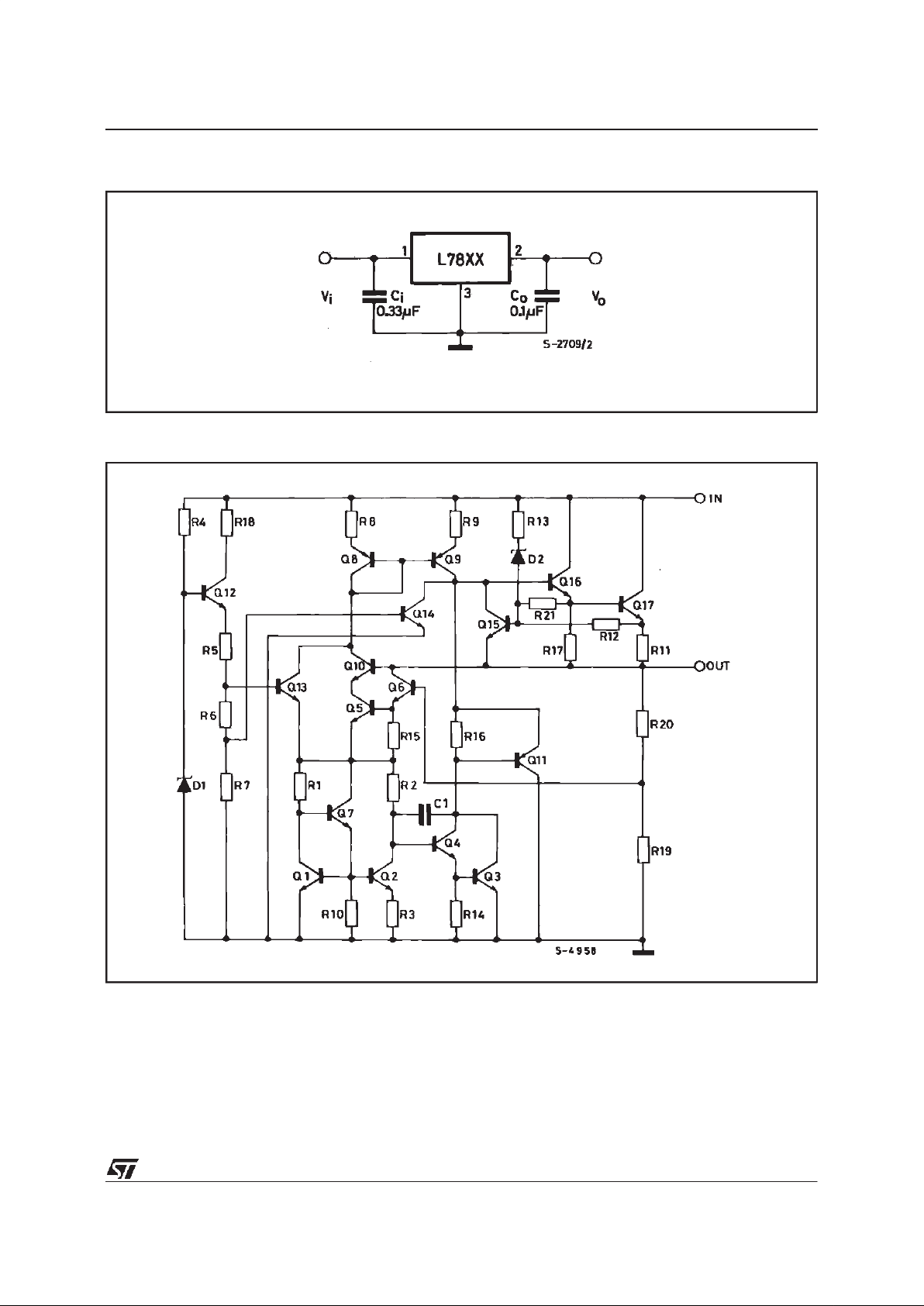
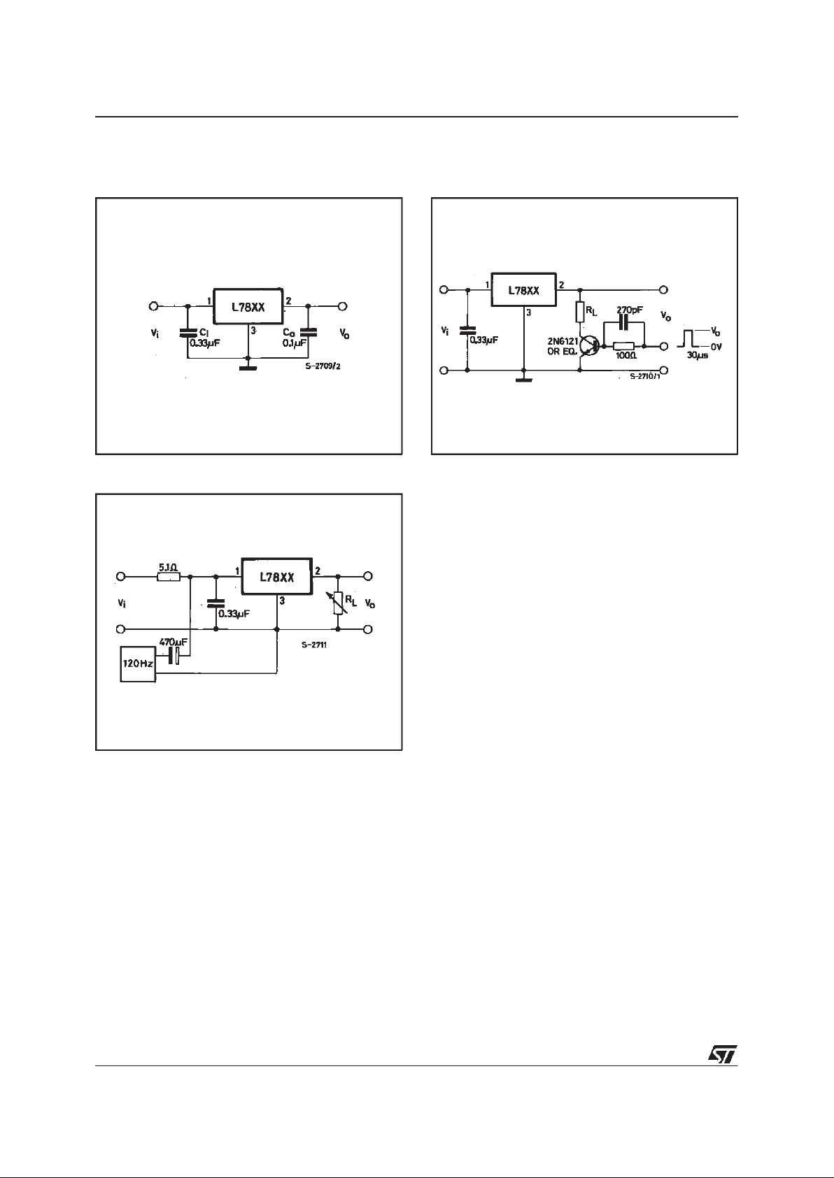
APPLICATION CIRCUIT
SCHEMATIC DIAGRAM
L7800AB/AC
3/17
TESTCIRCUITS
Figure3 : RippleRejection.
Figure2 : Load Regulation.Figure1 : DC Parameter
L7800AB/AC
4/17
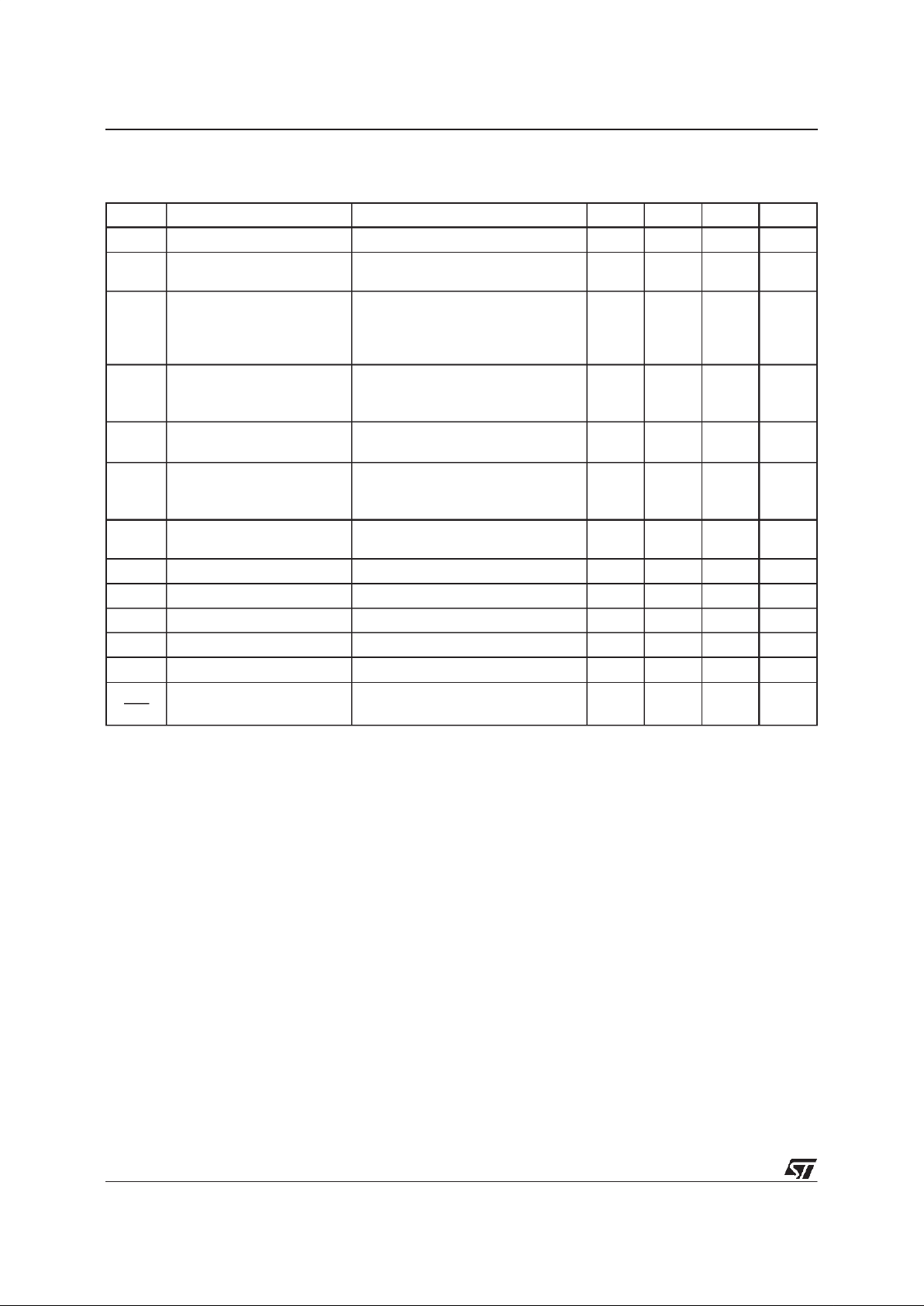
* Load and line regulation are specified at constant junction temperature. Changes in Vodue to heating effects must be taken into account
separately. Pulse testing with low duty cycle is used.
ELECTRICAL CHARACTERISTICS FOR L7805A
(V
i
= 10V,Io= 1A, Tj= 0 to125oC (L7805AC),
T
j
= -40to 125oC (L7805AB)unless otherwise specified)
Symbol Parameter Test Conditions Min. Typ. Max. Unit
V
o
OutputVoltage Tj=25oC 4.955.1V
V
o
OutputVoltage Io=5 mA to 1 A Po≤ 15W
V
i
= 7.5 to 20 V
4.855.2V
∆V
o
* LineRegulation Vi= 7.5 to 25 V Io=500mA
V
i
= 8 to12 V
V
i
= 8 to12 V Tj=25oC
V
i
= 7.3 to 20 V Tj=25oC
7
10
2
7
50
5
25
50
mV
mV
mV
mV
∆V
o
* Load Regulation Io=5 mA to 1 A
I
o
=5 mA to 1.5A Tj=25oC
I
o
=250 to 750 mA
25
30
8
100
100
50
mV
mV
mV
I
d
QuiescentCurrent Tj=25oC4.36
6
mA
∆
I
d
QuiescentCurrent Change Vi= 8 to25 V Io= 500 mA
V
i
= 7.5 to 20 V Tj=25oC
I
o
=5 mA to 1 A
0.8
0.8
0.5
mA
mA
mA
SVR Supply VoltageRejection V
i
= 8 to18 V f= 120Hz
I
o
=500 mA
68 dB
V
d
Dropout Voltage Io=1A Tj=25oC2V
e
N
OutputNoise Voltage B = 10Hzto 100KHz Tj=25oC10µV/V
o
R
o
OutputResistance f = 1KHz 17 mΩ
I
sc
ShortCircuitCurrent Vi=35V T
amb
=25oC0.2A
I
scp
ShortCircuitPeack Current Tj=25oC2.2A
∆
V
o
∆
T
OutputVoltageDrift -1.1 mV/oC
L7800AB/AC
5/17
ELECTRICAL CHARACTERISTICS FOR L7806A
(V
i
= 11V,Io= 1A, Tj= 0 to125oC (L7806AC),
T
j
= -40to 125oC (L7806AB)unless otherwise specified)
Symbol Parameter Test Conditions Min. Typ. Max. Unit
V
o
OutputVoltage Tj=25oC5.8866.12V
V
o
OutputVoltage Io=5 mA to 1 A P
o
≤
15 W
V
i
= 8.6 to 21 V
5.76 6 6.24 V
∆
V
o
* LineRegulation Vi= 8.6 to 25 V Io=500mA
V
i
= 9 to13 V
V
i
= 9 to13 V Tj=25oC
V
i
= 8.3 to 21 V Tj=25oC
9
11
3
9
60
60
30
60
mV
mV
mV
mV
∆V
o
* Load Regulation Io=5 mA to 1 A
I
o
=5 mA to 1.5A Tj=25oC
I
o
=250 to 750 mA
25
30
10
100
100
50
mV
mV
mV
I
d
QuiescentCurrent Tj=25oC4.36
6
mA
∆
I
d
QuiescentCurrent Change Vi= 9 to25 V Io= 500 mA
V
i
= 8.6 to 21 V Tj=25oC
I
o
=5 mA to 1 A
0.8
0.8
0.5
mA
mA
mA
SVR Supply VoltageRejection V
i
= 9 to19 V f= 120Hz
I
o
=500 mA
65 dB
V
d
Dropout Voltage Io=1A Tj=25oC2V
e
N
OutputNoise Voltage B = 10Hzto 100KHz Tj=25oC10
µ
V/V
o
R
o
OutputResistance f = 1KHz 17 m
Ω
I
sc
ShortCircuitCurrent Vi=35V T
amb
=25oC0.2A
I
scp
ShortCircuitPeack Current Tj=25oC2.2A
∆
V
o
∆
T
OutputVoltageDrift -0.8 mV/oC
* Load and line regulation are specified at constant junction temperature. Changes in Vodue to heating effects must be taken into account
separately. Pulse testing with low duty cycle is used.
L7800AB/AC
6/17
 Loading...