

L7800
SERIES
POSITIVE VOLTAGE REGULATORS
November 1999
■ OUTPUT CURRENT UPTO1.5 A
■ OUTPUT VOLTAGESOF 5;5.2; 6;8; 8.5; 9;
12;15; 18; 24V
■ THERMAL OVERLOADPROTECTION
■ SHORTCIRCUIT PROTECTION
■ OUTPUT TRANSITIONSOAPROTECTION
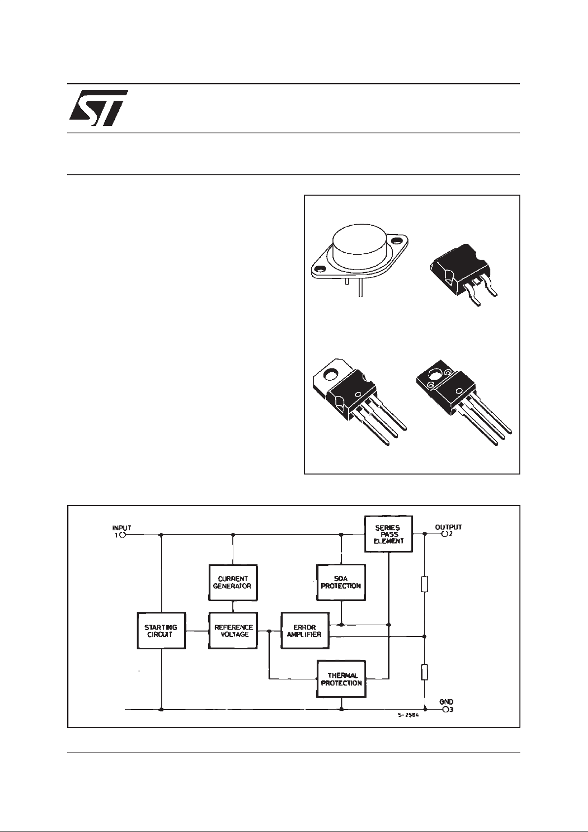
DESCRIPTION
The L7800 series of three-terminal positive
regulators is available in TO-220 ISOWATT220
TO-3 and D
2
PAK packages and several fixed
output voltages, making it useful in a wide range
of applications.Theseregulators can provide local
on-card regulation, eliminating the distribution
problems associated with single point regulation.
Each type employs internal current limiting,
thermal shut-down and safe area protection,
making it essentially indestructible. If adequate
heat sinking is provided,they can deliver over 1A
output current. Although designed primarily as
fixed voltage regulators, these devices can be
used with external components to obtain
adjustablevoltages and currents.
1
2
TO-3
TO-220 ISOWATT220
D2PAK
BLOCKDIAGRAM
1/25

CONNECTION DIAGRAM AND ORDERING NUMBERS(top view)
TO-220 & ISOWATT220 TO-3D2PAK
THERMALDATA
Symbol Parameter D2PAK TO-220 ISOWATT220 TO-3 Unit
R
thj-cas e
R
thj-amb
Thermal Resistance Junction-case Max
Thermal Resistance Junction-ambient Max
3
62.5
3
50
4
60
4
35
o
C/W
o
C/W
Type TO-220 D
2
PAK (*) ISOWATT220 TO-3 Output Voltage
L7805
L7805C
L7852C
L7806
L7806C
L7808
L7808C
L7885C
L7809C
L7812
L7812C
L7815
L7815C
L7818
L7818C
L7820
L7820C
L7824
L7824C
L7805CV
L7852CV
L7806CV
L7808CV
L7885CV
L7809CV
L7812CV
L7815CV
L7818CV
L7820CV
L7824CV
L7805CD2T
L7852CD2T
L7806CD2T
L7808CD2T
L7885CD2T
L7809CD2T
L7812CD2T
L7815CD2T
L7818CD2T
L7820CD2T
L7824CD2T
L7805CP
L7852CP
L7806CP
L7808CP
L7885CP
L7809CP
L7812CP
L7815CP
L7818CP
L7820CP
L7824CP
L7805T
L7805CT
L7852CT
L7806T
L7806CT
L7808T
L7808CT
L7885CT
L7809CT
L7812T
L7812CT
L7815T
L7815CT
L7818T
L7818CT
L7820T
L7820CT
L7824T
L7824CT
5V
5V
5.2V
6V
6V
8V
8V
8.5V
9V
12V
12V
15V
15V
18V
18V
20V
20V
24V
24V
(*) AVAILABLE IN TAPE AND REEL WITH ”-TR” SUFFIX
ABSOLUTE MAXIMUM RATINGS
Symbol Parameter Value Unit
V
i
DC InputVoltage(forVO= 5 to 18V)
(forV
O
= 20,24V)
35
40
V
V
I
o
OutputCurrent Internally limited
P
tot
PowerDissipation Internally limited
T
op
OperatingJunctionTemperatureRange (for L7800)
(for L7800C)
-55 to 150
0to150
o
C
o
C
T
stg
StorageTemperature Range -65 to 150
o
C
L7800
2/25
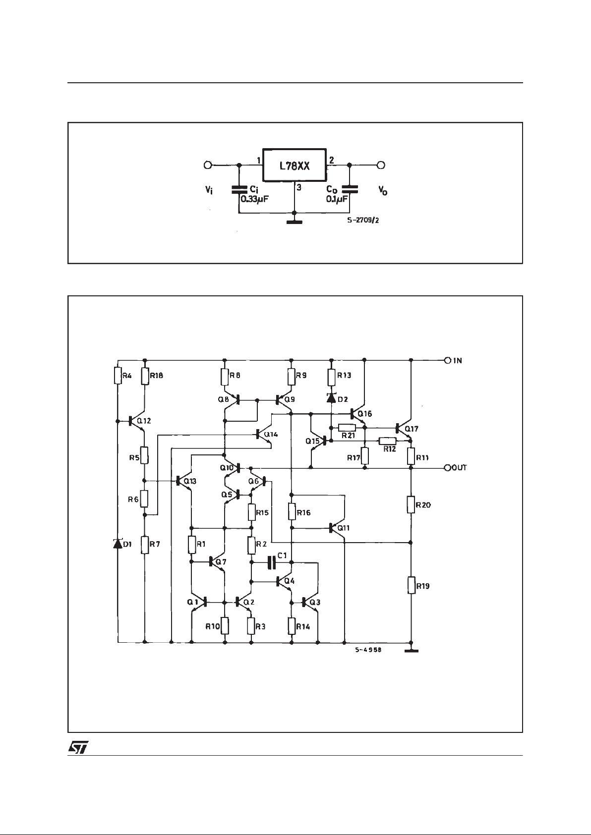
APPLICATION CIRCUIT
SCHEMATIC DIAGRAM
L7800
3/25
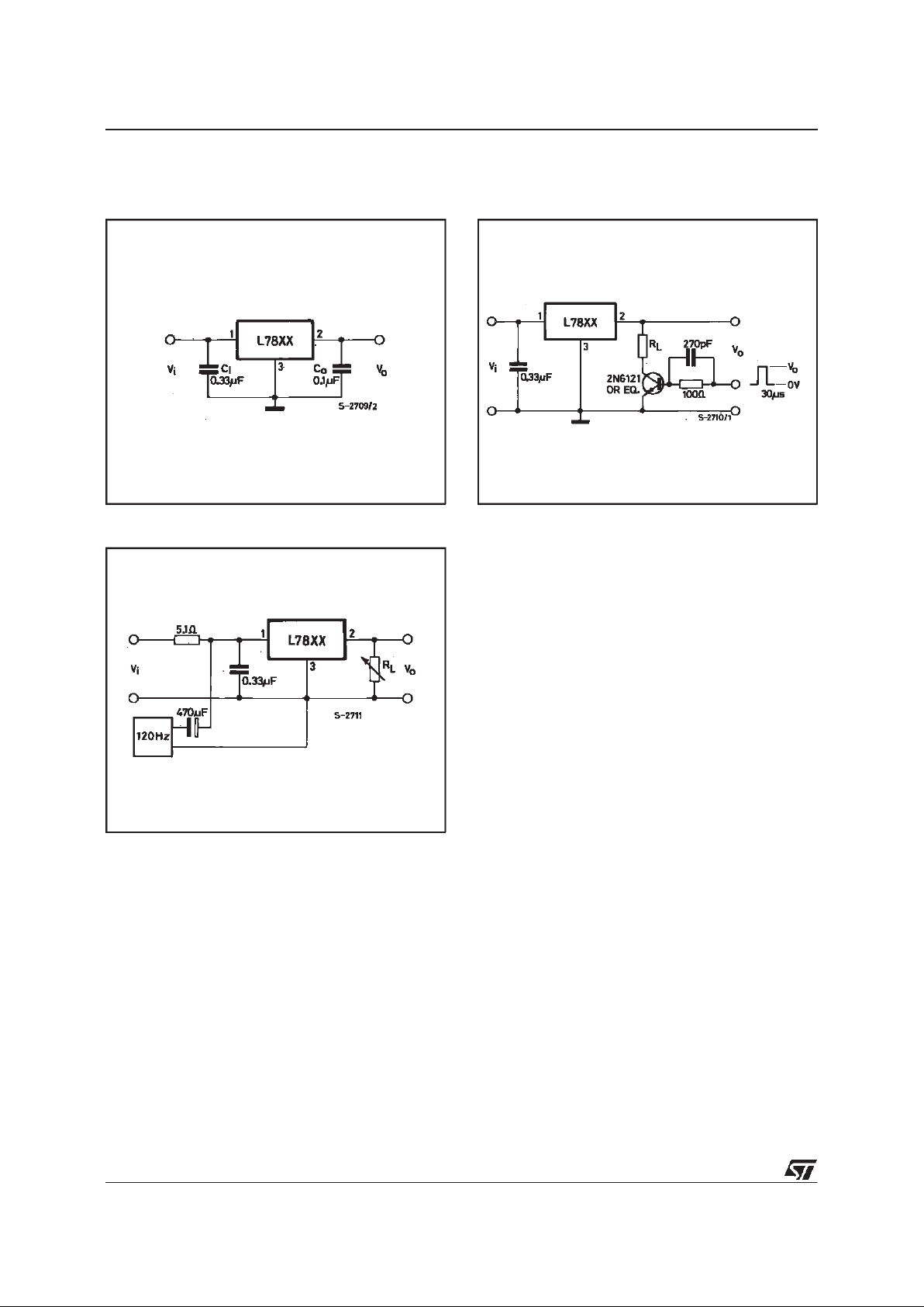
TESTCIRCUITS
Figure3 : RippleRejection.
Figure2 : Load Regulation.Figure1 : DC Parameter
L7800
4/25
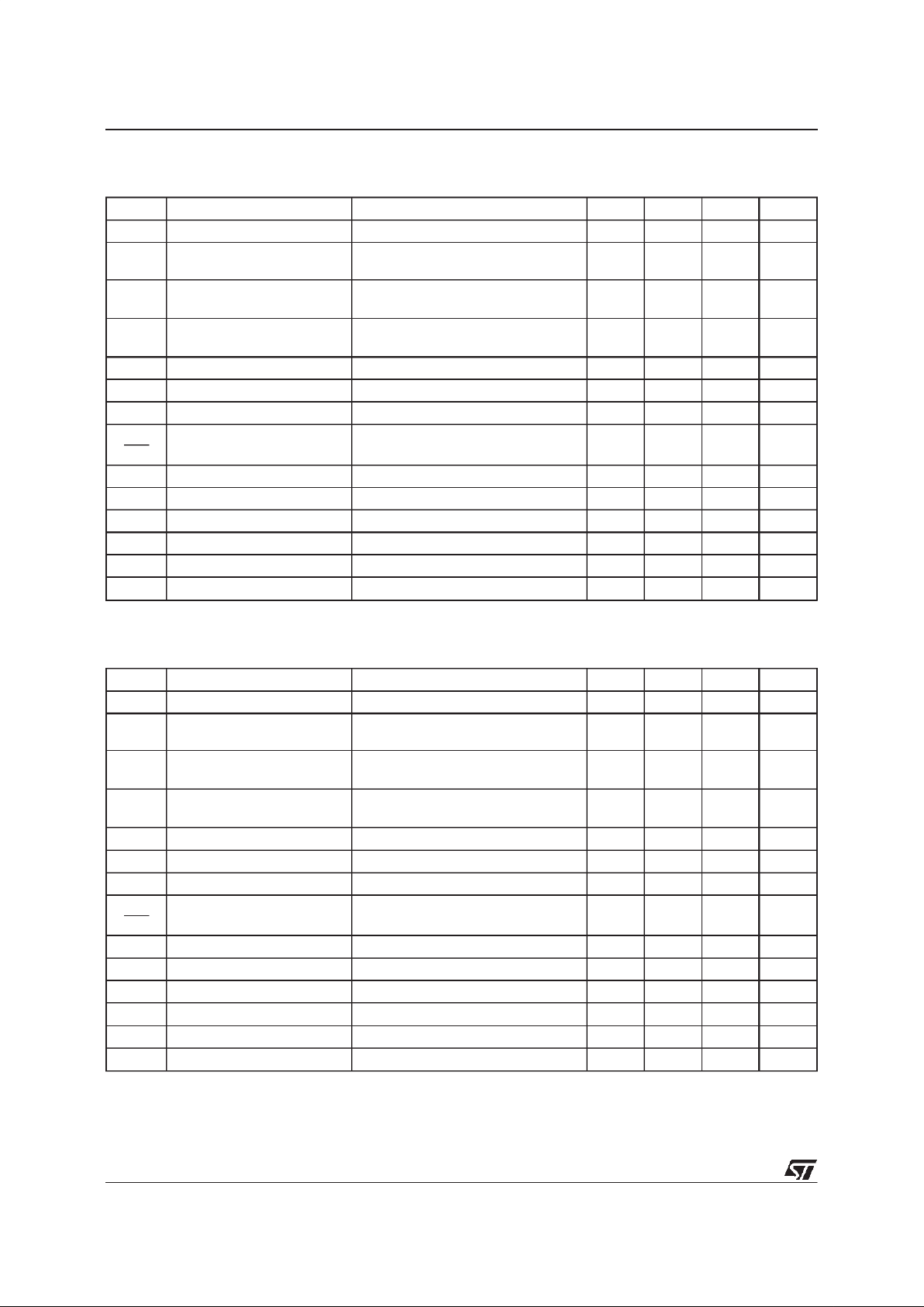
ELECTRICALCHARACTERISTICS FOR L7806
(refer to the test circuits, T
j
= -55 to 150oC,
V
i
= 15V, Io=500 mA, Ci=0.33 µF, Co=0.1 µF unlessotherwisespecified)
Symbol Parameter Test Conditions Min. Typ. Max. Unit
V
o
OutputVoltage Tj=25oC5.7566.25V
V
o
OutputVoltage Io=5 mA to 1 A Po≤ 15W
V
i
= 9 to 21 V
5.65 6 6.35 V
∆
V
o
* LineRegulation Vi= 8 to 25 V Tj=25oC
V
i
= 9 to 13 V Tj=25oC
60
30
mV
mV
∆V
o
* LoadRegulation Io=5 to 1500 mA Tj=25oC
I
o
=250 to 750mA Tj=25oC
100
30
mV
mV
I
d
QuiescentCurrent Tj=25oC6mA
∆
I
d
QuiescentCurrentChange Io=5 to 1000 mA 0.5 mA
∆
I
d
QuiescentCurrentChange Vi= 9 to 25 V 0.8 mA
∆
V
o
∆
T
OutputVoltageDrift Io=5mA 0.7 mV/oC
eN OutputNoiseVoltage B = 10Hz to 100KHz T
j
=25oC40µV/V
O
SVR Supply Voltage Rejection Vi= 9 to 19 V f = 120Hz 65 dB
V
d
Dropout Voltage Io=1A Tj=25oC22.5V
R
o
OutputResistance f = 1 KHz 19 m
Ω
I
sc
ShortCircuitCurrent Vi=35V Tj=25oC0.751.2A
I
scp
ShortCircuitPeak Current Tj=25oC 1.3 2.2 3.3 A
ELECTRICALCHARACTERISTICS FOR L7805 (refer to the test circuits, Tj= -55 to 150oC,
V
i
= 10V, Io=500 mA, Ci=0.33 µF, Co=0.1 µF unlessotherwisespecified)
Symbol Parameter Test Conditions Min. Typ. Max. Unit
V
o
OutputVoltage Tj=25oC 4.855.2V
V
o
OutputVoltage Io=5 mA to 1 A P
o
≤
15W
V
i
= 8 to 20 V
4.65 5 5.35 V
∆
V
o
* LineRegulation Vi= 7 to 25 V Tj=25oC
V
i
= 8 to 12 V Tj=25oC
3
1
50
25
mV
mV
∆
V
o
* LoadRegulation Io=5 to 1500 mA Tj=25oC
I
o
=250 to 750mA Tj=25oC
100
25
mV
mV
I
d
QuiescentCurrent Tj=25oC6mA
∆I
d
QuiescentCurrentChange Io=5 to 1000 mA 0.5 mA
∆
I
d
QuiescentCurrentChange Vi= 8 to 25 V 0.8 mA
∆
V
o
∆
T
OutputVoltageDrift Io=5mA 0.6 mV/oC
eN OutputNoiseVoltage B = 10Hz to 100KHz T
j
=25oC40
µ
V/V
O
SVR Supply Voltage Rejection Vi= 8 to 18 V f = 120Hz 68 dB
V
d
Dropout Voltage Io=1A Tj=25oC22.5V
R
o
OutputResistance f = 1 KHz 17 mΩ
I
sc
ShortCircuitCurrent Vi=35V Tj=25oC0.751.2A
I
scp
ShortCircuitPeak Current Tj=25oC 1.3 2.2 3.3 A
* Load and line regulation are specified at constant junction temperature. Changes in Vodue to heating effects must be taken into account
separately. Pulce testing with low duty cycle is used.
L7800
5/25

ELECTRICALCHARACTERISTICS FOR L7812
(refer to the test circuits, T
j
= -55 to 150oC,
V
i
= 19V, Io=500 mA, Ci=0.33 µF, Co=0.1 µF unlessotherwisespecified)
Symbol Parameter Test Conditions Min. Typ. Max. Unit
V
o
OutputVoltage Tj=25oC 11.5 12 1 2.5 V
V
o
OutputVoltage Io=5 mA to 1 A Po≤ 15W
V
i
= 15.5to 27 V
11.4 12 12.6 V
∆
V
o
* LineRegulation Vi= 14.5to 30 V Tj=25oC
V
i
=16to22V Tj=25oC
120
60
mV
mV
∆V
o
* LoadRegulation Io=5 to 1500 mA Tj=25oC
I
o
=250 to 750mA Tj=25oC
100
60
mV
mV
I
d
QuiescentCurrent Tj=25oC6mA
∆
I
d
QuiescentCurrentChange Io=5 to 1000 mA 0.5 mA
∆
I
d
QuiescentCurrentChange Vi=15to30V 0.8 mA
∆
V
o
∆
T
OutputVoltageDrift Io=5mA 1.5 mV/oC
eN OutputNoiseVoltage B = 10Hzto 100KHz T
j
=25oC40µV/V
O
SVR Supply VoltageRejection Vi= 15 to 25 V f= 120 Hz 61 dB
V
d
Dropout Voltage Io=1A Tj=25oC22.5V
R
o
OutputResistance f = 1KHz 18 m
Ω
I
sc
ShortCircuitCurrent Vi=35V Tj=25oC0.751.2A
I
scp
ShortCircuitPeak Current Tj=25oC 1.3 2.2 3.3 A
ELECTRICALCHARACTERISTICS FOR L7808 (refer to the test circuits, Tj= -55 to 150oC,
V
i
= 14V, Io=500 mA, Ci=0.33 µF, Co=0.1 µF unlessotherwisespecified)
Symbol Parameter Test Conditions Min. Typ. Max. Unit
V
o
OutputVoltage Tj=25oC 7.788.3V
V
o
OutputVoltage Io=5 mA to 1 A P
o
≤
15W
V
i
= 11.5to 23 V
7.688.4V
∆
V
o
* LineRegulation Vi= 10.5to 25 V Tj=25oC
V
i
=11to17V Tj=25oC
80
40
mV
mV
∆
V
o
* LoadRegulation Io=5 to 1500 mA Tj=25oC
I
o
=250 to 750mA Tj=25oC
100
40
mV
mV
I
d
Quiescent Current Tj=25oC6mA
∆I
d
Quiescent CurrentChange Io=5 to 1000 mA 0.5 mA
∆
I
d
Quiescent CurrentChange Vi= 11.5to 25 V 0.8 mA
∆
V
o
∆
T
OutputVoltageDrift Io=5mA 1 mV/oC
eN OutputNoiseVoltage B = 10Hzto 100KHz T
j
=25oC40
µ
V/V
O
SVR Supply VoltageRejection Vi= 11.5to 21.5 V f =120 Hz 62 dB
V
d
Dropout Voltage Io=1A Tj=25oC22.5V
R
o
OutputResistance f = 1KHz 16 mΩ
I
sc
ShortCircuitCurrent Vi=35V Tj=25oC0.751.2A
I
scp
ShortCircuitPeak Current Tj=25oC 1.3 2.2 3.3 A
* Load and line regulation are specified at constant junction temperature. Changes in Vodue to heating effects must be taken into account
separately. Pulce testing with low duty cycle is used.
L7800
6/25

ELECTRICALCHARACTERISTICS FOR L7818
(refer to the test circuits, T
j
= -55 to 150oC,
V
i
= 26V, Io=500 mA, Ci=0.33 µF, Co=0.1 µF unlessotherwisespecified)
Symbol Parameter Test Conditions Min. Typ. Max. Unit
V
o
OutputVoltage Tj=25oC 17.3 18 1 8.7 V
V
o
OutputVoltage Io=5 mA to 1 A Po≤ 15W
V
i
=22to33V
17.1 18 18.9 V
∆
V
o
* LineRegulation Vi=21to33V Tj=25oC
V
i
=24to30V Tj=25oC
180
90
mV
mV
∆V
o
* LoadRegulation Io=5 to 1500 mA Tj=25oC
I
o
=250 to 750mA Tj=25oC
180
90
mV
mV
I
d
Quiescent Current Tj=25oC6mA
∆
I
d
Quiescent CurrentChange Io=5 to 1000 mA 0.5 mA
∆
I
d
Quiescent CurrentChange Vi=22to33V 0.8 mA
∆
V
o
∆
T
OutputVoltageDrift Io=5mA 2.3 mV/oC
eN OutputNoiseVoltage B = 10Hzto 100KHz T
j
=25oC40µV/V
O
SVR Supply VoltageRejection Vi= 22 to 32 V f= 120 Hz 59 dB
V
d
Dropout Voltage Io=1A Tj=25oC22.5V
R
o
OutputResistance f = 1KHz 22 m
Ω
I
sc
ShortCircuitCurrent Vi=35V Tj=25oC0.751.2A
I
scp
ShortCircuitPeak Current Tj=25oC 1.3 2.2 3.3 A
ELECTRICALCHARACTERISTICS FOR L7815 (refer to the test circuits, Tj= -55 to 150oC,
V
i
= 23V, Io=500 mA, Ci=0.33 µF, Co=0.1 µF unlessotherwisespecified)
Symbol Parameter Test Conditions Min. Typ. Max. Unit
V
o
OutputVoltage Tj=25oC 14.4 15 1 5.6 V
V
o
OutputVoltage Io=5 mA to 1 A P
o
≤
15W
V
i
= 18.5to 30 V
14.25 15 15.75 V
∆
V
o
* LineRegulation Vi= 17.5to 30 V Tj=25oC
V
i
=20to26V Tj=25oC
150
75
mV
mV
∆
V
o
* LoadRegulation Io=5 to 1500 mA Tj=25oC
I
o
=250 to 750mA Tj=25oC
150
75
mV
mV
I
d
Quiescent Current Tj=25oC6mA
∆I
d
Quiescent CurrentChange Io=5 to 1000 mA 0.5 mA
∆
I
d
Quiescent CurrentChange Vi= 18.5to 30 V 0.8 mA
∆
V
o
∆
T
OutputVoltageDrift Io=5mA 1.8 mV/oC
eN OutputNoiseVoltage B = 10Hzto 100KHz T
j
=25oC40
µ
V/V
O
SVR Supply VoltageRejection Vi= 18.5to 28.5 V f =120 Hz 60 dB
V
d
Dropout Voltage Io=1A Tj=25oC22.5V
R
o
OutputResistance f = 1KHz 19 mΩ
I
sc
ShortCircuitCurrent Vi=35V Tj=25oC0.751.2A
I
scp
ShortCircuitPeak Current Tj=25oC 1.3 2.2 3.3 A
* Load and line regulation are specified at constant junction temperature. Changes in Vodue to heating effects must be taken into account
separately. Pulce testing with low duty cycle is used.
L7800
7/25
ELECTRICALCHARACTERISTICS FOR L7824
(refer to the test circuits, T
j
= -55 to 150oC,
V
i
= 33V, Io=500 mA, Ci=0.33 µF, Co=0.1 µF unlessotherwisespecified)
Symbol Parameter Test Conditions Min. Typ. Max. Unit
V
o
OutputVoltage Tj=25oC 232425V
V
o
OutputVoltage Io=5 mA to 1 A Po≤ 15W
V
i
=28to38V
22.8 24 25.2 V
∆
V
o
* LineRegulation Vi=27to38V Tj=25oC
V
i
=30to36V Tj=25oC
240
120
mV
mV
∆V
o
* LoadRegulation Io=5 to 1500 mA Tj=25oC
I
o
=250 to 750mA Tj=25oC
240
120
mV
mV
I
d
Quiescent Current Tj=25oC6mA
∆
I
d
Quiescent CurrentChange Io=5 to 1000 mA 0.5 mA
∆
I
d
Quiescent CurrentChange Vi=28to38V 0.8 mA
∆
V
o
∆
T
OutputVoltageDrift Io=5mA 3 mV/oC
eN OutputNoiseVoltage B = 10Hzto 100KHz T
j
=25oC40µV/V
O
SVR Supply VoltageRejection Vi= 28 to 38 V f= 120 Hz 56 dB
V
d
Dropout Voltage Io=1A Tj=25oC22.5V
R
o
OutputResistance f = 1KHz 28 m
Ω
I
sc
ShortCircuitCurrent Vi=35V Tj=25oC0.751.2A
I
scp
ShortCircuitPeak Current Tj=25oC 1.3 2.2 3.3 A
ELECTRICALCHARACTERISTICS FOR L7820 (refer to the test circuits, Tj= -55 to 150oC,
V
i
= 28V, Io=500 mA, Ci=0.33 µF, Co=0.1 µF unlessotherwisespecified)
Symbol Parameter Test Conditions Min. Typ. Max. Unit
V
o
OutputVoltage Tj=25oC 19.2 20 2 0.8 V
V
o
OutputVoltage Io=5 mA to 1 A P
o
≤
15W
V
i
=24to35V
19 20 21 V
∆
V
o
* LineRegulation Vi= 22.5to 35 V Tj=25oC
V
i
=26to32V Tj=25oC
200
100
mV
mV
∆
V
o
* LoadRegulation Io=5 to 1500 mA Tj=25oC
I
o
=250 to 750mA Tj=25oC
200
100
mV
mV
I
d
Quiescent Current Tj=25oC6mA
∆I
d
Quiescent CurrentChange Io=5 to 1000 mA 0.5 mA
∆
I
d
Quiescent CurrentChange Vi=24to35V 0.8 mA
∆
V
o
∆
T
OutputVoltageDrift Io=5mA 2.5 mV/oC
eN OutputNoiseVoltage B = 10Hzto 100KHz T
j
=25oC40
µ
V/V
O
SVR Supply VoltageRejection Vi= 24 to 35 V f= 120 Hz 58 dB
V
d
Dropout Voltage Io=1A Tj=25oC22.5V
R
o
OutputResistance f = 1KHz 24 mΩ
I
sc
ShortCircuitCurrent Vi=35V Tj=25oC0.751.2A
I
scp
ShortCircuitPeak Current Tj=25oC 1.3 2.2 3.3 A
* Load and line regulation are specified at constant junction temperature. Changes in Vodue to heating effects must be taken into account
separately. Pulce testing with low duty cycle is used.
L7800
8/25
 Loading...