

SGS Thomson Microelectronics L7824ABV, L7820ACV, L7824ACV, L7820ABV, L7818ACV Datasheet
...
L7800AB/AC
SERIES
PRECISION 1A REGULATORS
November 1999
■ OUTPUT CURRENT INEXCESSOF1 A
■
OUTPUT VOLTAGESOF 5;6; 8; 9; 12; 15; 18;
20;24V
■
THERMAL OVERLOADPROTECTION
■ OUTPUT TRANSITIONSOAPROTECTION
■ 2%OUTPUTVOLTAGETOLERANCE
■
GUARANTEEDINEXTENDED
TEMPERATURERANGE
DESCRIPTION
The L7800A series of three-terminal positive
regulators is available in TO-220 and D
2
PAK
packages and several fixed output voltages,
making it useful in a wide range of
applications.These regulators can provide local
on-card regulation, eliminating the distribution
problems associated with single point regulation.
Each type employs internal current limiting,
thermal shut-down and safe area protection,
making it essentially indestructible. If adequate
heat sinking is provided, they can deliver over 1A
output current. Although designed primarily as
fixed voltage regulators, these devices can be
used with external components to obtain
adjustablevoltages and currents.
TO-220
D
2
PAK
BLOCKDIAGRAM
1/17
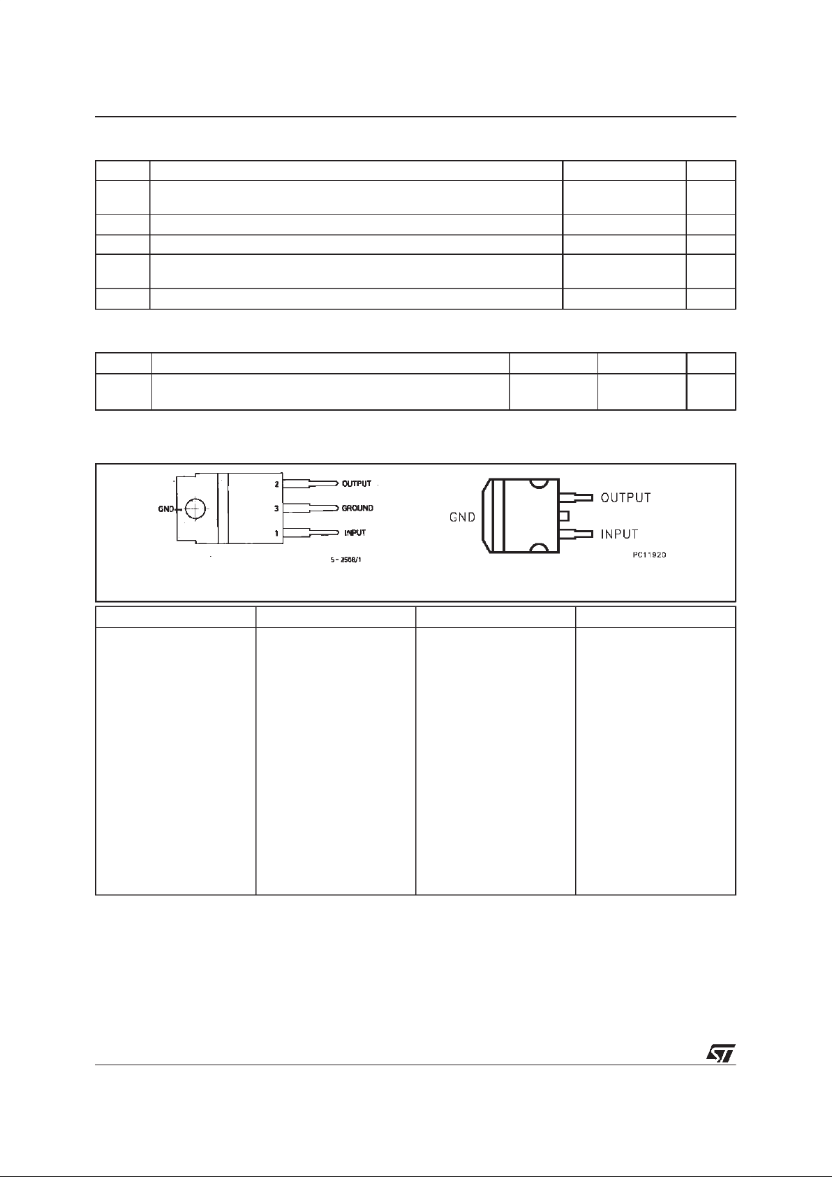
CONNECTION DIAGRAM AND ORDERING NUMBERS(top view)
TO-220 D2PAK
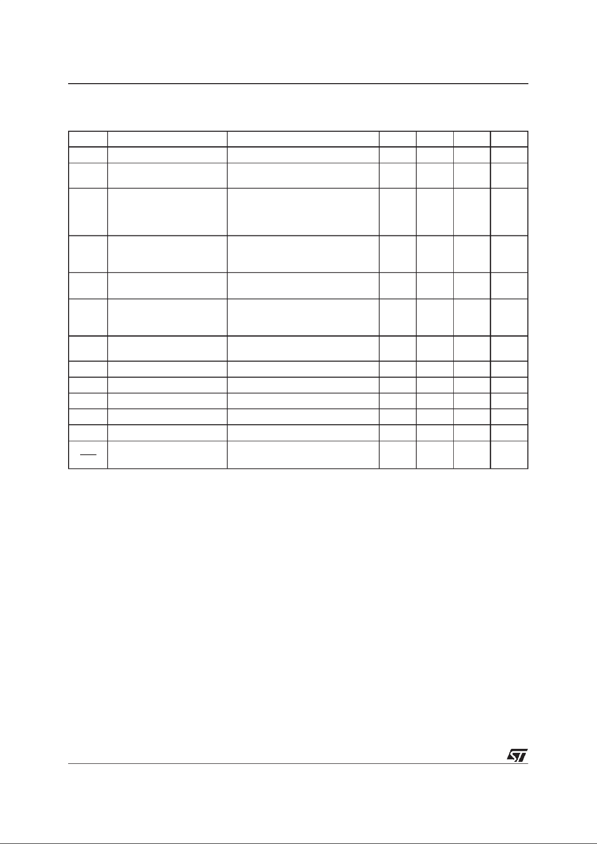
THERMALDATA
Symbol Parameter D2PAK TO-220 Unit
R
thj-cas e
R
thj-amb
Thermal Resistance Junction-case Max
Thermal Resistance Junction-ambient Max
3
62.5
3
50
o
C/W
o
C/W
Type TO-220 D
2
PAK (*) Output Voltage
L7805AB
L7805AC
L7806AB
L7806AC
L7808AB
L7808AC
L7809AB
L7809AC
L7812AB
L7812AC
L7815AB
L7815AC
L7818AB
L7818AC
L7820AB
L7820AC
L7824AB
L7824AC
L7805ABV
L7805ACV
L7806ABV
L7806ACV
L7808ABV
L7808ACV
L7809ABV
L7809ACV
L7812ABV
L7812ACV
L7815ABV
L7815ACV
L7818ABV
L7818ACV
L7820ABV
L7820ACV
L7824ABV
L7824ACV
L7805ABD2T
L7805ACD2T
L7806ABD2T
L7806ACD2T
L7808ABD2T
L7808ACD2T
L7809ABD2T
L7809ACD2T
L7812ABD2T
L7812ACD2T
L7815ABD2T
L7815ACD2T
5V
5V
6V
6V
8V
8V
9V
9V
12V
12V
15V
15V
18V
18V
24V
24V
(*) AVAILABLE IN TAPE AND REEL WITH ”-TR” SUFFIX
ABSOLUTE MAXIMUM RATINGS
Symbol Parameter Value Unit
V
i
DC InputVoltage (for VO= 5 to 18V)
(forV
O
= 20,24V)
35
40
V
V
I
o
OutputCurrent Internally limited
P
tot
PowerDissipation Internally limited
T
op
OperatingJunction TemperatureRange (for L7800AC)
(for L7800AB)
0to150
-40 to 125
o
C
o
C
T
stg
StorageTemperature Range - 65 to 150
o
C
L7800AB/AC
2/17
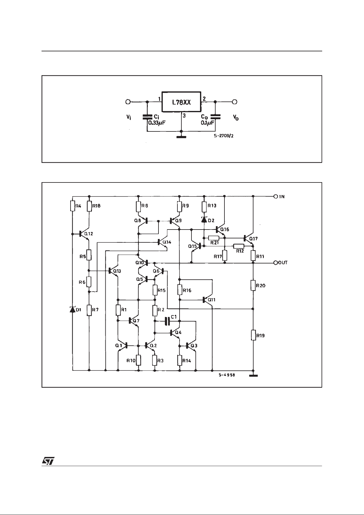
APPLICATION CIRCUIT
SCHEMATIC DIAGRAM
L7800AB/AC
3/17
TESTCIRCUITS
Figure3 : RippleRejection.
Figure2 : Load Regulation.Figure1 : DC Parameter
L7800AB/AC
4/17
* Load and line regulation are specified at constant junction temperature. Changes in Vodue to heating effects must be taken into account
separately. Pulse testing with low duty cycle is used.
ELECTRICAL CHARACTERISTICS FOR L7805A
(V
i
= 10V,Io= 1A, Tj= 0 to125oC (L7805AC),
T
j
= -40to 125oC (L7805AB)unless otherwise specified)
Symbol Parameter Test Conditions Min. Typ. Max. Unit
V
o
OutputVoltage Tj=25oC 4.955.1V
V
o
OutputVoltage Io=5 mA to 1 A Po≤ 15W
V
i
= 7.5 to 20 V
4.855.2V
∆V
o
* LineRegulation Vi= 7.5 to 25 V Io=500mA
V
i
= 8 to12 V
V
i
= 8 to12 V Tj=25oC
V
i
= 7.3 to 20 V Tj=25oC
7
10
2
7
50
5
25
50
mV
mV
mV
mV
∆V
o
* Load Regulation Io=5 mA to 1 A
I
o
=5 mA to 1.5A Tj=25oC
I
o
=250 to 750 mA
25
30
8
100
100
50
mV
mV
mV
I
d
QuiescentCurrent Tj=25oC4.36
6
mA
∆
I
d
QuiescentCurrent Change Vi= 8 to25 V Io= 500 mA
V
i
= 7.5 to 20 V Tj=25oC
I
o
=5 mA to 1 A
0.8
0.8
0.5
mA
mA
mA
SVR Supply VoltageRejection V
i
= 8 to18 V f= 120Hz
I
o
=500 mA
68 dB
V
d
Dropout Voltage Io=1A Tj=25oC2V
e
N
OutputNoise Voltage B = 10Hzto 100KHz Tj=25oC10µV/V
o
R
o
OutputResistance f = 1KHz 17 mΩ
I
sc
ShortCircuitCurrent Vi=35V T
amb
=25oC0.2A
I
scp
ShortCircuitPeack Current Tj=25oC2.2A
∆
V
o
∆
T
OutputVoltageDrift -1.1 mV/oC
L7800AB/AC
5/17
ELECTRICAL CHARACTERISTICS FOR L7806A
(V
i
= 11V,Io= 1A, Tj= 0 to125oC (L7806AC),
T
j
= -40to 125oC (L7806AB)unless otherwise specified)
Symbol Parameter Test Conditions Min. Typ. Max. Unit
V
o
OutputVoltage Tj=25oC5.8866.12V
V
o
OutputVoltage Io=5 mA to 1 A P
o
≤
15 W
V
i
= 8.6 to 21 V
5.76 6 6.24 V
∆
V
o
* LineRegulation Vi= 8.6 to 25 V Io=500mA
V
i
= 9 to13 V
V
i
= 9 to13 V Tj=25oC
V
i
= 8.3 to 21 V Tj=25oC
9
11
3
9
60
60
30
60
mV
mV
mV
mV
∆V
o
* Load Regulation Io=5 mA to 1 A
I
o
=5 mA to 1.5A Tj=25oC
I
o
=250 to 750 mA
25
30
10
100
100
50
mV
mV
mV
I
d
QuiescentCurrent Tj=25oC4.36
6
mA
∆
I
d
QuiescentCurrent Change Vi= 9 to25 V Io= 500 mA
V
i
= 8.6 to 21 V Tj=25oC
I
o
=5 mA to 1 A
0.8
0.8
0.5
mA
mA
mA
SVR Supply VoltageRejection V
i
= 9 to19 V f= 120Hz
I
o
=500 mA
65 dB
V
d
Dropout Voltage Io=1A Tj=25oC2V
e
N
OutputNoise Voltage B = 10Hzto 100KHz Tj=25oC10
µ
V/V
o
R
o
OutputResistance f = 1KHz 17 m
Ω
I
sc
ShortCircuitCurrent Vi=35V T
amb
=25oC0.2A
I
scp
ShortCircuitPeack Current Tj=25oC2.2A
∆
V
o
∆
T
OutputVoltageDrift -0.8 mV/oC
* Load and line regulation are specified at constant junction temperature. Changes in Vodue to heating effects must be taken into account
separately. Pulse testing with low duty cycle is used.
L7800AB/AC
6/17

ELECTRICAL CHARACTERISTICS FOR L7808A
(V
i
= 14V,Io= 1A, Tj= 0 to125oC (L7808AC),
T
j
= -40to 125oC (L7808AB)unless otherwise specified)
Symbol Parameter Test Conditions Min. Typ. Max. Unit
V
o
OutputVoltage Tj=25oC7.8488.16V
V
o
OutputVoltage Io=5 mA to 1 A P
o
≤
15 W
V
i
= 10.6to 23 V
7.788.3V
∆
V
o
* LineRegulation Vi= 10.6to 25 V Io=500 mA
V
i
=11to17V
V
i
=11to17V Tj=25oC
V
i
= 10.4to 23 V Tj=25oC
12
15
5
12
80
80
40
80
mV
mV
mV
mV
∆V
o
* Load Regulation Io=5 mA to 1 A
I
o
=5 mA to 1.5A Tj=25oC
I
o
=250 to 750 mA
25
30
10
100
100
50
mV
mV
mV
I
d
QuiescentCurrent Tj=25oC4.36
6
mA
∆
I
d
QuiescentCurrent Change Vi=11to25V Io=500mA
V
i
= 10.6to 23 V Tj=25oC
I
o
=5 mA to 1 A
0.8
0.8
0.5
mA
mA
mA
SVR Supply VoltageRejection V
i
= 11.5to 21.5 V f =120 Hz
I
o
=500 mA
62 dB
V
d
Dropout Voltage Io=1A Tj=25oC2V
e
N
OutputNoise Voltage B = 10Hzto 100KHz Tj=25oC10
µ
V/V
o
R
o
OutputResistance f = 1KHz 18 m
Ω
I
sc
ShortCircuitCurrent Vi=35V T
amb
=25oC0.2A
I
scp
ShortCircuitPeack Current Tj=25oC2.2A
∆
V
o
∆
T
OutputVoltageDrift -0.8 mV/oC
* Load and line regulation are specified at constant junction temperature. Changes in Vodue to heating effects must be taken into account
separately. Pulse testing with low duty cycle is used.
L7800AB/AC
7/17

ELECTRICAL CHARACTERISTICS FOR L7809A
(V
i
= 15V,Io= 1A, Tj= 0 to125oC (L7809AC),
T
j
= -40to 125oC (L7809AB)unless otherwise specified)
Symbol Parameter Test Conditions Min. Typ. Max. Unit
V
o
OutputVoltage Tj=25oC8.8299.18V
V
o
OutputVoltage Io=5 mA to 1 A P
o
≤
15 W
V
i
= 10.6to 23 V
8.65 9 9.35 V
∆
V
o
* LineRegulation Vi= 10.6to 25 V Io=500 mA
V
i
=11to17V
V
i
=11to17V Tj=25oC
V
i
= 10.4to 23 V Tj=25oC
12
15
5
12
90
90
45
90
mV
mV
mV
mV
∆V
o
* Load Regulation Io=5 mA to 1 A
I
o
=5 mA to 1.5A Tj=25oC
I
o
=250 to 750 mA
25
30
10
100
100
50
mV
mV
mV
I
d
QuiescentCurrent Tj=25oC4.36
6
mA
∆
I
d
QuiescentCurrent Change Vi=11to25V Io=500mA
V
i
= 10.6to 23 V Tj=25oC
I
o
=5 mA to 1 A
0.8
0.8
0.5
mA
mA
mA
SVR Supply VoltageRejection V
i
= 11.5to 21.5 V f =120 Hz
I
o
=500 mA
61 dB
V
d
Dropout Voltage Io=1A Tj=25oC2V
e
N
OutputNoise Voltage B = 10Hzto 100KHz Tj=25oC10
µ
V/V
o
R
o
OutputResistance f = 1KHz 18 m
Ω
I
sc
ShortCircuitCurrent Vi=35V T
amb
=25oC0.2A
I
scp
ShortCircuitPeack Current Tj=25oC2.2A
∆
V
o
∆
T
OutputVoltageDrift -0.8 mV/oC
* Load and line regulation are specified at constant junction temperature. Changes in Vodue to heating effects must be taken into account
separately. Pulse testing with low duty cycle is used.
L7800AB/AC
8/17

ELECTRICAL CHARACTERISTICS FOR L7812A
(V
i
= 19V,Io= 1A, Tj= 0 to125oC (L7812AC),
T
j
= -40to 125oC (L7812AB)unless otherwise specified)
Symbol Parameter Test Conditions Min. Typ. Max. Unit
V
o
OutputVoltage Tj=25oC 11.75 12 12.25 V
V
o
OutputVoltage Io=5 mA to 1 A P
o
≤
15 W
V
i
= 14.8to 27 V
11.5 12 12.5 V
∆
V
o
* LineRegulation Vi= 14.8to 30 V Io=500 mA
V
i
=16to22V
V
i
=16to22V Tj=25oC
V
i
= 14.5to 27 V Tj=25oC
13
16
6
13
120
120
60
120
mV
mV
mV
mV
∆V
o
* Load Regulation Io=5 mA to 1 A
I
o
=5 mA to 1.5A Tj=25oC
I
o
=250 to 750 mA
25
30
10
100
100
50
mV
mV
mV
I
d
QuiescentCurrent Tj=25oC4.46
6
mA
∆
I
d
QuiescentCurrent Change Vi=15to30V Io=500mA
V
i
= 14.8to 27 V Tj=25oC
I
o
=5 mA to 1 A
0.8
0.8
0.5
mA
mA
mA
SVR Supply VoltageRejection V
i
= 15 to 25 V f= 120Hz
I
o
=500 mA
60 dB
V
d
Dropout Voltage Io=1A Tj=25oC2V
e
N
OutputNoise Voltage B = 10Hzto 100KHz Tj=25oC10
µ
V/V
o
R
o
OutputResistance f = 1KHz 18 m
Ω
I
sc
ShortCircuitCurrent Vi=35V T
amb
=25oC0.2A
I
scp
ShortCircuitPeack Current Tj=25oC2.2A
∆
V
o
∆
T
OutputVoltageDrift -1 mV/oC
* Load and line regulation are specified at constant junction temperature. Changes in Vodue to heating effects must be taken into account
separately. Pulse testing with low duty cycle is used.
L7800AB/AC
9/17

ELECTRICAL CHARACTERISTICS FOR L7815A
(V
i
= 23V,Io= 1A, Tj= 0 to125oC (L7815AC),
T
j
= -40to 125oC (L7815AB)unless otherwise specified)
Symbol Parameter Test Conditions Min. Typ. Max. Unit
V
o
OutputVoltage Tj=25oC 14.7 15 15.3 V
V
o
OutputVoltage Io=5 mA to 1 A P
o
≤
15 W
V
i
= 17.9to 30 V
14.4 15 15.6 V
∆
V
o
* LineRegulation Vi= 17.9to 30 V Io=500 mA
V
i
=20to26V
V
i
=20to26V Tj=25oC
V
i
= 17.5to 30 V Tj=25oC
13
16
6
13
150
150
75
150
mV
mV
mV
mV
∆V
o
* Load Regulation Io=5 mA to 1 A
I
o
=5 mA to 1.5A Tj=25oC
I
o
=250 to 750 mA
25
30
10
100
100
50
mV
mV
mV
I
d
QuiescentCurrent Tj=25oC4.46
6
mA
∆
I
d
QuiescentCurrent Change Vi= 17.5to 30 V Io=500mA
V
i
= 17.5to 30 V Tj=25oC
I
o
=5 mA to 1 A
0.8
0.8
0.5
mA
mA
mA
SVR Supply VoltageRejection V
i
= 18.5to 28.5 V f =120 Hz
I
o
=500 mA
58 dB
V
d
Dropout Voltage Io=1A Tj=25oC2V
e
N
OutputNoise Voltage B = 10Hzto 100KHz Tj=25oC10
µ
V/V
o
R
o
OutputResistance f = 1KHz 19 m
Ω
I
sc
ShortCircuitCurrent Vi=35V T
amb
=25oC0.2A
I
scp
ShortCircuitPeack Current Tj=25oC2.2A
∆
V
o
∆
T
OutputVoltageDrift -1 mV/oC
* Load and line regulation are specified at constant junction temperature. Changes in Vodue to heating effects must be taken into account
separately. Pulse testing with low duty cycle is used.
L7800AB/AC
10/17

ELECTRICAL CHARACTERISTICS FOR L7818A
(V
i
= 27V,Io= 1A, Tj= 0 to125oC (L7818AC),
T
j
= -40to 125oC (L7818AB)unless otherwise specified)
Symbol Parameter Test Conditions Min. Typ. Max. Unit
V
o
OutputVoltage Tj=25oC 17.64 18 18.36 V
V
o
OutputVoltage Io=5 mA to 1 A P
o
≤
15 W
V
i
=21to33V
17.3 18 18.7 V
∆
V
o
* LineRegulation Vi=21to33V Io=500mA
V
i
=24to30V
V
i
=24to30V Tj=25oC
V
i
= 20.6to 33 V Tj=25oC
25
28
10
5
180
180
90
180
mV
mV
mV
mV
∆V
o
* Load Regulation Io=5 mA to 1 A
I
o
=5 mA to 1.5A Tj=25oC
I
o
=250 to 750 mA
25
30
10
100
100
50
mV
mV
mV
I
d
QuiescentCurrent Tj=25oC4.56
6
mA
∆
I
d
QuiescentCurrent Change Vi=21to33V Io=500mA
V
i
=21to33V Tj=25oC
I
o
=5 mA to 1 A
0.8
0.8
0.5
mA
mA
mA
SVR Supply VoltageRejection V
i
= 22 to 32 V f= 120Hz
I
o
=500 mA
57 dB
V
d
Dropout Voltage Io=1A Tj=25oC2V
e
N
OutputNoise Voltage B = 10Hzto 100KHz Tj=25oC10
µ
V/V
o
R
o
OutputResistance f = 1KHz 19 m
Ω
I
sc
ShortCircuitCurrent Vi=35V T
amb
=25oC0.2A
I
scp
ShortCircuitPeack Current Tj=25oC2.2A
∆
V
o
∆
T
OutputVoltageDrift -1 mV/oC
* Load and line regulation are specified at constant junction temperature. Changes in Vodue to heating effects must be taken into account
separately. Pulse testing with low duty cycle is used.
L7800AB/AC
11/17

ELECTRICAL CHARACTERISTICS FOR L7820A
(V
i
= 28V,Io= 1A, Tj= 0 to125oC (L7820AC),
T
j
= -40to 125oC (L7820AB)unless otherwise specified)
Symbol Parameter Test Conditions Min. Typ. Max. Unit
V
o
OutputVoltage Tj=25oC 19.6 20 20.4 V
V
o
OutputVoltage Io=5 mA to 1 A P
o
≤
15 W
V
i
=23to35V
19.2 20 20.8 V
∆
V
o
* LineRegulation Vi=23to35V Io=500mA
V
i
=26to32V
V
i
=26to32V Tj=25oC
V
i
=23to32V Tj=25oC
200
200
100
200
mV
mV
mV
mV
∆V
o
* Load Regulation Io=5 mA to 1 A
I
o
=5 mA to 1.5A Tj=25oC
I
o
=250 to 750 mA
25
30
10
100
100
50
mV
mV
mV
I
d
QuiescentCurrent Tj=25oC4.56
6
mA
∆
I
d
QuiescentCurrent Change Vi=23to35V Io=500mA
V
i
=23to35V Tj=25oC
I
o
=5 mA to 1 A
0.8
0.8
0.5
mA
mA
mA
SVR Supply VoltageRejection V
i
= 24 to 35 V f= 120Hz
I
o
=500 mA
56 dB
V
d
Dropout Voltage Io=1A Tj=25oC2V
e
N
OutputNoise Voltage B = 10Hzto 100KHz Tj=25oC10
µ
V/V
o
R
o
OutputResistance f = 1KHz 20 m
Ω
I
sc
ShortCircuitCurrent Vi=35V T
amb
=25oC0.2A
I
scp
ShortCircuitPeack Current Tj=25oC2.2A
∆
V
o
∆
T
OutputVoltageDrift -1 mV/oC
* Load and line regulation are specified at constant junction temperature. Changes in Vodue to heating effects must be taken into account
separately. Pulse testing with low duty cycle is used.
L7800AB/AC
12/17

ELECTRICAL CHARACTERISTICS FOR L7824A
(V
i
= 33V,Io= 1A, Tj= 0 to125oC (L7824AC),
T
j
= -40to 125oC (L7824AB)unless otherwise specified)
Symbol Parameter Test Conditions Min. Typ. Max. Unit
V
o
OutputVoltage Tj=25oC 23.5 24 24.5 V
V
o
OutputVoltage Io=5 mA to 1 A P
o
≤
15 W
V
i
= 27.3to 38 V
23 24 25 V
∆
V
o
* LineRegulation Vi=27to38V Io=500mA
V
i
=30to36V
V
i
=30to36V Tj=25oC
V
i
= 26.7to 38 V Tj=25oC
31
35
14
31
240
240
120
240
mV
mV
mV
mV
∆V
o
* Load Regulation Io=5 mA to 1 A
I
o
=5 mA to 1.5A Tj=25oC
I
o
=250 to 750 mA
25
30
10
100
100
50
mV
mV
mV
I
d
QuiescentCurrent Tj=25oC4.66
6
mA
∆
I
d
QuiescentCurrent Change Vi= 27.3to 38 V Io=500mA
V
i
= 27.3to 38 V Tj=25oC
I
o
=5 mA to 1 A
0.8
0.8
0.5
mA
mA
mA
SVR Supply VoltageRejection V
i
= 28 to 38 V f= 120Hz
I
o
=500 mA
54 dB
V
d
Dropout Voltage Io=1A Tj=25oC2V
e
N
OutputNoise Voltage B = 10Hzto 100KHz Tj=25oC10
µ
V/V
o
R
o
OutputResistance f = 1KHz 20 m
Ω
I
sc
ShortCircuitCurrent Vi=35V T
amb
=25oC0.2A
I
scp
ShortCircuitPeack Current Tj=25oC2.2A
∆
V
o
∆
T
OutputVoltageDrift -1.5 mV/oC
* Load and line regulation are specified at constant junction temperature. Changes in Vodue to heating effects must be taken into account
separately. Pulse testing with low duty cycle is used.
L7800AB/AC
13/17

APPLICATIONSINFORMATION
DESIGNCONSIDERATIONS
The L7800ASeriesof fixedvoltage regulatorsare
designed with Thermal Overload Protection that
shuts down the circuit when subjected to an
excessive power overload condition, Internal
Short-circuit Protection that limits the maximum
currentthe circuit will pass, and Output Transistor
Safe-AreaCompensation that reduces the output
short-circuit current as the voltage across the
passtransistoris increased.
In many low current applications, compensation
capacitors are not required. However, it is
recommended that the regulator input be
bypassed with a capacitor if the regulator is
connected to the power supply filter with long
wire lengths, or if the output load capacitance is
large. An input bypass capacitor should be
selected to provide good high-frequency
characteristics to insure stable operation underall
load conditions. A 0.33µF or larger tantalum,
mylar, or other capacitor having low internal
impedanceat high frequenciesshould be chosen.
The bypasscapacitor should bemounted with the
shortest possible leads directly across the
regulators input terminals. Normally good
construction techniques should be used to
minimize ground loops and lead resistance drops
sincethe regulatorhas no externalsense lead.
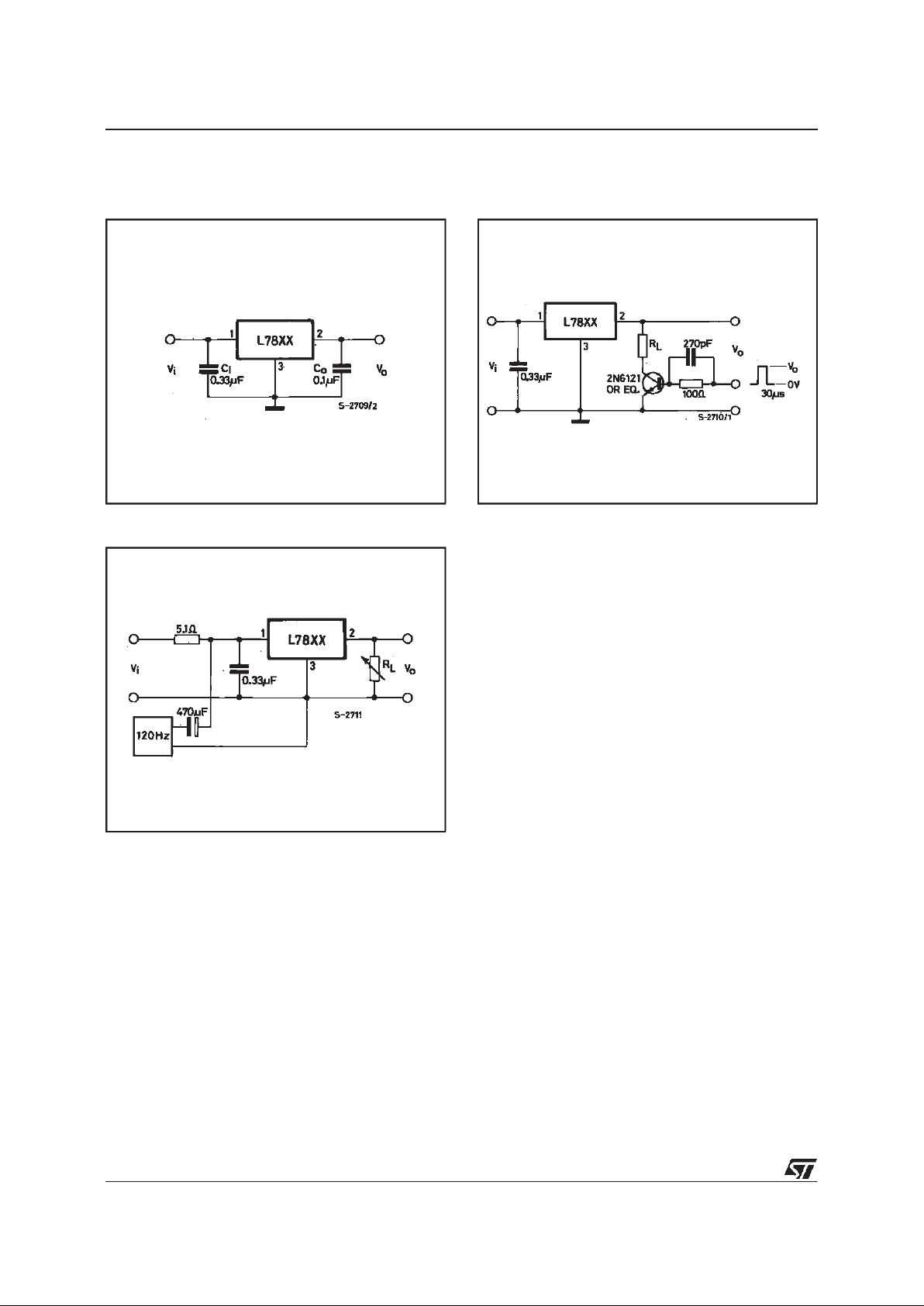
Figure4 :
CurrentRegulator.
Figure5 :
AdjustableOutput Regulator.
Figure6 : CurrentBoost Regulator. Figure 7 : Short-circuitProtection.
VO, 7.0V to 20V
V
i–VO
≥2.0V
The addition of an operational amplifier allows
adjustmentto higher or intermediate values while
retaining regulation characteristics. The minimum
voltage obtainable with this arrangement is 2.0V
greaterthan the regulatorvoltage.
The circuit of figure 6 can be modified to provide
supply protectionagainst shortcircuit by adding a
short-circuit sense resistor, R
sc
, and an additional
PNP transistor. The current sensingPNP must be
able to handle the short-circuit current of the
three-terminal regulator. Therefore, a
four-ampereplasticpower transistoris specified.
R1=
V
BEQ
1
I
REQ
−
I
Q
1
β
Q
1
IO=
I
REG
+
Q
1
(
I
REG
−
V
BEQ
1
R
1
)
I
O
=
V
XX
R
1
+
I
d
L7800AB/AC
14/17

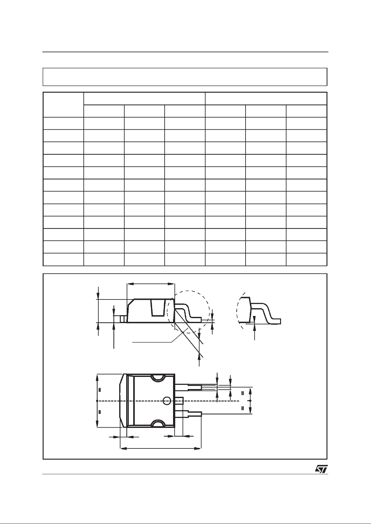
DIM.
mm inch
MIN. TYP. MAX. MIN. TYP. MAX.
A 4.40 4.60 0.173 0.181
C 1.23 1.32 0.048 0.051
D 2.40 2.72 0.094 0.107
D1 1.27 0.050
E 0.49 0.70 0.019 0.027
F 0.61 0.88 0.024 0.034
F1 1.14 1.70 0.044 0.067
F2 1.14 1.70 0.044 0.067
G 4.95 5.15 0.194 0.203
G1 2.4 2.7 0.094 0.106
H2 10.0 10.40 0.393 0.409
L2 16.4 0.645
L4 13.0 14.0 0.511 0.551
L5 2.65 2.95 0.104 0.116
L6 15.25 15.75 0.600 0.620
L7 6.2 6.6 0.244 0.260
L9 3.5 3.93 0.137 0.154
DIA. 3.75 3.85 0.147 0.151
L6
A
C
D
E
D1
F
G
L7
L2
Dia.
F1
L5
L4
H2
L9
F2
G1
TO-220 MECHANICAL DATA
P011C
L7800AB/AC
15/17
DIM.
mm inch
MIN. TYP. MAX. MIN. TYP. MAX.
A 4.4 4.6 0.173 0.181
A1 2.49 2.69 0.098 0.106
B 0.7 0.93 0.027 0.036
B2 1.14 1.7 0.044 0.067
C 0.45 0.6 0.017 0.023
C2 1.23 1.36 0.048 0.053
D 8.95 9.35 0.352 0.368
E 10 10.4 0.393 0.409
G 4.88 5.28 0.192 0.208
L 15 15.85 0.590 0.624
L2 1.27 1.4 0.050 0.055
L3 1.4 1.75 0.055 0.068
L2
L3
L
B2
B
G
E
A
C2
D
C
A1
DETAIL”A”
DETAIL”A”
A2
P011P6/F
TO-263 (D2PAK) MECHANICALDATA
L7800AB/AC
16/17

Information furnished isbelieved tobe accurate and reliable. However, STMicroelectronics assumes no responsibility for the consequences
of use of such information nor for any infringement of patents or other rights of third parties which may result from its use. No license is
granted by implication or otherwise under any patent or patent rights of STMicroelectronics. Specification mentioned in this publication are
subject tochange without notice. Thispublication supersedes and replaces all information previously supplied. STMicroelectronics products
are not authorized for use as critical components in lifesupport devices or systems withoutexpress written approval of STMicroelectronics.
The ST logo is a registeredtrademark of STMicroelectronics
1999 STMicroelectronics – Printed in Italy– All Rights Reserved
STMicroelectronics GROUP OF COMPANIES
Australia - Brazil - China - Finland -France - Germany - Hong Kong - India - Italy - Japan- Malaysia - Malta -Morocco
Singapore - Spain- Sweden - Switzerland - United Kingdom - U.S.A.
http://www.st.com
.
L7800AB/AC
17/17
 Loading...