


5V & 12V SPINDLE AND VCM MOTORS DRIVER
■
12V & 5V (±10%) OPERATION
■
REGISTER BASED ARCHITECTURE
■
3 WIRE SERIAL COMMUNICATION
INTERFACE UP TO 33 MHZ
■
BCD TECHNOLOGY
L7250
PRODUCT PREVIEW
Spindle Motor Controller
■
INTERNAL POWER DEVICE 0.9 OHM MAX
VALUE @ 125°C (SINK+SOURCE)
■
2.5A PEAK CURRENT CAPABILITY
■
ST SMOOTHDRIVE SINUSOIDAL PWM
COMMUTATION
■
DEDICATED ADC FOR POWER SUPPLY
VOLTAGE COMPENSAT IO N
■
SPINDLE CURRENT LIMITING VIA FIXED
FREQUENCY PWM OF SPINDLE POWER
OUTPUTS AT THE SMOOTHDRIVE PWM
RATE
■
SYNCHRONOUS RECTIFICATION DURING
PWM TO REDUCE POWER DISSIPATION
■
CURRENT SENSING VIA EXTERNAL
CURRENT SENSE RESISTOR
■
INDUCTIVE SENSE POSITION START UP
DRIVEN BY µPROCESSOR
■
SPINDLE BRAKING DURING POWER DOWN
CONDITION
Voice Coil Motor Driver with Ramp Load/Unload
■
INTERNAL POWER DEVICE 0.9 OHM MAX
VALUE @ 125°C (SINK+SOURCE)
■
2A PEAK CURRENT CAPABILITY
■
15 BIT LINEAR DAC FOR CURRENT
COMMAND, WITH INTERNAL REFERENCE
VOLTAGE
■
SENSE AMPLIFIER GAIN SWITCH
■
CLASS AB OUTPUT STAGE WITH ZERO
DEAD-BAND AND MINIMAL CROSSOVER
DISTORTION
■
RAMP LOAD AND UNLOAD CAPABILITY AS
WELL AS CONSTANT VOLTAGE RETRACT
■
EXTERNAL CURRENT SENSE RESISTOR IN
SERIES WITH MOTO R .
■
HIGH CMRR (>70DB) AND PSRR (>60DB)
SENSE AMP
■
EXTERNAL CURRENT CONTROL LOOP
COMPENSATION
■
HIGH BANDWIDTH VCM CURRENT
CONTROL LOOP CAPABI L ITY
■
HIGH PSRR, LOW OFFSET, LOW DRIFT GM
LOOP
ORDERING NUMBER: L7250
■
VCM VOLTAGE MODE, CONTROLLED BY
TQFP64
VCM DAC
■
GM LOOP OFFSET CALIBRATION SCHEME
INCLUDES A COMPAR ATOR ON THE
ERROR AMP
Auxiliary Functions
■
3.3V AND 1.8V LINEAR REGULATOR
CONTROLLER
■
NEGATIVE VOLTAG E REGUL ATOR
■
INTERNAL ISOFET 0.1 OHM @125C
■
POWER MONITOR OF 12V, 5V, 3.3V AND
1.8V
■
SHOCK SENSOR CIRCUIT TAKES INPUTS
FROM PIEZO OR CHARGING ELEMENT
■
10 BIT ADC WITH 4 MUXED INPUTS
■
THERMAL SENSE CIRCUIT AND OVER
TEMPERATURE SHUT DOWN
■
CHARGE PUMP BOOST VOLTAGE
GENERATOR FOR HIGH SIDE GATE DRIVE
■
ANALOG PINS AVAILABL E TO ENTER
SIGNALS TO BE CONVERTED BY THE
INTERNAL ADC
DESCRIPTION
L7250 is a power IC for driving the SPINDLE and
VCM motors, suitable for 5V & 12V application. The
spindle system includes integrated power FETs
which are driven using ST's Smoothdrive pseudo-sinusoidal commutation technology. The voice coi l motor (VCM) system includes integrated power FETs,
as well as ramp load and unload capability. Linear
3.3V and1.8V volt age regulators ar e include d, as wel l
as a negative regulator.
Power monitoring of VCC5, VCC12, and of the two
positive voltage regulators is also included.L7250
uses a 3 wire serial interface: S_DATA, S_CLK and
S_ENABLE
July 2001
This is preliminary information on a new product now in development. Details are subject to change without notice.
1/46
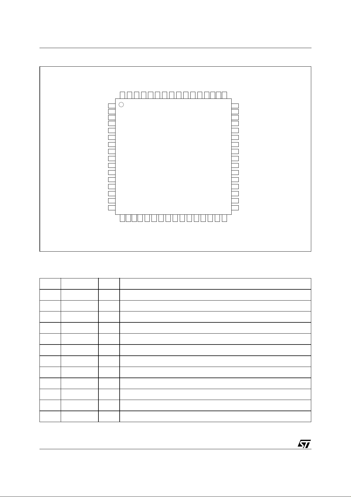
L7250
PIN CONNECTION
(Top view)
VCV1
VCV2
VCMP1
VCMP2
VCMGND1
VCMGND2
CPOSC
VCC5
DIG_GND
N_DRV
N_FEED
N_COMP
25_BASE
25_FEED
33_BASE
33_FEED
CT
OUTU1
RSEN4
VBOOST
64
01
02
03
04
05
06
07
08
09
10
11
12
13
14
15
16
OUTU2
CPOSCH
61
62
63
20212223242526272829303132
191718
RSEN3
60
59
58
VCV3
OUTV1
OUTV2
55
56
57
VCV4
VM1
VM2
53
54
Rsense
OUTW2
OUTW1
514950
52
RSEN2
48
RSEN1
47
VCMN2
46
VCMN1
45
VCMGND4
44
VCMGND3
43
SNS_N
42
SNS_P
41
SNS_OUT
40
ERR_OUT
39
ERR_IN
38
DAC_OUT
37
SCLK
36
SYSClk
35
SDATA
34
33
SEN
ZC
Skin
SkFin
CPOR
CBRAKE
VREF25
AGND
NPOR
Skout
SkFout
Timer1
SkDout
CalCoarse
PIN DESCRIPTI ON
N° Pin V Description
1 VCV1 S12 12V power supply
2 VCV2 S12 12V power supply and POR sensing threshold
3 VCMP1 O12 VCM positive output
4 VCMP2 O12 VCM positive output
5 VCMGND1 gnd VCM power ground
6 VCMGND2 gnd VCM power ground
7 CPOSC O12 Charge pump oscillator
8 VCC5 S5 5V power supply
9 DIG_GND gnd Digital & Switching regulator ground
10 N_DRV O5 Neg Reg ext FET gate driver
11 N_FEED I5 Neg Reg feedback
Test
ADaux
VCMBEMF
12 N_COMP IO5 Neg Reg error output
2/46
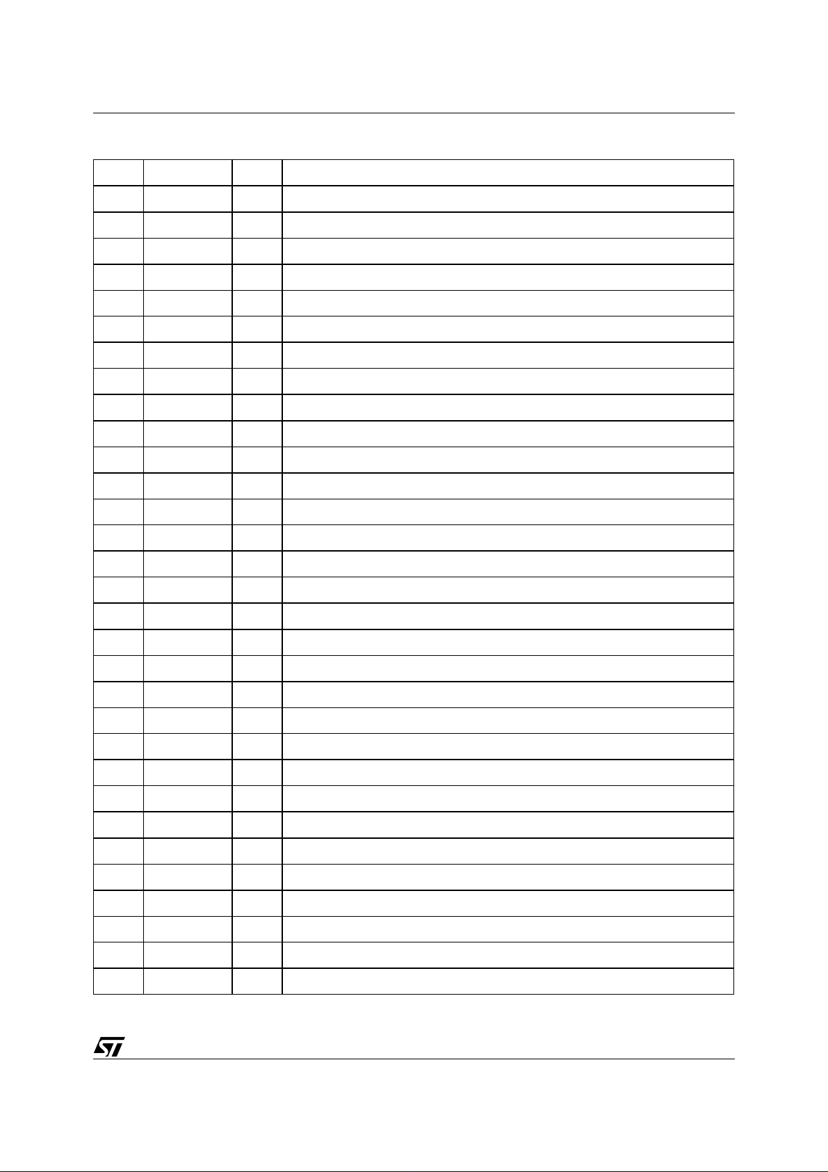
L7250
PIN DESCRIPTI ON
N° Pin V Description
13 25_BASE O5 Reg 1.8V ext NPN base
14 25_FEED I5 Reg 1.8V feedback
15 33_BASE O5 Reg 3.3V ext NPN base
16 33_FEED IO5 Reg 3.3 V feedback
17 CPOR IO5 POR delay capacitor
18 NPOR O5 POR output signal
19 CBRAKE IO5 Spindle brake capacitor
20 AGND gnd analog gnd
21 VREF25 IO5 2.5V reference
22 ZC O5 Spindle zero crossing
23 Skin I5 Shock sensor input
24 Skout O5 Shock sensor 1st opamp output
25 SkFin I5 Shock sensor filter input
26 SkFout O5 Shock sensor filter output
(continued)
27 SkDout O5 Shock sensor output
28 Timer1 IO5 Timer 1 for unload procedure
29 CalCoarse I5 VCM BEMF coarse calibration
30 ADaux I5 auxiliary input for the ADC
31 VCMBEMF O5 VCM BEMF processor output
32 Test IO5 used for testing porpouse (*)
33 SEN I5 Serial enable
34 SDATA IO5 Serial data
35 SYSClk I5 System clock
36 SCLK I5 Serial clock
37 DAC_OUT O5 VCM DAC output
38 ERR_IN I5 VCM error opamp input
39 ERR_OUT O5 VCM error opamp output
40 SNS_OUT O5 VCM sense opamp output
41 SNS_P I12 VCM sense opamp positive input
42 SNS_N I12 VCM sense opamp negative input
43 VCMGND3 gnd VCM power ground
3/46

L7250
PIN DESCRIPTI ON
N° Pin V Description
44 VCMGND4 gnd VCM power ground
45 VCMN1 O12 VCM negative output
46 VCMN2 O12 VCM negative output
47 RSEN1 O12 Spindle power sensing resitor
48 RSEN2 O12 Spindle power sensing resitor
49 Rsense I5 Spindle sensing resistor input
50 OUTW1 O12 Spindle phase C output
51 OUTW2 O12 Spindle phase C output
52 VM1 IO12 Vmotor
53 VM2 IO12 Vmotor
54 VCV4 S12 12V power supply
55 VCV3 S12 12V power supply
56 OUTV1 O12 Spindle phase B output
57 OUTV2 O12 Spindle phase B output
(continued)
58 RSEN3 O12 Spindle power sensing resitor
59 RSEN4 O12 Spindle power sensing resitor
60 OUTU1 O12 Spindle phase A output
61 OUTU2 O12 Spindle phase A output
62 CT I12 Spindle central tap
63 CPOSCH IO20 Charge pump diodes connection
64 VBOOST IO20 Charge Pump voltage
(*) used al so to set the IC power supply applicati on. If this pin is pull-up exter nal l y the L7250 be came a 5V appl i cation
S = Supply ; IO = Input/Output ; I = Input ; O = Output ; gnd = Ground.
4/46

ELECTRICAL CHARACTERISTCS
ABSOLUTE MAXIMUM RATINGS
Symbol Parameter Value Unit
VCV1,VCV2,VCV3,VCV4 14 V
VCC5 maximum voltage 6 V
L7250
OUTU1,OUTU2,OUTV1,OUTV2,OUTW1,OUTW2
VCMP1,VCMP2,VCMN1,VCMN2
VM1,VM2
Digital Input Voltage -0.3 to VCC5 V
Operating free-air temperature 0 to 70 °C
Storage Temperature -55 to 150 °C
-1V to 16 V
ELECTRICAL CHARACTERISTCS
POWER SUPPLY [VCC5 & VCV] VCC5 = 5V ±10%, VCV = 12V ±10%. T
Symbol Parameter Test Condition Min. Typ. Max. Unit
POWER MONITOR, SUPPLY CURRENTS, ETC.
Icc5 VCC5 Operating current Spindle and VCM enabled, no
load
Ivcv VCV + VRET Operating current Spindle and VCM enabled, no
load
CHARGE PUMP VOLTAGE BOOSTER
VBOOSTCharge pump output voltage VCV = 12V
Iload = 5mA
= 25°C (unless otherwise specified)
amb
9mA
44 mA
18.5 V
VBOOS
Tfreq
POWER MONITOR
vt5 VCC5 threshold 4.0 4.175 4.35 V
vt12 VCC12 threshold 9 9.5 10 V
hv5 VCC5 hysteresis 40 100 160 mV
hv12 VCC12 hysteresis 100 200 300 mV
vt33 V33 Threshold 2.7 2.8 2.9 V
hv33 V33 Hysteresis 20 40 60 mV
vt18 V18 Threshold (at pin 25_FEED) 1.07 1.12 1.17 V
hv18 V18Hysteresis 25 50 75 mV
NPOR
Switching frequency 1 MHz
NPOR low level output voltage VCV > 4.5V Iol = 5mA 0.75 V
low
5/46
L7250
ELECTRICAL CHARACTERISTCS
POWER SUPPLY [VCC5 & VCV] VCC5 = 5V ±10%, VCV = 12V ±10%. T
(continued)
= 25°C (unless otherwise specified)
amb
Symbol Parameter Test Condition Min. Typ. Max. Unit
NPOR
NPOR internal pull_up resistor to
pull
6Kohm
V33
CPOR
CPOR
CPOR charging current Vout = 0V 5 uA
Ic
CPOR low level output voltage VCV > 4.5V Iol = 1mA 50 mV
low
Vref25 2.5V reference voltage -5% 2.5 +5% V
THERMAL WARNING AND THERMAL SHUTDOWN
T
warn
Thermal warming temperature Characterized, tested by
130 140 150 °C
correlation.
Tsoff Thermal Shutdown temperature Characterized, tested by
150 165 180 °C
correlation
Thys Thermal Hysteresis valid for both temperature
20 25 30 °C
thresholds
VM ISOLATION FET
IsoR Rds ON @ 125°C , I=2.5A 0.1 Ohm
IsoI Continuous current 2.5 A
SPINDLE DRIVER SECTION
POWER STAGE
Rds(on) Total output ON resistance
@ 125°C, I=2.5A 0.9 Ω
(Source + Sink)
Idsx Output leakage current -200 -500 µA
CTlkg Centarl tap leakage 1 µA
DiodeFw Clamp diode forward voltage If = 2.5A 0.6 1.2 V
Slew Output slew rate OUTx 10% to 90%
40 V/µS
Reg04H ‘b7b6b5’ = 011
BACK EMF COMPARATOR
Vie Common mode input voltage
Guaranteed by design 0 VM V
range.
Vr Input voltage range where output
Guaranteed by design -1 VM+1 V
shall not invert.
BEMFoff BEMF input offset CT = 6V -15 +15 mV
BEMFhy BEMF hysteresys CT = 6V 50 mV
SPINDLE CURRENT LIMITING
Iin RSENSE Input bias current. 0 < Vin < 3.3V 1 µA
CURoff Comparator offset -15 +15 mV
6/46
L7250
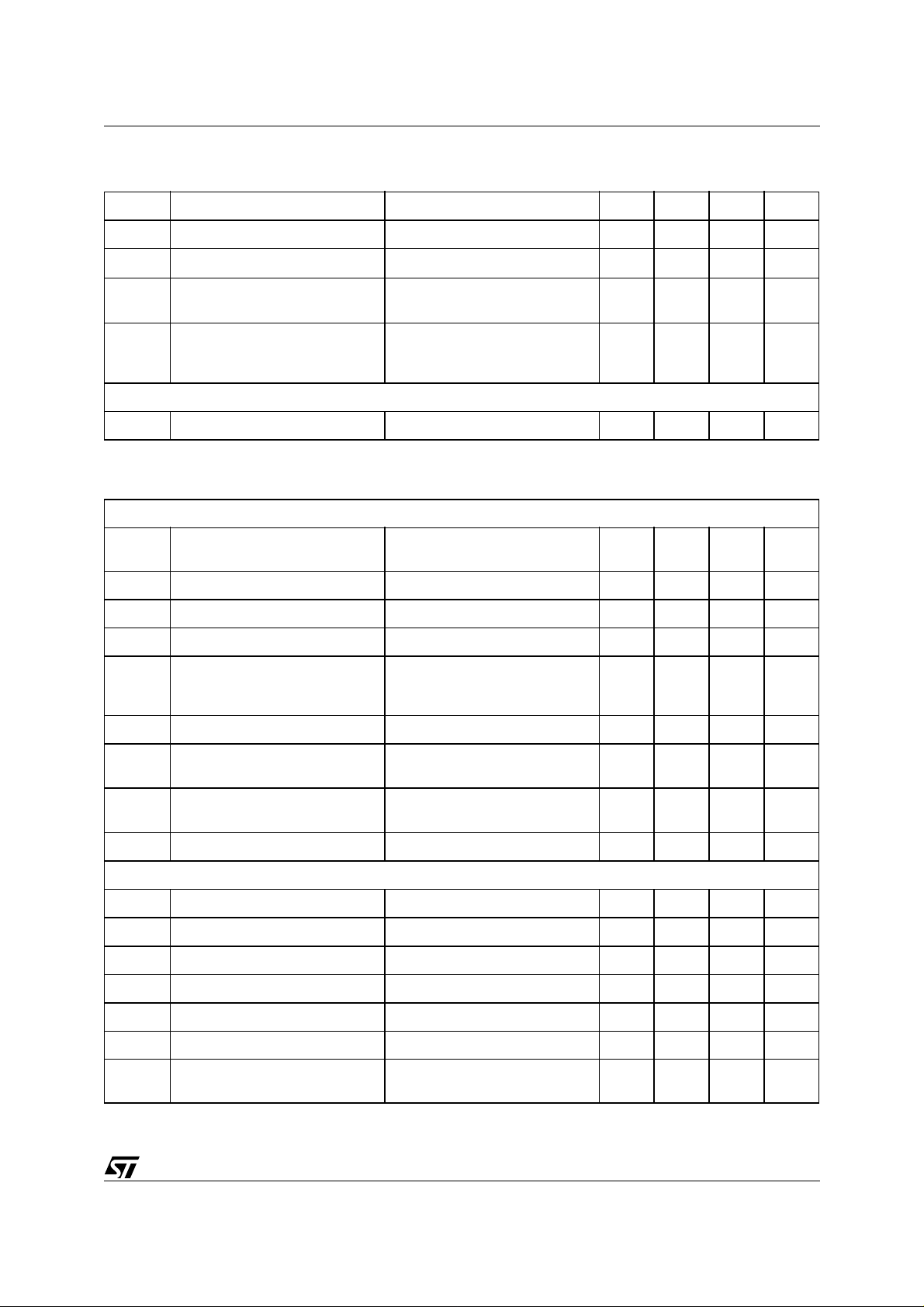
ELECTRICAL CHARACTERISTCS
POWER SUPPLY [VCC5 & VCV] VCC5 = 5V ±10%, VCV = 12V ±10%. T
(continued)
= 25°C (unless otherwise specified)
amb
Symbol Parameter Test Condition Min. Typ. Max. Unit
CURdacr
CUR
CUR
CUR
DAC resolution 3 bit
DAC output Reg04H ‘b4b3b2’ = 000 250 mV
dac_L
DAC output Reg04H ‘b4b3b2’ = 111 600 mV
dac_H
DAC linearity -10 +10 mV
lin
Cbrake
Icbrake VCbrake leakage VCbrake=5V 1 µA
VCM SECTION
CURRENT SENSE AMPLIFIER
Vts Common mode input voltage
GBD - not tested -0.6 VM+1 V
range.
Sns _vof
Sns_gai n0
f Input offset voltage -12 12 mV
Differential Voltage GAIN0 Reg09H ‘b7’ = 0 -5% 4.5 +5%
Sns _gain1
Sns_low
Sns_high
sns_slew
Sns_band
sns _cmrr
sns _svrr
Differential Voltage GAIN1 Reg09H ‘b7’ = 1 -5% 16 +5%
VSENSE output saturation
voltage
Iload=+/-1mA
Vin_diff=+/- 500m V
4.75
250 mV
V
Output slew rate Cload=50pF 1 V/µs
-3dB Bandwidth Guaranteed by design 200 400 kHz
Common mode rejection ratio f < 10 KHz, tested at DC only
CMRR=A
V DIFF/AV CM
70 dB
supply voltage rejection ratio VCV f < 10 KHz, tested at DC only 60 dB
ERROR SUMMING AMPLIFIER
err _gain Voltage gain no load 60 dB
err _band
Unity gain bandwidth Guaranteed by design 4 MHz
err _slew Output Slew Rate Cload=50pF 1.5 V/µS
err _ibias
Input bias current 1 µA
err _off Input offset voltage -10 0 10 mV
err_svrr supply voltage rejection ratio f < 10 KHz, tested at DC only 60 dB
err _clamp
Low output (clamp) voltage Isink = 1 mA, referred to Vref25 TBD V
low
7/46
L7250
ELECTRICAL CHARACTERISTCS
POWER SUPPLY [VCC5 & VCV] VCC5 = 5V ±10%, VCV = 12V ±10%. T
Symbol Parameter Test Condition Min. Typ. Max. Unit
err _clamp
high
VCM OUTPUT DRIVERS
PWR_Gain
Rds(on) Total output ON resistance
PWR_Lkg
DiodeFw Clamp diode forward voltage If = 2A 0.6 1.2 V
THD Total Harmonic Distortion characterized no tested 1 %
PWR_Slew
PWR_B
and
Icross Static Shoot-through current Guaranteed by design 0 mA
VCM CURRENT CONTROL LOOP STATIC AND DYNAMIC CHARACTERISTICS
IVCMoff Total offset current Rs=0.2 -75 75 mA
High output (clamp) voltage Isource = 1mA, referred to Vref25 TBD V
Power amplifier differential gain. Io = ±1A, Rload = 8Ω 14 15 16 V/V
(Source + Sink)
Output leakage current 600 uA
VCMN or VCMP slew rate RL = 8 ohms 1 V/us
Power Amp -3dB Bandwidth Driving ERROUT = VDACREF,
(continued)
@ 125°C, I=2A .9 Ω
Guaranteed by design
= 25°C (unless otherwise specified)
amb
250 500 kHz
DIVCMoff
Gm_psrr Gm loop VSRR of VCV -1 1 mA/V
VCM LINEAR DAC
DAC_res Resolution 15 bit
DAC_out Full Scale Output Voltage wrt VDACREF 0.96 1 1.04 V
DAC_off Mid-Scale Error wrt VDACREF -12 12 mV
DAC_DNL
DAC_INL
DAC_Co
nvT
VCM LOAD/UNLOAD
ADC
ADC_res
ADC_DNL
ADC_INL
Total offset current drift
temperature coefficient
Differential Non linearity Guaranteed Monotonicity ±1 LSB
Integral Non Linearity ±64 LSB
Conversion time 90% from 3FFFh to 0020h 3 µs
resolution 10 bit
Differential Non Linearity 1 LSB
Integral Non Linearity 3 LSB
Guaranteed by design .2
mA/oC
ADC_Co
nvT
8/46
Conversion time 40 ADC
Clock
cycles
L7250
ELECTRICAL CHARACTERISTCS
POWER SUPPLY [VCC5 & VCV] VCC5 = 5V ±10%, VCV = 12V ±10%. T
Symbol Parameter Test Condition Min. Typ. Max. Unit
ADC AUXILIARY INPUT
AUX_ran
ge0
AUX_ran
ge1
AUX_Ibias
VCM VOLTAGE AMPLIFIER
V olt_gain
Volt_off Input offset -15 +15 mV
Vo lt
_cmrr
Volt
_svrr
BEMF processor amplifier
CalCoar
seIn
Input range 0 Reg06H ‘b3’ = 0
Input range 1 Reg06H ‘b3’ = 1
Input bias -100 100 µA
Voltage gain 0.165 V/V
Common mode rejection ratio f < 10 KHz, tested at DC only
supply voltage rejection ratio f < 10 KHz, tested at DC only 60 dB
Calcoarse voltage input range 0.5 2 V
(continued)
Referred to Vref25
Referred to Vref25
CMRR=A
V DIFF/AV CM
= 25°C (unless otherwise specified)
amb
±1 V
±2.25 V
46 dB
Gain1 First stage gain Vcontrol = 1.25 V 1.91 V/V
Gain2 Second stage gain 16 V/V
Offset Residual input offset after
calibration
Rout BEMF amp output resistance (pin
31)
ULOAD @ POR
Timer1_V
Timer1_I Timer1 Discharging Current 2 µA
Timer1_T
VOLTAGE REGULATORS
1.8 AND 3.3 LINEAR REGULATOR
V18 feed 1.8V feedback Voltage -5% 1.25 +5% V
V33 OUT
Timer1 Charging Voltage 2.5 V
Timer1 Low threshold 0.2 V
3.3V Output Voltage -5% 3.3 +5% V
Vcontrol = 1.25V
(Measured between VCMN and
SNS_P pins)
-3 +3 mV
500 ohm
9/46
L7250
ELECTRICAL CHARACTERISTCS
POWER SUPPLY [VCC5 & VCV] VCC5 = 5V ±10%, VCV = 12V ±10%. T
Symbol Parameter Test Condition Min. Typ. Max. Unit
V18
IDRIVE
V33
IDRIVE
NEGATIVE REGULATOR
FREQ0 Oscillator frequency Default configuration 500 KHz
FREQ1 Oscillator frequency TestRegister = ‘00001001’
VoutH High level output voltage TBD V
VoutL Low level output voltage TBD V
VNEerr
OFFS
VNEGerr
BIAS
Vneg_err
_cmrr
Vneg_err
_svrr
Output base current drive
Feedback input offset -10 10 mV
Feedback input bias 0 1 µA
Common mode rejection ratio f < 10 KHz, tested at DC only
supply voltage rejection ratio VCV f < 10 KHz, tested at DC only 60 dB
(continued)
or = ‘00101001’
CMRR=A
V DIFF/AV CM
= 25°C (unless otherwise specified)
amb
1 MHz
46 dB
15 mA
SHOCK SENSOR
SkIgain0 Input OPAMP gain0 Reg02H ‘b7’ = 0 10 V/V
SkIgain1 Input OPAMP gain1 Reg02H ‘b7’ = 1 80 dB
SkIoff Input OPAMP offset -15 +15 mV
SkIinput Input OPAMP input impedance Reg02H ‘b7’ = 0 10 Mohm
SkFgain Filter OPAMP open loop gain 80 DB
SkFband Filter OPAMP unity gain
bandwidth
SkFoff Filter OPAMP offset voltage -10 +10 MV
SkOThH0
SkOThH1
SkOThL0
SkOThL1
Output window comparator
VthHigh
Output window comparator
VthHigh
Output window comparator
VthLow
Output window comparator
VthLow
Guaranteed by design 5 Mhz
Referred to Vref25 ;
Reg02H ‘b6’ = 0
Referred to Vref25 ;
Reg02H ‘b6’ = 1
Referred to Vref25;
Reg02H ‘b6’ = 0
Referred to Vref25;
Reg02H ‘b6’ = 1
200 mV
500 mV
200 mV
500 mV
10/46

L7250
ELECTRICAL CHARACTERISTCS
POWER SUPPLY [VCC5 & VCV] VCC5 = 5V ±10%, VCV = 12V ±10%. T
Symbol Parameter Test Condition Min. Typ. Max. Unit
SERIAL PORT
Voh Logic Output voltage high Ioh=1mA 2.7 V
Vol Logic Output voltage low Iol=1mA 0.5 V
Vih L ogic input high Iih=1uA 2.2 V
Vil Logic input low Iil=-1uA 0.5 V
Iih Logic high input current Internal Pulldown Resistor
Iil Logic low input current -1.00 µA
(continued)
Vin = 3.3V
= 25°C (unless otherwise specified)
amb
33 µA
1 SERIAL PORT
The serial port is a bidirectional three pi n interface, using SDATA, SCLK and SE N to addr ess and communi cate
with sixteen 8 bit registers in the L7250. These registers include the status register, Spindle control registers,
VCM control registers, sinewave drive registers, and test mode register. These registers are cleared to zero at
power up.
1.1 Default comunication modes setting (bit 7, Reg05H ) = 0
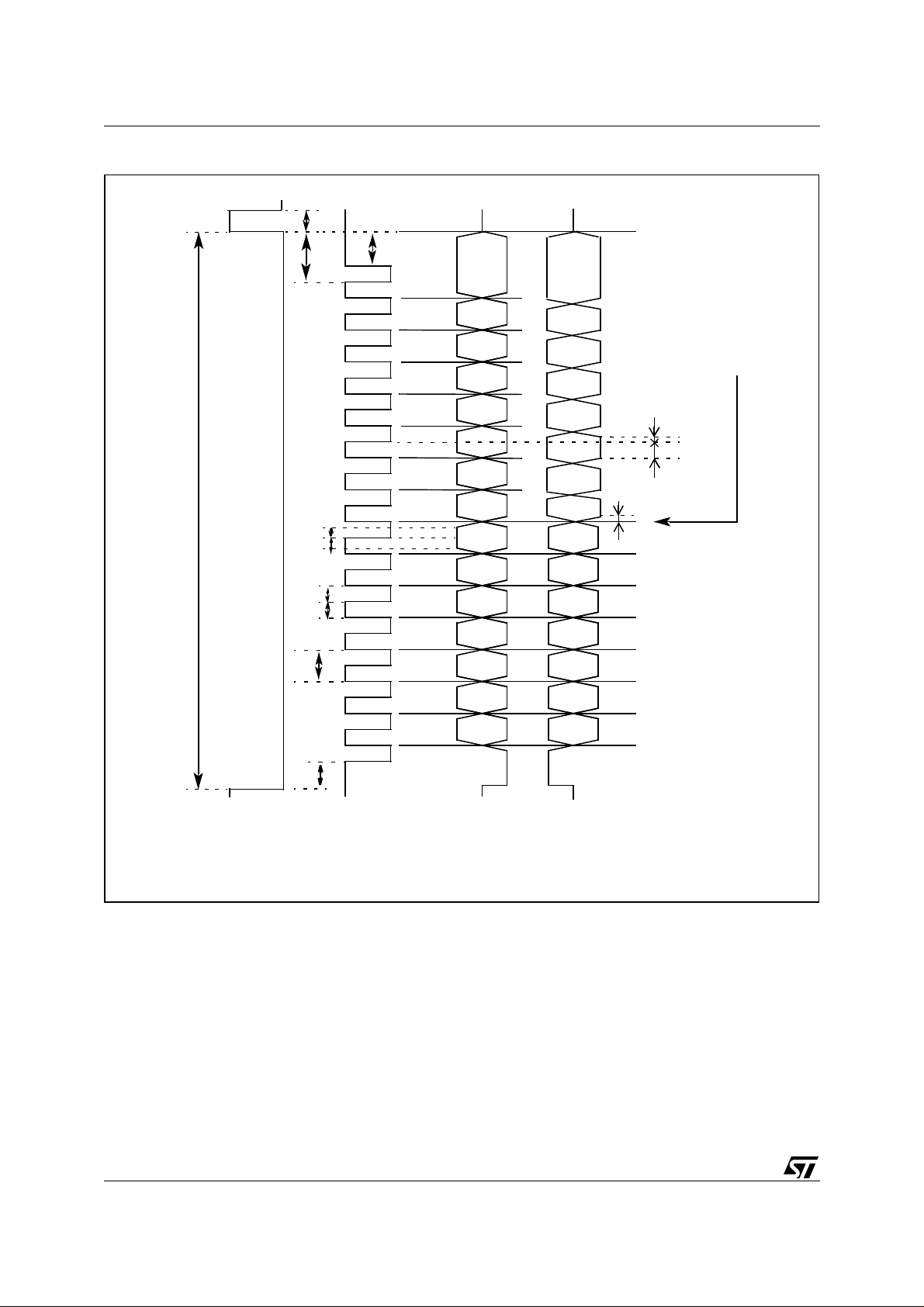
After the SEN falling edge, the internal state machine is waiting for the first SCLK falling edge. This means that
if the SCLK line starts from an high level the first falling edge, respecting the setup time Tefcf, is considered,
and is used to read the R/W bit. During a writing process the internal state machine must see 16 SCLK falling
edges to validate the operation. The write mode is started if the R/W bit is low on the first falling edge of SCLK.
The read mode is started if the R/W bit is high on the first falling edge of SCLK. The ID, Address, and Data are
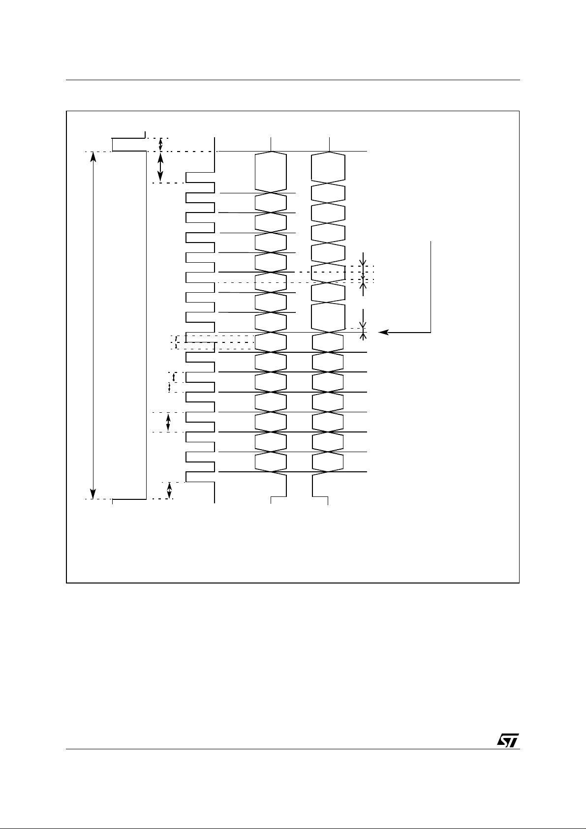
all then subsequently read by the L7250 on the falling edges of SCLK. (See Figure 1)
The microcontroller has to read the data on the falling edge of the SCLK signal. After the hold time (Tedh) the
data line switches to the next data without a tri-state phase.During a read mode the last address bit is read by
L7250 on the eighth falling edge of SCLK. The internal state machine then turns the SDATA bit around for the
L7250 to assume control at the next SCLK rising edge (the first rising edge after the 8th SCLK falling edge).
11/46
L7250
Figure 1. Default serial port timing diagram (bit 7, Reg05H = 0)
Teh
Tcfer
Tcrer
D1 D0
D2
D0
Tedh
D5 D4 D3
D6
D6 D5 D4 D3 D2 D1
D7
Tdly
Tcdd
L 7250 takes bus control
Tcds Tcdh
A1 A0 D7
A2
A1 A0
A2
Tcc Tch Tcl
ID2 ID2 A2
ID2 ID2 A2
ID 2
Tefcf
SEN
Note1: During writing process L7250 latches the data on the SC LK falling edge (the ASI C is writing on the SCLK
rising edge)
Note2: During reading process L7250 takes the bus control on the next SCLK rising edge after the 8th SCLK
falling edge
The L7250 write the data on the SCLK falling edge respecting the data hold time (Tedh)
Note3: The ID number for the L7250 is ID1=ID2=ID3=1
12/46
SCLK
W
SDATA
(w rite)
ID 2
R
SDATA
(read)
1.2 Default serial port timing Table
Symbol Parameter Min Max Unit
Tcc Serial clock period 30 ns
Tch Serial clock high time 13 ns
Tcl Serial clock low time 13 ns
Tcds Serial data setup time to clock falling edge (write mode) 5 ns
Tcdh Serial clock falling edge to serial data hold time (write mode) 4 ns
Tedh Serial clock falling edge to serial data hold time (read mode) 5 ns
Tcdd Serial data setup time to clock falling edge (read mode) 5 ns
Tel Serial Enable low time 490 ns
Teh Serial Enable high time 30 ns
Tefcf Serial Enable falling edge to serial clock falling edge 17 ns
Tcfer Serial clock falling edge to Serial enable rising edge 17 ns
Tdly SDATA turn around delay time 0 ns
L7250
Note 1: All specifications with respect to 50% of signal switching thresholds
Note 2: Reading mode tested at M ax 20Mhz
1.3 Inverted clock comunication modes (bit 7, Reg05H) = 1
To set the bit7, Reg05H to 1, entering this different comunication mode, a writing process using the default comunication protocol (see the above paragraph) must be used.
After the SEN falling edge, the internal state machine is waiting for the first SCLK rising edge. This means that
if the SCLK line starts from a low level the first rising edge, respecting the setup time Tefcr, is considered, and
is used to read the R/W bit. The internal state machine must see 16 SCLK rising edges to validate the write
operation. The write mode is started if the R/W bit is low on the first rising edge of SCLK. The read mode is
started if the R/W bit is h igh on the first rising ed ge of SCLK. The ID, Address, and Data are a ll then subsequently read by the L7250 on the rising edges of SCLK (See Figure 2).
The microcontroller has to r ead (l atch) the data on the falli ng edge of the SCLK signal. L7250 pr esents the data
on the SCLK rising edge. During a read mode the last address bit is latched by the L7250 on the eighth rising
edge of SCLK. The internal state machine then turns the SDATA bit around for the L7250 to ass ume control at
the next SCLK falling edge (the first falling edge after the 8th SCLK rising edge).
13/46
L7250
Figure 2. Inverted clock serial port timing diagram (bit 7, Reg05H = 1)
Teh
Tcrer
D1 D0
D2
D0
Tedh
D5 D4 D3
D6
Tel
D6 D5 D4 D3 D2 D1
D7
Tdly
Tvld
L7250 takes bus control
Tcdh
Tcds
A1 A0 D 7
A1 A0
Tcl
A2
A2
Tch
Tcc
ID 2 ID2 A2
ID 2 ID2 A2
ID 2
Tefcr
SEN
Note1: During writi ng proc ess L7250 l atches the data on the SCLK ris ing ed ge ( the ASIC is w riting on the S CLK
falling edge)
Note2: During reading proces s L7250 takes the bus c ontrol on the next SCLK falling edge after the 8th SCLKrising edge
The L7250 write the data on the SCLK rising edge and it is expec ting the ASIC to latches the data on the SCLK
falling edge
Note3: The ID number for the L7250 is ID1=ID2=ID3=1
14/46
SCLK
W
SDATA
(w rite)
R
SDATA
ID 2
(read)
 Loading...