

SMOOTH DRIVE SYSTEM
1.8A DRIVE PEAK CAPABILITY
SLEW RATE CONTROL
INDUCTIVE SENSE START-UP ROUTINE
THERMAL SHUTDOWN
SUITABL E FOR 5V AND 12 V APPLIC AT ION
ONLY ONE HALL SENSOR IS REQUIRED
DESCRIPTION
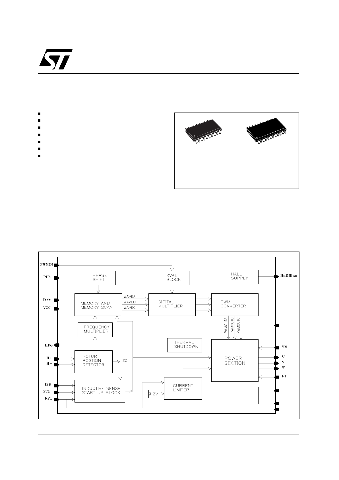
The L7203 SPINDLE MOTOR IC includes a three
phase brushless spindle motor controller and the
power stage in switching mode. The device is designed for both 5V and 12V OPTICAL DRIVE application requiring up to 1.8A peak of current.
The device is realized in BCD5, a 0.7 µm Mixed
technology.
The spindle motor position detection is carried
out by means of a single comparator with hysteresis. In the start-up phase the "inductive sense
start up method" is used to detect the rotor position, determining the direction of starting rotation.
This procedure is implemented by a logic circuit
on chip.
The device applies three sinusoidal voltages to
the motor coils.
This is obtained through the application of the
April 2001
LOW VOLTAGE
DETECTO
R
PRS
SRC
AGND
DGND
BLOCK DIAGRAM
ORDERING NUMBERS: L7203 (SO20)
L7203S (SSO24)
L7203
SMOOTH DR IVE SPI NDLE M OTO R FOR OPTI CAL DRI VE
APPLICATION WITH POWER INTEGRATED
®
SO20
SSO24
1/13

SMOOTH DRIVING concept.
It is based on the idea of driving the motor wind-
ing through 3 sinusoidal voltages dephased of
120 degrees. The motor is controlled in voltage
mode, so no current control compensation network is required.
Each profile is digitally described by 36 bytes
stored in a ROM memory.
These sinusoidal signals are modulated by multiplying each sample by a value stored in the KVAL
register. Using this kind of profiles it is possible to
obtain great advantages such as torque ripple
and acoustic noise reduction and lower EMI. An
easier track following is ensured, since vibration
are reduced.
The clock signal on the chip can be synchronized
to the external application clock signal.
An internal circuit can limit the current. The
threshold is fixed with a internal 0.2 V reference.
The device generates:
- a current generator to define output voltage
slew rate
- a 3.3 V reference to bias hall sensor.
- the HFG open drain output signal for speed
regulation.
The device includes :
- a circuit for thermal shutdown with hysteresis.
- a low voltage detector
In the STANDBY state the main functions of the
device are turned off, in order to minimize the
power consumption.
The STANDBY state of the device is imposed by:
- Thermal shutdown
- stand by signal from µP
PIN CONNECTIONS
DESCRIPTION
(continued)
PRS
N.C.
N.C.
VM
U
N.C.
V
W
RF H BIAS
ISR
V
CC
DGND
AGND
SRC
HFG
FSYS
STB1
3
2
4
5
6
7
8
9
22
21
20
19
18
16
17
15
23
10
24
N.C. PHS
D01IN1174
RF1 PWMIN11 14
1312H+ H-
STB
PRS
VM
U
V
RF
W
RF1
H+ PHS
HBIAS
ISR
AGND
VCC
DGND
SRC
HFG
FSYS1
3
2
4
5
6
7
8
9
18
17
16
15
14
12
13
11
19
10
20
H- PWMIN
D98IN928A
SO20
SSO24
L7203
2/13

PIN DESCRIPTION
PIN DESCRIPTION TYPE
POWER AND GROUND
VM Supply voltage for power stages +12/5V P12
VCC Supply for 5V core P5
DGND Logic ground G
AGND Analog ground G
DIGITAL PIN
PWMIN PWM input signal to calculate kval IC5
Fsys System frequency IC5
PHS Phase Shift Pin IC5
PRS Prescaler Pin IC5
STB Start and Stop signal ZD5
HFG Open Drain F-Generator signal from Spindle Motor OD5
HALL SENSOR
BIAS 3.3V reference to bias Hall sensor OA5
H+, H- Hall sensor differential input IA5
INDUCTIVE SENSE REFERENCE
ISR Inductive sense reference IA5
MOTOR CONTROL
OUTV Winding output U OA12
OUTV Winding output V OA12
OUTW Winding output W OA12
RF Current sense resistor (force) OA12
RF1 Current sense resistor (sense) IA5
SLEW RATE CONTROL
SRC Slew Rate Control OA5
INPUT DEFINITION
IC5 Input CMOS, 3.3-5V capability with hysteresis
ZD5 Bidirectional, open drain, 3.3-5V capability
OD5 Output, open drain, 3.3-5V capability
IA5 Input, Analog, 5V
OA5 Output, Analog, 5V
OA12 Output, Analog, 12V
P12 Power 12V / 5V
P5 Power 5V
G Ground
L7203
3/13

DC ELECTRICAL CHARACTERISTICS
( V
CC
= 5V; VM = 12V; T
amb
= 25°C unless otherwise specified)
Symbol Parameter Test Condition Min. Typ. Max. Unit
SUPPLY
V
CC
Supply 5V operating range 4.25 5.75 V
V
M
Supply 12V operating range (note 1) 10.2 13.8 V
V
M
Supply 5V operating range 4.25 5.75 V
I
Vcc
VCC Supply Current VCC = 5.75; f
sys
= 20MHz STB = 0
(bias pin open) STB =1
1.3
20
mA
mA
V
VM
VM Supply Current VM = 13.8 S TB = 0
STB =1
1
7
mA
mA
PWMIN, PHS, PRS, Fsys
V
iL
Input Low Voltage 1 V
V
iH
Input High Voltage 2.2 V
V
iHYS
Input Hysteresis 100 mV
I
z
Leakage Current VCC = 5.75 -10 +10 µA
STB
V
iL
Input Low Voltage 1 V
V
iH
Input High Voltage 2.2 V
V
OL
Open Drain Output IOL = 2mA VCC = 4.25V 0.4 V
V
iHYS
Input Hysteresis 100 mV
I
z
Leakage Current VCC = 5.75, Therm off -10 +10 µA
HFG
V
OL
Open Drain Output IOL = 2mA VCC = 5V 0.4 V
I
z
Leakage Current VCC = 5.75, HFG hiz -10 +10 µA
THERMAL DATA
Symbol Parameter Value Unit
R
th j-pins
Thermal Resistance Junction to Pins Max. 16 °C/W
R
th j-amb
Thermal Resistance Junction to Ambient Max. 90 °C/W
ABSOLUTE MAXIMUM RATINGS
Symbol Parameter Value Unit
T
amb
Ambient Temperature -20 to 80 °C
T
op
Operating Temperature 0 to 150 °C
T
smin
Minimum Thermal Circuit Threshold 140 °C
V
M
-0.3 to 15 Vdc
V
CC
-0.3 to 7 Vdc
U, V, W, (low side drive =off) -0.3 to 17 Vdc
PWMIN, PHS, FSYS, TEST, STB, HFG, BIAS, H+, H-, RF1,
RF, ISR, PORPin
-0.3 to V
CC
+0.3 Vdc
P
D1
Power dissipation at sustained operation with a package R
thj-amb
at 90°C
1W
ESD Susceptibility 2000 Vac
T
STG
Storage Temperature -55 to 150 °C
I
OLHFG
HFG open drain current 10 mA
I
Peak
Motor Peak Current 1.8 A
L7203
4/13
 Loading...