L7200
MOZART, 12V DISK DRIVE SPINDLE & VCM, POWER &
CONTROL “COMBO”
PRODUCT PREVIEW
GENERAL
■
12V (+/- 10%) OPERATION.
■
REGISTER BASED ARCHITECTURE
■
MINIMUM EXTERNAL COMPONENTS
■
BCD TECHNOLOGY
VCM DRIVER
■
1.7A DRIVE CAPABIL ITY
■
0.75Ω TOTAL BRIDGE IMPEDANCE AT 125°C
■
LINEAR MODE
■
PHASE SHIFT MODULATION (PWM MODE)
■
INSTANTANEOUS, (GLICH FREE) SWITCH
■
BETWEEN THE 2 MODES.
■
CLASS AB OUTPUT DRIVERS
■
ZERO CROSSOVER DISTORSION
■
14 BIT DAC DEFINE OUTPUT CURRENT
■
SELECTABLE TRANSCONDUCTANCE
■
RAMP LOADING & PARKING VOLTAGE
■
FULL INTERNAL VCM CALIBRATION
■
DYNAMIC BRAKE
SPINDLE DRIVER
■
2.5A DRIVE CAPABIL ITY
■
0.75Ω TOTAL BRIDGE IMPEDANCE AT
125°C
■
SMOOTHDRIVE™ ARCHITECTURE
■
SINUSOIDAL DRIVING, VOLTAGE MODE
■
BIPOLAR DRIVING
■
BEMF, INTERNAL OR EXTERNAL,
PROCESSING
■
SENSOR-LES S MOTOR COM MUTA TION
■
PROGRAMMABLE COMMUTATION DELAY
■
FIXED FREQUENCY PW M OPERATION
MODE
■
INTERNAL FREQUENCY LOCKED LOOP
SPEED CONTROL (FLL)
■
PROGRAMMABLE DIGITAL FILTER FOR
SPEED CONTROL LOOP
■
BEMF RECTIFICATION DURING RETRACT
■
BUILT-IN INDUCTIVE SENSING START UP
■
DYNAMIC & REVERSE BRAKE
■
BACK ROTATION DETECTION
MULTIPOWER BCD TECHNOLOGY
TQFP64
ORDERING NUMBER: L7200
OTHER FUNCTIONS
■
12V, 5V , 3.3V AND 2.5V MONITORING WITH
POSSIBLE EXTERNAL SET TRIP POINTS
AND HYSTERESIS
■
POWER UP/DOWN SEQUENCING
■
8V, 3.3V AND 2.5V POSITIVE REGULATORS
■
3.3V LOGIC COMPATIBILITY
■
SHOCK SENSOR DETECTOR
■
INTERNAL POR DELAY TIME AT POWER ON
(80ms)
■
INTERNAL ISOFET FOR BEMF
RECTIFICATION
■
THERMAL SHUTDOWN AND PRETHERMAL
WARNING
DESCRIPTION
The L7200 Mozart integrates into a single chip both
spindle and VCM controllers as well as power stages. The device is designed for 12V disk drive application requiring up to 2.5A of spindle and 1.7A of
VCM peak currents. The device is based on the sinusoidal driving of the spindle motor. This is realized
digitally by the SMOOTHDRIVE™ SYSTEM.
A serial port with up to 40 MHz capability provides
easy interface to the microprocessor. A register controlled Frequency Locked L oop (FLL) allow s flexibili ty
in setting the spindle speed. Integrated BEMF processing, digital filter, digital masking, digital delay,
and sequencing minimize the number of external
components required.
September 1999
This is preliminary information on a new product now in development. Details are subject to change without notice.
1/23
L7200
g
g
g
DESCRIPTION
(continued)
Power On Reset (POR) circuitry is included. Upon detection of a low voltage condition, POR is asserted, the
internal registers are reset, and spindle power circuitry is tri-stated. The BEMF is rectified providing power for
actuator retraction followed by dynamic spindle braking. Three Linear regulators and a Shock Sensor circuitry
are also integrated.
The device is built in BCD mixed signal technology allowing dense digital/analog circuitry to be combined with
a high power DMOS output stage.
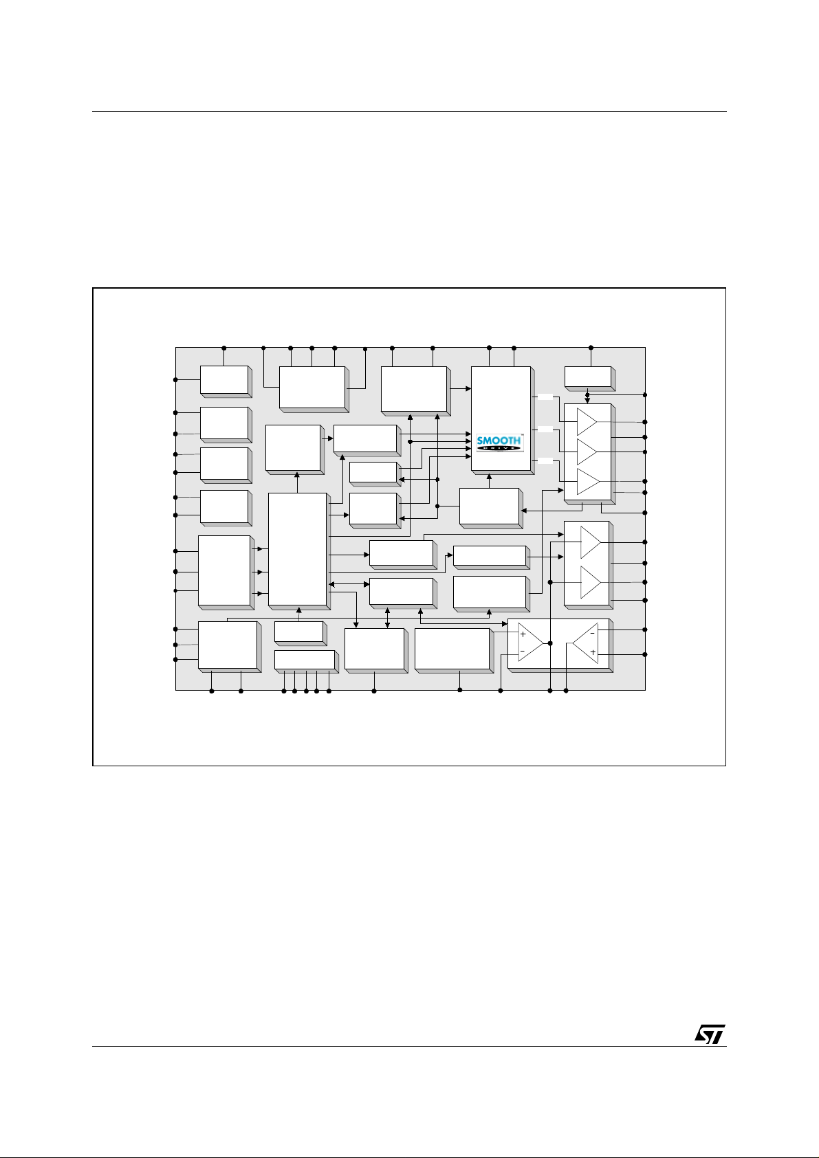
BLOCK DIAGRAM
PUMP
VREG3.3_IN
VREG2.5_IN
VREG8_DRV
VREG8_IN
SDATA
SCLK
SDEN
VBOOST
CHARGE
PUMP
3.3V
Re
ulator
2.5V
Re
ulator
8V
Re
ulator
SERIAL
PORT
SSIN
INDUCTIVE
SENSE
START-UP
REGISTERS
SSFIN
DETECTOR
SSFOUT
SHOCK
SSBUFOUT
SSOUT
BIPOLAR /
TRIPHASE
RE-SYNC
DYNAMIC/
REVERSE
BRAKE
CALIBRATION
RBIAS
FLL &
DIGITAL
FILTER
VCM
PSM/LIN
VCM
SYSCLK
RAMP LOADING
RECTIFICATION
BRAKE
SPINDLE
Architecture
BEMF
DETECTION
BEMF
FCOM
PWM A
PWM B
PWM C
VPS
ISOFET
A B
C
A+ A-
VCC
OUT_A
CTAP
OUT_B
OUT_C
RSENSE
ISENSE
VCM_A+
VCC
VCM_AVCM_GND
TR_12V
TR_5V
TR_3.3V
SUPPLY
FAULT
MONITORS
PORB
TR_2.5V
THERMAL
SUPPLY
VDD
AVCC
DGND
GND
AGND
14 BIT
VCM DAC
DAC_OUT
REFERENCE
VOLTAGE VCC/4
& GAIN SWITCH
GAINRES
A=4
ERROR_IN
ERROR_OUT
SENSE_IN-
SENSE_IN+
SENSE_OUT
2/23

SPINDLE SMOOTHDRIVE™ ARCHITECTU RE, START-UP & FLL
L7200
BIPOLAR /
TRIPHASE
SPIN-UP
INDUCTIVE
SENSE
A/D 7bit
MEMORY AND
MEMORY SCAN
TORQUE
OPTIMIZER
SERIAL PORT
6bit
8bit
FEED
FORWARD
DIGITAL
MULTIPLIER
KFLL
REGISTER
8bit
3x
9bit
10bit
10bit 12bit
d
DIGITAL
FILTER
10bit
FREQUENCY
MULTIPLIER
BYTE TO
PWM
CONVERTER
9bit
Resolution
3x
10bit2x12bit
Z.C.
PWM A
PWM B
PWM C
FLL
BEMF
DETECTION
AB
POWERS
C
PIN CONNECTION (Top view)
VCM_A+
VCM_A+
VCM_GND
VCM_GND
VCM_AVCM_A-
OUT_A
OUT_A
RSENSE
RSENSE
OUT_B
OUT_B
RSENSE
RSENSE
OUT_C
OUT_C SSFIN
SDEN
VPS
VPS
VCC
VCC
49
50
51
52
53
54
55
56
57
58
59
60
61
62
63
64
1
2 3 4 5 6 7 8 9 10 11 12 13 14 15 16
VPS
VCC
VPS
VCC
SDATA
SCLK
GND
L7200
"MOZART"
FCOM
SYSCLK
VDD
GND
DGND
BRAKE
SENSE_OUT
ERROR_OUT
ERROR_IN
CTAP
ISENSE
GAINRES
VREG8_IN
SENSE_IN-
SENSE_IN+
PUMP
SSOUT
VBOOST
33343536373839404142434445464748
DAC_OUT
32
31
PORB
30
VREG3.3_IN
VREG3.3_DRV
29
28
VREG2.5_IN
27
VREG2.5_DRV
26
RBIAS
25
AVCC
24
AGND
23
TR_12V
22
TR_5V
TR_3.3V
21
TR_2.5V
20
SSIN
19
18
SSBUFOUT
17
SSFOUT VREG8_DRV
3/23
L7200
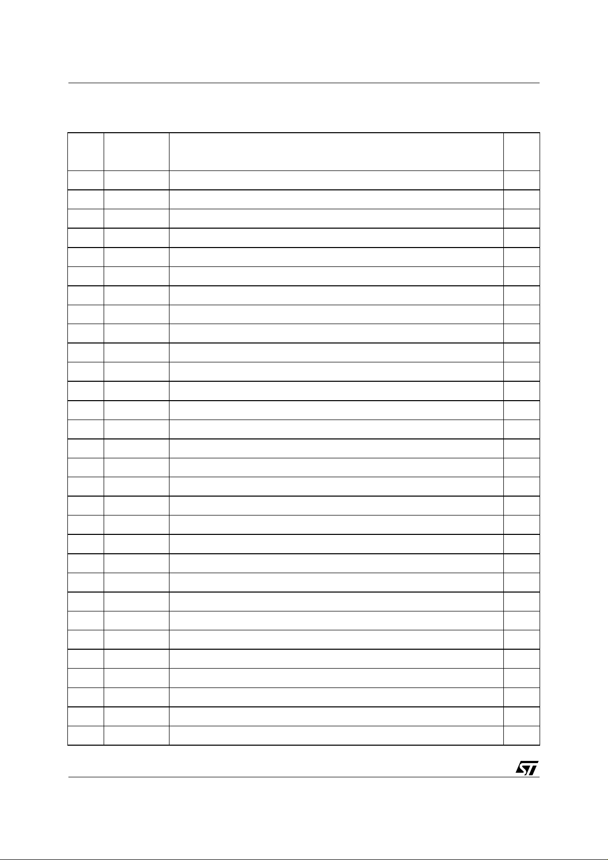
PIN FUNCTION
Pin Types: D = Digital, P = Power, A = Analog
N° Pin Name Description Type
1,2 VCC +12V Power Supply after ISOFET. P
3,4 VPS +12V Power Supply. P
5 GND Power Ground (substrate). P
6 SYSCLK Clock Frequency for system timers and counters D
7 FCOM Output of Spindle zero crossing or Current Sense circuit D
8 VD D Digital +5V Supply D
9 BRAKE Storage capacitor for brake circuit. Typically 5.9V A
10 ISENSE Input to sense the voltage of the SPINDLE Sense Resistor. A
11 CTAP Spindle Center Tap used for Differential BEMF sensing A
12 GAINRES External resistor for VCM switch gain. A
13 VBOOST External main Charge Pump Capacitor (typically VCC+5.8V) A
14 PUMP External Charge Pump A
15 SSOUT Shock Sensor detector Digital Output D
16 SSFOUT Shock Sensor detector filter Output A
17 SSFIN Shock Sensor detector filter Input A
18 SSBUFOUT Shock Sensor detector amplifier Output A
19 SSIN Shock Sensor detector amplifier Input A
20 TR_2.5V Set Point Input for 2.5V Supply monitor A
21 TR_3.3V Set Point Input for 3.3V Supply monitor A
22 TR_5V Set Point Input for 5V Supply monitor A
23 TR_12V Set Point Input for 12V Supply monitor A
24 AGND Analog Ground A
25 AVCC +12V analog Supply (after ISOFET) P
26 RBIAS External resistor for setting accurate bias current A
27 VREG2.5_DR 2.5V positive regulator drive output A
28 VREG2.5_IN 2.5V positive regulator sense input A
VREG3.3_DRV
29
30 VREG3.3_IN 3.3V positive regulator sense input A
3.3V positive regulator drive output A
31 PORB Power On Reset Output A
32 DAC_OUT Output of VCM DAC A
33 VREG8_DRV 8V positive regulator drive output A
4/23
L7200
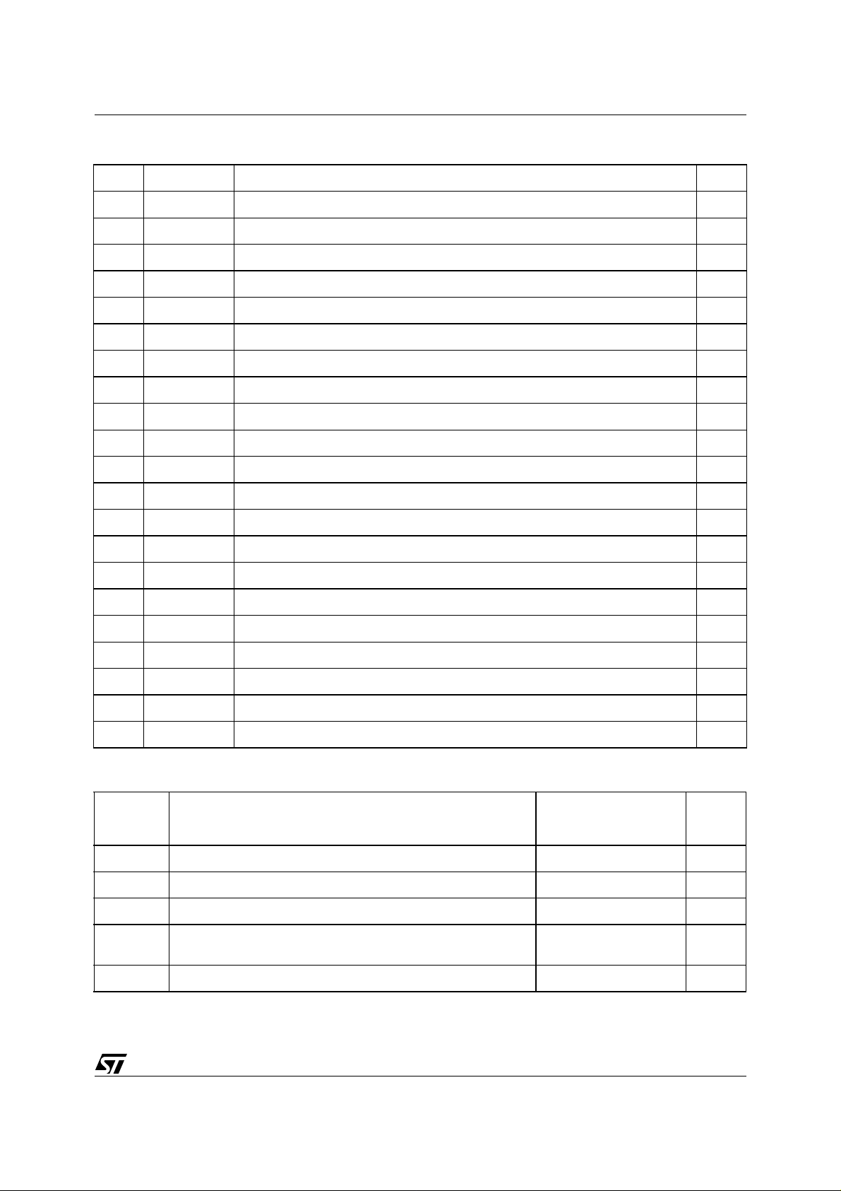
PIN FUNCTION
N° Pin Name Description Type
34 VREG8_IN 8V positive regulator sense input A
35 SENSE_IN- Inverting Input of the Sense Amplifier A
36 SENSE_IN+ Non inverting Input of the Sense Amplifier A
37 SENSE_OUT Output of the Sense Amplifier A
38 ERROR_OUT Output of the Error Amplifier A
39 ERROR_IN Inverting Input of the Error Amplifier A
40 DGND Digital Ground D
41 SDEN Serial Data Enable. Active high input pin for serial port enable D
42 SDATA Serial port Data input/output D
43 SCLK Serial Port Data Clock. Positive edge triggered clock input for serial data D
44 GND Power Ground (substrate). P
45,46 VPS +12V Power Supply. P
47,48 VCC +12V Power Supply after ISOFET. P
49,50 VCM_A+ VCM Power Amplifier positive Output terminal. A
(continued)
51,52 VCM_GND Ground for VCM power section. A
53,54 VCM_A- VCM Power Amplifier negative Output terminal. A
55,56 OUT_A Spindle DMOS half bridge Output and Input A for BEMF sensing. A
57,58 RSENSE Output Connection for the Motor Current Sense Resistor to ground. A
59,60 OUT_B Spindle DMOS half bridge Output and Input B for BEMF sensing. A
61,62 RSENSE Output Connection for the Motor Current Sense Resistor to ground. A
63,64 OUT_C Spindle DMOS half bridge Output and Input C for BEMF sensing. A
ABSOLUTE MAXIMUM RATINGS
Symbol Parameter Value Unit
Vcc Maximum Supply voltage -0.5 to 14 Volts
Vdd Maximum Logic supply -0.5 to 6 Volts
Vin max Maximum digital input voltage Vdd + .3 volts Volts
Vin min Minimum digital input voltage GND - .3 volts Volts
SPINDLE
Ipeak
VCM Ipeak VCM peak sink/source output current 1.8 Amps
Spindle peak sink/source output current 2.6 Amps
5/23
L7200
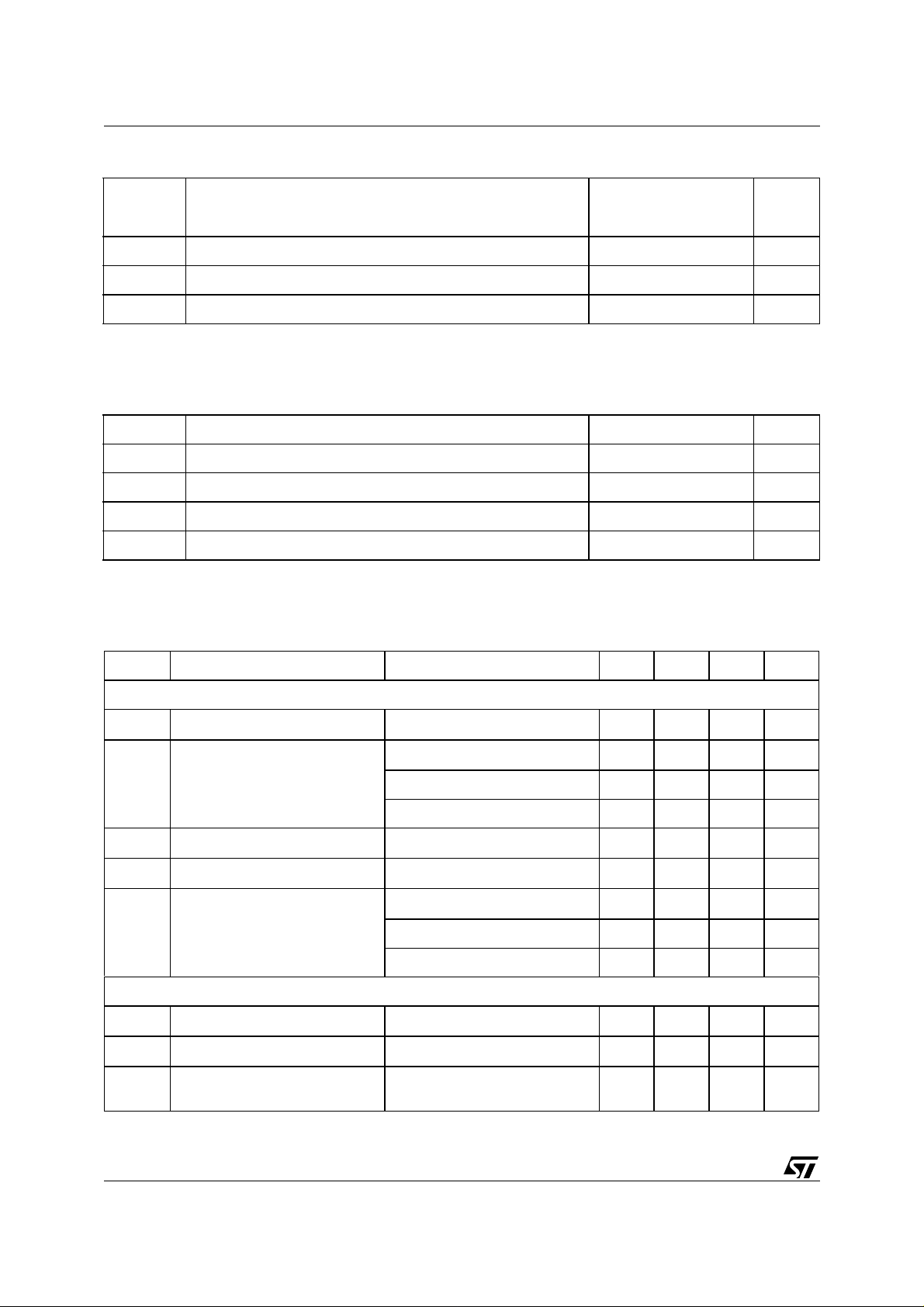
THERMAL DATA
Symbol Parameter Value Unit
θ(jc) Thermal resistance Junction to case ≈11 °C/Watt
θ(ja)* Thermal resistance Junction to ambient ≈40 °C/Watt
Ptot* Maximum Total Power Dissipation ≈2.0 Watt
Tstg,Tj Maximum storage/junction temperature -40 to 150 °C
* In typical application with multi la yer 120x120 m m Printed Circ ui t Board.
RECOMMENDED OPERATING CONDITIONS
Symbol Parameter Value Unit
Vdd Supply Voltage 10.8 to 13.2 V
Vcc Logic Supply Voltage 4.5 to 5.5 V
Tamb Operating Ambient Temperature 0 to 70 °C
Tj Junction Temperature 0 to 125 °C
ELECTRICAL CHARACTERISTCS
All specifications are for 0<Tamb<70°C, VCC=12V, VDD=5V, unless otherwise noted.
Symbol Parameter Test Condition Min. Typ. Max. Unit
POWER SUPPLIES
12V supply 10.8 13.2 V
V
CC
I
VCC
V
rectified
V
I
THERMAL SENSING
T
T
Vcc Current SPINDLE + VCM TBD mA
SPINDLE ONLY TBD mA
VCM ONLY TBD mA
Vcc supply rectified 3.5 13.2 V
5V supply 4.5 5.5 V
dd
5V supply SPINDLE + VCM TBD mA
vdd
SPINDLE ONLY TBD mA
VCM ONLY TBD mA
SHUTDOWN TEMPERATURE 150 180 °C
SD
HYSTERESIS 60 °C
HYS
6/23
T
EARLY WARNING TSD-
EW
°C
25
L7200
ELECTRICAL CHARACTERISTCS
(continued)
Symbol Parameter Test Condition Min. Typ. Max. Unit
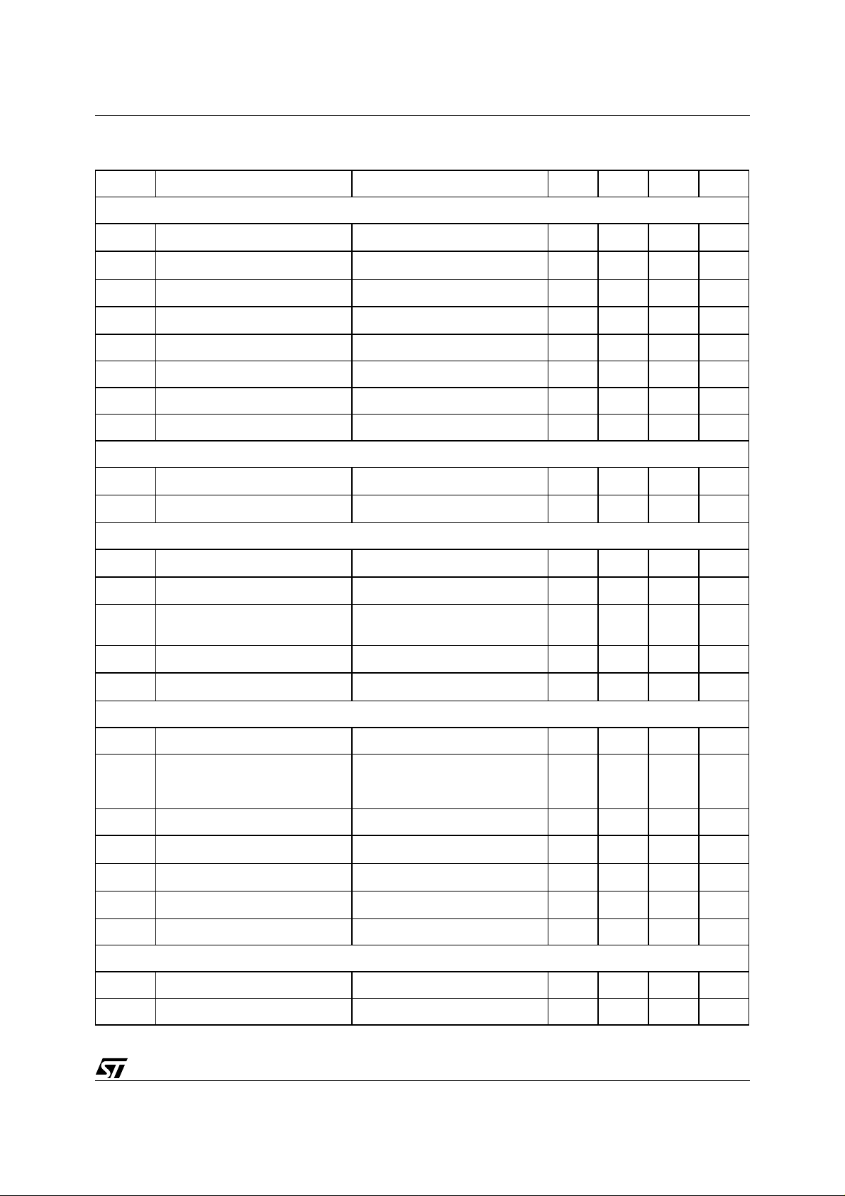
SUPPLY MONITOR
V
V
R
on_por
T
PorDly
TRIP POINT 2.5V-3.3V-5V-12V INPUT RISING 1.20 1.25 1.30 V
TR
HYSTERESIS VOLTAGE INPUT FALLING 25 mV
HYS
PORB PULL DOWN Ron Vdd > 2V and sink 1mA 500 W
POR Delay Time 80 mSec
12VTR Minimum Voltage 12V 8.6 V
5VTR Minimum Voltage 5V 4.2 V
3.3VTR Minimum Voltage 3.3V 3.135 V
2.5VTR Minimum Voltage 2.5V 2.375 V
VOLTAGE BOOST
V
BOOST
F
OUTPUT VOLTAGE VCC+5
INTERNAL OSCI LLATOR 200 KHz
OSC
VCC+6.3
SW1 OUTPUT
V
INPUT LOGIC "1" 2.4 V
IH
V
V
V
INPUT LOGIC "0" 0.5 V
IL
OUTPUT LOGIC "1" ISOURCE = 20µAVdd-
OH
V
0.2
V
F
SYSCLK
OUTPUT LOGIC "0" ISOURCE = -400µA 0.4V
OL
SYSTEM CLOCK 20 25 MHz
VCM, DAC
RESOLUTION 14 BITS
DIFFERENTIAL LINEARITY 1 LSB Change
- Tested
- By design
-1
-0.5
1
0.5
INTEGRAL LINEARITY 9 BITS
MIDSCALE OFFSET REFERENCED TO V
CONVERTION TIME 5 µs
T
C
FULL SCALE VOLTAGE REFERENCED TO V
CC/4
CC/4
-5 5 mV
±1 V
FULL SCALE ERROR -6 6 %
VCM, ERROR AMPLIFIER
AVOL OPEN LOOP GAIN DC 80 dB
LSB
VOS INPUT OFFSET VOLTAGE 1 mV
7/23
 Loading...