2A QUAD DAR LINGTON SWITC H
SUSTAINING VOLTAGE: 70 V
2 A OUTPUT
HIGH CURRENT GAIN
IDEAL FOR DRIVING SOLENOIDS, DC
MOTORS, STEPPER MOTORS, RELAYS,
DISPLAYS, ETC.
DESCRIPTION
The L702 is a monolithic integrated circuit for high
current and high voltage switching applications. It
comprises four darlingt on transist ors with commo n
emitter and open collector suitable for current s inking applications mounted on the new POWERDIP
and Multiwatt® packages.
This circuit reduces co mponents, sizes and costs;
it can provide direct interface between low level
logic and a variety of high current applications.
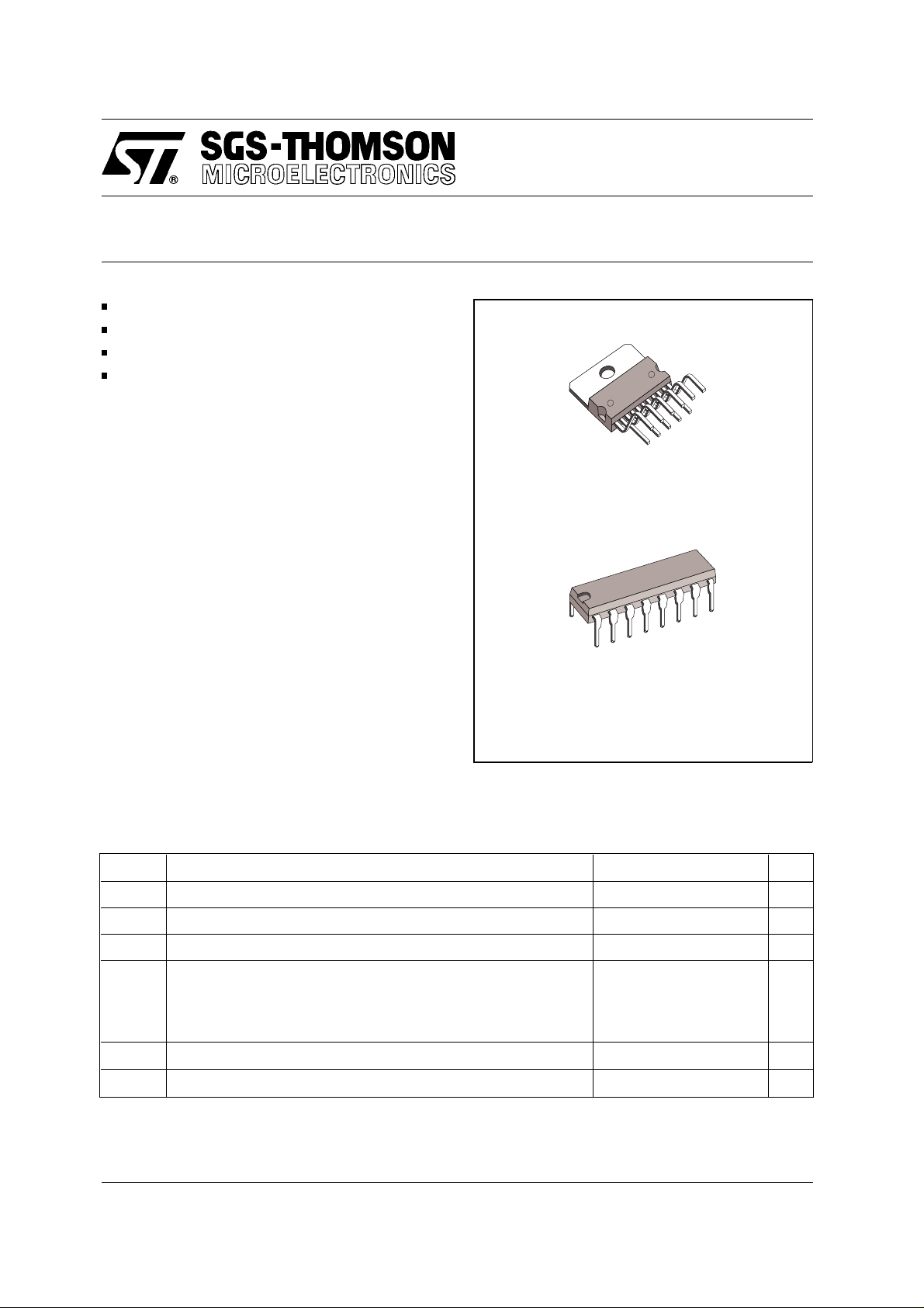
L702
Multiwatt-11
Powerdip 8 + 8
ORDER CODES : L702B - Powerdip
L702N - Multiwatt
ABSOLUTE MAXIMUM RATINGS
Symbol Parameter Value Unit
V
P
T
October 1991
Collector-emitter Voltage (input open) 90 V
CEX
V
Input Voltage 30 V
i
I
Collector Current 3 A
C
Total Power Dissipation at T
tot
Total Power Dissipation at T
Total Power Dissipationa t T
Storage Temperature -55 to 150
stg
Operating Junction Temperature -25 to 150
T
j
9 to 16 ≤ 90 °C
pin
≤ 70 °C
amb
≤ 90 °C
case
}
Powerdip
Multiwatt 20 W
4W
1.1 W
°C
°C
1/7

L702
STEPPING MOTOR BUFFER
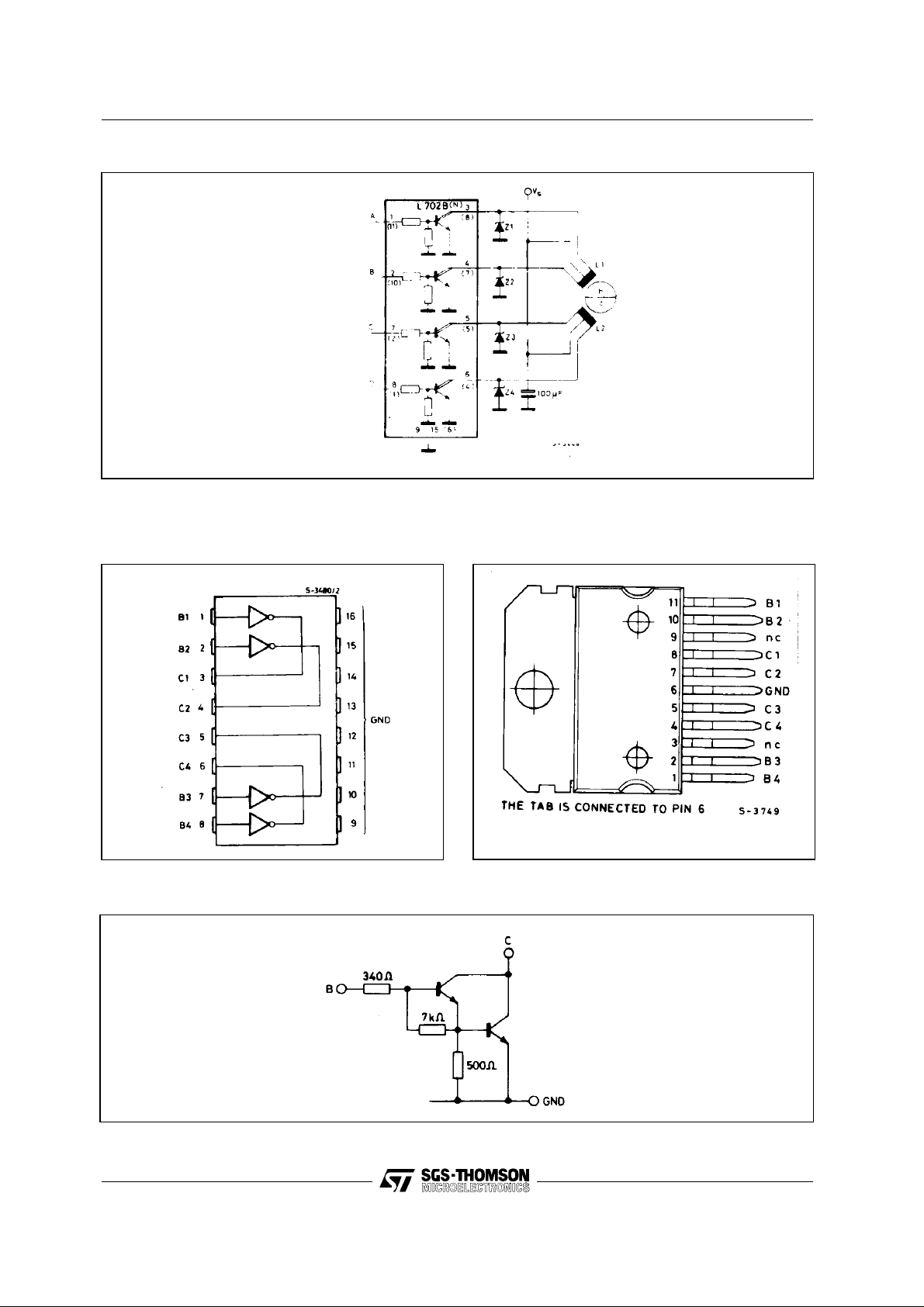
CONNECT IO N DIAG RA MS (top view)
Powerdip Multiwatt
SCHEMATIC DIAGRAM (each Darlingt on)
2/7

THERMAL DATA
Symbol Parameter Value Unit
R
th j-amb
R
th j-pins 9/16
R
th j-case
Thermal Resistance Junction Ambient
}
Powerdip
Thermal Resistance Junction Pins 9 to 16 Max 14
Thermal Resistance Junction-case Multiwatt Max 3
Max 70
L702
°C/W
°C/W
°C/W
ELECTRICAL CHARACTERISTICS (T
= 25°C unless otherwise specified)
case
Symbol Parameter Test conditions Min. Typ. Max. Unit
I
CEX
V
CE(sust)
V
CE(sat)
h
Output Leakage Current VCE = 90 V 10 50
Collector Emitter (°) Sustaining
Voltage
Collector Emitter Saturation
Voltage
DC Forward Current Gain IC = 1 A
FE
I
Input Current Vi = 3.75 V
i
= 100 mA
I
C
IC = 1.25 A
= 2 mA
I
i
= 3 V
V
CE
V
= 2.4 V
i
70
1.000 4.000
1.3 1.9 V
7
3
11
6
Open Collector
Input Voltage Off Condition VCE = 70 V
V
i
On Condition V
T
T
Turn On Time Vs = 12 V 0.3
on
Turn Off Time
off
CE
= 10 Ω
R
L
= 3 V
≤ 0.1 mA
I
C
≥ 1 A
I
C
1
0.4 V
2.4 V
µA
V
mA
mA
µs
µs
Figure 1. Switching Time. Figure 2. ton and t
Test Circuit.
off
3/7
 Loading...